3C-SiC growth on Si substrates via CVD: An introduction - Mansic
3C-SiC growth on Si substrates via CVD: An introduction - Mansic
3C-SiC growth on Si substrates via CVD: An introduction - Mansic

Create successful ePaper yourself
Turn your PDF publications into a flip-book with our unique Google optimized e-Paper software.
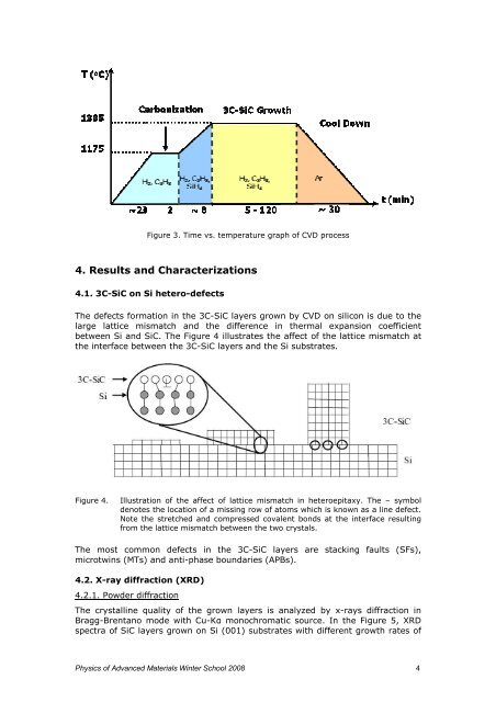
Figure 3. Time vs. temperature graph of <strong>CVD</strong> process<br />
4. Results and Characterizati<strong>on</strong>s<br />
4.1. <str<strong>on</strong>g>3C</str<strong>on</strong>g>-<str<strong>on</strong>g><strong>Si</strong>C</str<strong>on</strong>g> <strong>on</strong> <strong>Si</strong> hetero-defects<br />
The defects formati<strong>on</strong> in the <str<strong>on</strong>g>3C</str<strong>on</strong>g>-<str<strong>on</strong>g><strong>Si</strong>C</str<strong>on</strong>g> layers grown by <strong>CVD</strong> <strong>on</strong> silic<strong>on</strong> is due to the<br />
large lattice mismatch and the difference in thermal expansi<strong>on</strong> coefficient<br />
between <strong>Si</strong> and <str<strong>on</strong>g><strong>Si</strong>C</str<strong>on</strong>g>. The Figure 4 illustrates the affect of the lattice mismatch at<br />
the interface between the <str<strong>on</strong>g>3C</str<strong>on</strong>g>-<str<strong>on</strong>g><strong>Si</strong>C</str<strong>on</strong>g> layers and the <strong>Si</strong> <strong>substrates</strong>.<br />
Figure 4. Illustrati<strong>on</strong> of the affect of lattice mismatch in heteroepitaxy. The – symbol<br />
denotes the locati<strong>on</strong> of a missing row of atoms which is known as a line defect.<br />
Note the stretched and compressed covalent b<strong>on</strong>ds at the interface resulting<br />
from the lattice mismatch between the two crystals.<br />
The most comm<strong>on</strong> defects in the <str<strong>on</strong>g>3C</str<strong>on</strong>g>-<str<strong>on</strong>g><strong>Si</strong>C</str<strong>on</strong>g> layers are stacking faults (SFs),<br />
microtwins (MTs) and anti-phase boundaries (APBs).<br />
4.2. X-ray diffracti<strong>on</strong> (XRD)<br />
4.2.1. Powder diffracti<strong>on</strong><br />
The crystalline quality of the grown layers is analyzed by x-rays diffracti<strong>on</strong> in<br />
Bragg-Brentano mode with Cu-Kα m<strong>on</strong>ochromatic source. In the Figure 5, XRD<br />
spectra of <str<strong>on</strong>g><strong>Si</strong>C</str<strong>on</strong>g> layers grown <strong>on</strong> <strong>Si</strong> (001) <strong>substrates</strong> with different <str<strong>on</strong>g>growth</str<strong>on</strong>g> rates of<br />
Physics of Advanced Materials Winter School 2008 4