3C-SiC growth on Si substrates via CVD: An introduction - Mansic
3C-SiC growth on Si substrates via CVD: An introduction - Mansic
3C-SiC growth on Si substrates via CVD: An introduction - Mansic

You also want an ePaper? Increase the reach of your titles
YUMPU automatically turns print PDFs into web optimized ePapers that Google loves.
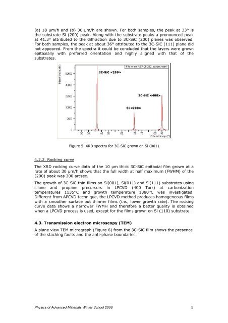
(a) 18 µm/h and (b) 30 µm/h are shown. For both samples, the peak at 33° is<br />
the substrate <strong>Si</strong> (200) peak. Al<strong>on</strong>g with the substrate peaks a pr<strong>on</strong>ounced peak<br />
at 41.3° attributed to the diffracti<strong>on</strong> due to <str<strong>on</strong>g>3C</str<strong>on</strong>g>-<str<strong>on</strong>g><strong>Si</strong>C</str<strong>on</strong>g> (200) planes was observed.<br />
For both samples, the peak at about 36° attributed to the <str<strong>on</strong>g>3C</str<strong>on</strong>g>-<str<strong>on</strong>g><strong>Si</strong>C</str<strong>on</strong>g> (111) plane did<br />
not appeared. From the spectra it could be c<strong>on</strong>cluded that the layers were grown<br />
epitaxially with preferred orientati<strong>on</strong> and highly aligned with that of the<br />
<strong>substrates</strong>.<br />
4.2.2. Rocking curve<br />
Figure 5. XRD spectra for <str<strong>on</strong>g>3C</str<strong>on</strong>g>-<str<strong>on</strong>g><strong>Si</strong>C</str<strong>on</strong>g> grown <strong>on</strong> <strong>Si</strong> (001)<br />
The XRD rocking curve data of the 10 µm thick <str<strong>on</strong>g>3C</str<strong>on</strong>g>-<str<strong>on</strong>g><strong>Si</strong>C</str<strong>on</strong>g> epitaxial film grown at a<br />
rate of about 30 µm/h shows that the full width at half maximum (FWHM) of the<br />
(200) peak was 300 arcsec.<br />
The <str<strong>on</strong>g>growth</str<strong>on</strong>g> of <str<strong>on</strong>g>3C</str<strong>on</strong>g>-<str<strong>on</strong>g><strong>Si</strong>C</str<strong>on</strong>g> thin films <strong>on</strong> <strong>Si</strong>(001), <strong>Si</strong>(011) and <strong>Si</strong>(111) <strong>substrates</strong> using<br />
silane and propane precursors in LP<strong>CVD</strong> (400 Torr) at carb<strong>on</strong>izati<strong>on</strong><br />
temperatures 1135°C and <str<strong>on</strong>g>growth</str<strong>on</strong>g> temperature 1380°C was investigated.<br />
Different from AP<strong>CVD</strong> technique, the LP<strong>CVD</strong> method produces homogeneous films<br />
with a smoother surface but thinner films (i.e., lower <str<strong>on</strong>g>growth</str<strong>on</strong>g> rate). The rocking<br />
curve data shows a narrower FWMH and therefore a better quality is obtained<br />
when a LP<strong>CVD</strong> process is used, except for the films grown <strong>on</strong> <strong>Si</strong> (110) substrate.<br />
4.3. Transmissi<strong>on</strong> electr<strong>on</strong> microscopy (TEM)<br />
A plane view TEM micrograph (Figure 6) from the <str<strong>on</strong>g>3C</str<strong>on</strong>g>-<str<strong>on</strong>g><strong>Si</strong>C</str<strong>on</strong>g> film shows the presence<br />
of the stacking faults and the anti-phase boundaries.<br />
Physics of Advanced Materials Winter School 2008 5