3C-SiC growth on Si substrates via CVD: An introduction - Mansic
3C-SiC growth on Si substrates via CVD: An introduction - Mansic
3C-SiC growth on Si substrates via CVD: An introduction - Mansic

Create successful ePaper yourself
Turn your PDF publications into a flip-book with our unique Google optimized e-Paper software.
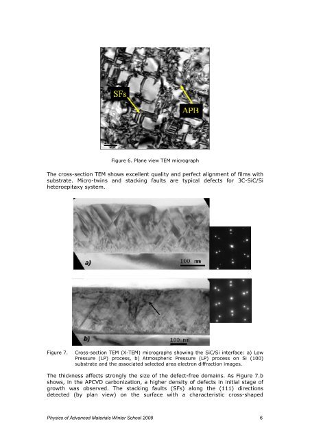
Figure 6. Plane view TEM micrograph<br />
The cross-secti<strong>on</strong> TEM shows excellent quality and perfect alignment of films with<br />
substrate. Micro-twins and stacking faults are typical defects for <str<strong>on</strong>g>3C</str<strong>on</strong>g>-<str<strong>on</strong>g><strong>Si</strong>C</str<strong>on</strong>g>/<strong>Si</strong><br />
heteroepitaxy system.<br />
Figure 7. Cross-secti<strong>on</strong> TEM (X-TEM) micrographs showing the <str<strong>on</strong>g><strong>Si</strong>C</str<strong>on</strong>g>/<strong>Si</strong> interface: a) Low<br />
Pressure (LP) process, b) Atmospheric Pressure (LP) process <strong>on</strong> <strong>Si</strong> (100)<br />
substrate and the associated selected area electr<strong>on</strong> diffracti<strong>on</strong> images.<br />
The thickness affects str<strong>on</strong>gly the size of the defect-free domains. As Figure 7.b<br />
shows, in the AP<strong>CVD</strong> carb<strong>on</strong>izati<strong>on</strong>, a higher density of defects in initial stage of<br />
<str<strong>on</strong>g>growth</str<strong>on</strong>g> was observed. The stacking faults (SFs) al<strong>on</strong>g the (111) directi<strong>on</strong>s<br />
detected (by plan view) <strong>on</strong> the surface with a characteristic cross-shaped<br />
Physics of Advanced Materials Winter School 2008 6