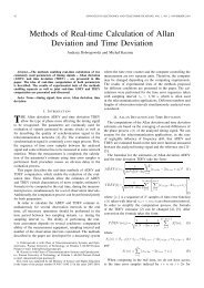
november 2010 volume 1 number 2 - Advances in Electronics and ...
november 2010 volume 1 number 2 - Advances in Electronics and ...
november 2010 volume 1 number 2 - Advances in Electronics and ...

Create successful ePaper yourself
Turn your PDF publications into a flip-book with our unique Google optimized e-Paper software.
50 ADVANCES IN ELECTRONICS AND TELECOMMUNICATIONS, VOL. 1, NO. 2, NOVEMBER <strong>2010</strong><br />
Fig. 4. Vernier block diagram.<br />
They depend exclusively on supply voltage <strong>and</strong> temperature.<br />
Simultaneous control over the period length <strong>and</strong> frequency is<br />
realized by the last factor.<br />
The rema<strong>in</strong><strong>in</strong>g part of the system is a technical realization<br />
of expression (7). It is presented <strong>in</strong> a block diagram <strong>in</strong> Fig. 5.<br />
Theexam<strong>in</strong>edmeasurementsignalissentatthe<strong>in</strong>putcircuit<br />
which generated signals START <strong>and</strong> STOP at its <strong>in</strong>put. The<br />
time unit between these signals is directly proportional to the<br />
exam<strong>in</strong>ed <strong>in</strong>terval.<br />
From equation (10) we can calculate that the shortest<br />
possible period that can be achieved is ca 18,5 ns, which<br />
gives a frequency approximately equal to 54 MHz. When<br />
the co<strong>in</strong>cidence of pulses from both generators appears, the<br />
detection system generates a co<strong>in</strong>cidence signal ST stopp<strong>in</strong>g<br />
the work of both generators. Dur<strong>in</strong>g the whole operation the<br />
systems of counters count pulses from both generators n1 <strong>and</strong><br />
n2. After read<strong>in</strong>g, a microprocessor makes the calculations of<br />
the exam<strong>in</strong>ed <strong>in</strong>terval ∆t, resets the counters, <strong>and</strong> then grants<br />
another measurement. The measurement result is displayed on<br />
the monitor of a computer cooperat<strong>in</strong>g with the microprocessor.<br />
Thanks to the application of two generators which conta<strong>in</strong><br />
<strong>in</strong>dependentdelay systemsDS1020-15,it ispossible to choose<br />
an appropriate value of τ, dependent only on the difference<br />
of words programm<strong>in</strong>g the delay systems. Assum<strong>in</strong>g a too<br />
small difference, e.g. 50 ps, causes an <strong>in</strong>stability of generators<br />
because the <strong>in</strong>stability comprises that difference.<br />
Assum<strong>in</strong>g a too big value of τ places the application of<br />
this methodunderthe questionmark becausethe improvement<br />
of resolution is very slight. In the manufactured model the<br />
value of τ 200 ps was assumed, which is an equivalent to the<br />
frequency of reference generator with value 5 GHz.<br />
V. SUMMARY<br />
The develop<strong>in</strong>g of the vernier circuit enabled the estimation<br />
of its performance. The fundamental objective has<br />
been achieved, i.e. the test<strong>in</strong>g of the vernier method <strong>and</strong> its<br />
optimization <strong>in</strong> the frame of the technology applied. The tests<br />
have answered the follow<strong>in</strong>g questions: which elements of the<br />
slotted l<strong>in</strong>e are responsible for process<strong>in</strong>g errors, <strong>and</strong> which<br />
po<strong>in</strong>ts of the system corrections should be <strong>in</strong>troduced. The<br />
ma<strong>in</strong> task at present is to reduce the manufactured device<br />
to FPGA technology, which will elim<strong>in</strong>ate the trouble of<br />
generators of the vernier itself <strong>and</strong> improve their parameters;<br />
a decrease <strong>in</strong> resolution is especially desired. The purpose of<br />
further effort is to achieve a resolution level of 20 ps.<br />
REFERENCES<br />
[1] S. Bregni, Synchronization of Digital Telecommunications Networks. J.<br />
Wiley&Sons, 2002.<br />
[2] [onl<strong>in</strong>e], pl.wikipedia.org/wiki/Noniusz.<br />
[3] J. Kalisz, R. Pe´lka, <strong>and</strong> R. Szplet, “Design problems <strong>in</strong> precise metrology<br />
of time units,” <strong>in</strong> Proc.of MWK conference, Rynia, 2001, pp. 117–165.<br />
[4] J. J˛erzejewski, “The application of the idea vernier to precise measurement<br />
of time <strong>in</strong>terval,” Master’s thesis, Poznan University of Technology,<br />
2008, supervisor Krzysztof Lange.<br />
[5] Catalog note of Dallas company.<br />
Krzysztof Lange was born <strong>in</strong> Poznan, Pol<strong>and</strong>, <strong>in</strong> 1945. He received his<br />
M.Sc. degree <strong>in</strong> 1969 <strong>and</strong> Ph.D. degree <strong>in</strong> 1978 from Poznan University<br />
of Technology. His research concentrates on synchronization <strong>in</strong> telecommunication<br />
networks <strong>and</strong> systems, digital circuit application <strong>and</strong> time <strong>and</strong><br />
frequency metrology. He is currently an Assistant Professor at the Chair of<br />
Telecommunication Systems <strong>and</strong> Optoelectronics, PUT<br />
Michal Kasznia was born <strong>in</strong> Poznan, Pol<strong>and</strong>, <strong>in</strong> 1971. He received his<br />
M.Sc. degree <strong>in</strong> electronics <strong>and</strong> telecommunications <strong>in</strong> 1994 <strong>and</strong> Ph.D. degree<br />
<strong>in</strong> telecommunications <strong>in</strong> 2002 from Poznan University of Technology. His<br />
research concentrates on synchronization <strong>in</strong> telecommunication networks <strong>and</strong><br />
systems, especially on tim<strong>in</strong>g <strong>and</strong> carrier recovery us<strong>in</strong>g DSP technology, <strong>and</strong><br />
analysis of the quality of synchronization signals. He is currently an Assistant<br />
Professor at the Chair of Telecommunication Systems <strong>and</strong> Optoelectronics,<br />
PUT