november 2010 volume 1 number 2 - Advances in Electronics and ...
november 2010 volume 1 number 2 - Advances in Electronics and ...
november 2010 volume 1 number 2 - Advances in Electronics and ...

You also want an ePaper? Increase the reach of your titles
YUMPU automatically turns print PDFs into web optimized ePapers that Google loves.
70 ADVANCES IN ELECTRONICS AND TELECOMMUNICATIONS, VOL. 1, NO. 2, NOVEMBER <strong>2010</strong><br />
Bit Error Rate Tester for 10 Gb/s Fibre Optic L<strong>in</strong>k<br />
Łukasz ´Sliwczyński <strong>and</strong> Przemysław Krehlik<br />
Abstract—The bit error rate tester suitable for operation<br />
<strong>in</strong> 10 Gb/s fibre optic l<strong>in</strong>ks is described <strong>in</strong> the paper. The<br />
BER tester was built from commercially available components.<br />
Generation <strong>and</strong> reception of 10 Gb/s data stream is performed<br />
with help of high-speed serialiser <strong>and</strong> deserialiser by Maxim. The<br />
ma<strong>in</strong> functions of the BER tester are implemented <strong>in</strong> the field<br />
programmable gate array (FPGA) Spartan3 device by Xil<strong>in</strong>x.<br />
The part of the FPGA runs with the clock speed equal to 622<br />
MHz. Some measurement results obta<strong>in</strong>ed <strong>in</strong> the fibre optic l<strong>in</strong>ks<br />
operated with 10 Gb/ data rate are also presented.<br />
Index Terms—bit error rate, fibre optic l<strong>in</strong>ks, field programmable<br />
gate arrays<br />
I. INTRODUCTION<br />
BIT error rate (BER) is one of the most important parameters<br />
describ<strong>in</strong>g the performance of transmission <strong>in</strong> the<br />
digital l<strong>in</strong>k. It is usually def<strong>in</strong>ed as:<br />
BER = ne<br />
, (1)<br />
N<br />
where ne is the total <strong>number</strong> of received bits <strong>and</strong> N is the<br />
<strong>number</strong> of bits be<strong>in</strong>g <strong>in</strong> error. Because of r<strong>and</strong>om nature of<br />
the phenomenon, BER is also regarded as the probability of<br />
errors occurr<strong>in</strong>gdur<strong>in</strong>g data transmission. BER <strong>in</strong> the order of<br />
10 −9 or even 10 −12 is often considered as be<strong>in</strong>g characteristic<br />
for modern fibre optic systems. Because of that, measur<strong>in</strong>g<br />
BER accord<strong>in</strong>gly to equation (1) is <strong>in</strong>convenient as it would<br />
require us<strong>in</strong>g a counter with huge capacity (generally, greater<br />
than 1/BER. Thus, it is better to transform equation (1) <strong>in</strong>to:<br />
BER = 1 ne<br />
, (2)<br />
B ∆t<br />
where B is the bit rate <strong>and</strong> ∆t is the measurementtime. When<br />
us<strong>in</strong>g equation (2), it is convenient to express ∆t <strong>in</strong> seconds,<br />
<strong>and</strong> the bit rate is only a scal<strong>in</strong>g factor.<br />
Nowadays 10 Gb/s transmission rate is <strong>in</strong>creas<strong>in</strong>gly common<br />
<strong>in</strong> fibre optic l<strong>in</strong>ks. Commercial BER testers capable<br />
of operation with such fast signals are often very advanced<br />
(e.g. [1]–[3]). They allow the test<strong>in</strong>g of a transmission system<br />
more comprehensively (for example to check its immunity to<br />
jitter or pathological data patterns), not just to simply measure<br />
BER. Unfortunately, the cost of such test systems is very<br />
high, which make them rarely available for most universities<br />
research/students labs. Thus, an idea was born to develop 10<br />
Gb/s BER tester (BERT), which would be possible to be built<br />
from commercially available components, with most of its<br />
functions be<strong>in</strong>g implemented <strong>in</strong> the FPGA circuit. Below a<br />
Łukasz ´Sliwczyński is with the AGHUniversity ofScience <strong>and</strong> Technology,<br />
Mickiewicza 30 Ave., 30-059 Krakow, Pol<strong>and</strong> (phone: +48 12-617-27-40, fax:<br />
+48-12-633-23-98, e-mail: sliwczyn@agh.edu.pl)<br />
Przemysław Krehlik iswiththeAGHUniversity ofScience <strong>and</strong> Technology,<br />
Mickiewicza 30 Ave., 30-059 Krakow, Pol<strong>and</strong> (e-mail: krehlik@agh.edu.pl)<br />
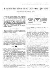
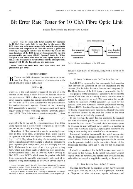
Fig. 1. Generic block diagram of the BER tester.<br />
design of such BERT is presented, along with a theory of its<br />
operation.<br />
II. IDEA OF OPERATION OF THE BER TESTER<br />
Each BERT is composed of two ma<strong>in</strong> parts: the transmitter<br />
(that <strong>in</strong>cludes the generator of the test sequences) <strong>and</strong> the<br />
receiver (that <strong>in</strong>cludes the error detector <strong>and</strong> analyser) [4].<br />
The block diagram of the BER tester is presented <strong>in</strong> Fig. 1.<br />
The purposeof the test sequence generatoris to producethe<br />
stream of the data bits accord<strong>in</strong>g to some rule that must be<br />
known for the receiver as well. The most often the pseudo<br />
r<strong>and</strong>om bit sequence (PRBS) generators are used for this<br />
purpose. There are a <strong>number</strong> of st<strong>and</strong>ard polynomialsdef<strong>in</strong><strong>in</strong>g<br />
different PRBS, developed by st<strong>and</strong>ardisation bodies (e.g. [5])<br />
for test<strong>in</strong>g telecommunication equipment. Alternatively, some<br />
bit sequence def<strong>in</strong>ed by the user <strong>and</strong> stored <strong>in</strong> the tester<br />
memory may be periodically generated.<br />
In the receiver, the error detector compares the received<br />
bits with the orig<strong>in</strong>al pattern <strong>and</strong>, <strong>in</strong> case of <strong>in</strong>compatibility,<br />
<strong>in</strong>creasesthe errorcounter.Theresult ofthemeasurementmay<br />
be presented <strong>in</strong> many different ways: simply as a <strong>number</strong>, or<br />
<strong>in</strong> the form of detailed diagram, display<strong>in</strong>g the <strong>number</strong> of bits<br />
be<strong>in</strong>g <strong>in</strong> error dur<strong>in</strong>g each second of the measurement.<br />
Because of the delay <strong>in</strong>troduced by the tested transmission<br />
l<strong>in</strong>k, the measurement process must be preceded by the synchronisationofthelocaltest<br />
sequencegenerator<strong>in</strong>thereceiver<br />
with the generator <strong>in</strong>cluded <strong>in</strong> the transmitter. Details of this<br />
process are described <strong>in</strong> [4] <strong>and</strong> [6] <strong>and</strong> will not be discussed<br />
here.<br />
It should be mentioned that the BER measurement must be<br />
performed on the formed, digital signal with clearly def<strong>in</strong>ed<br />
logical levels. In particular, the transmission clock is required<br />
to be either recovered or supplied externally to the receiver.<br />
III. BER TESTER FOR 10 GB/S SYSTEM<br />
The idea described <strong>in</strong> the previous section may be applied<br />
to the signal with any bit rate, at least <strong>in</strong> pr<strong>in</strong>ciple. However,<br />
at Gb-per-second data rates some special techniques <strong>and</strong>