Science Opportunities in Azerbaijan - Science and Technology ...
Science Opportunities in Azerbaijan - Science and Technology ...
Science Opportunities in Azerbaijan - Science and Technology ...

Create successful ePaper yourself
Turn your PDF publications into a flip-book with our unique Google optimized e-Paper software.
<strong>Technology</strong> Profile<br />
Obta<strong>in</strong><strong>in</strong>g of the Charged Nanoparticles by<br />
Means of the Po<strong>in</strong>t Ion Source<br />
Description<br />
The means of disperse phase of the po<strong>in</strong>t ion source have<br />
been used for obta<strong>in</strong><strong>in</strong>g of the charged nanoparticles. The<br />
source represents the compact graphite conta<strong>in</strong>er with the<br />
work<strong>in</strong>g matter <strong>in</strong>side of which a th<strong>in</strong> high-melt<strong>in</strong>g po<strong>in</strong>t is<br />
bulged out. The smelt matter wets a surface of po<strong>in</strong>t. Sizes<br />
of generated nanodroplets determ<strong>in</strong>ed by means of electron<br />
<strong>and</strong> AFM microscopes compose cont<strong>in</strong>uous spectrum<br />
from 2 nm up to 20 nm. The number of particles of least<br />
size on three orders of magnitude exceeds number of particles<br />
of the greatest size. The In, Sn, NiAlB have been<br />
used as work<strong>in</strong>g matters at carry<strong>in</strong>g out of our experiments.<br />
It is possible the creation of various surface quantum structures<br />
by means of these nanoparticles. Energy of the<br />
charged nanoparticles can be regulated by means of an<br />
electric field. Nanoparticles of <strong>in</strong>tr<strong>in</strong>sic semiconductors <strong>and</strong><br />
their compounds can be obta<strong>in</strong>ed <strong>in</strong> the modified design of<br />
a source with a porous po<strong>in</strong>t.<br />
Innovative Aspects <strong>and</strong> Ma<strong>in</strong> Advantages<br />
Nanoparticles are obta<strong>in</strong>ed <strong>in</strong> a ready k<strong>in</strong>d; it is not necessary<br />
to spend a long time to form them; speeds <strong>and</strong> trajectories<br />
of particles are manageable; it is possible the<br />
separation of particles <strong>in</strong> the sizes by means of the massanalyzer.<br />
It is also possible an arrangement of nanoparticles<br />
on required coord<strong>in</strong>ates of the substrate’s surface by<br />
means of probe manipulator after their deposition.<br />
Areas of Application<br />
Nanotechnology, ion-plasma technology, th<strong>in</strong>-film electronics.<br />
Stage of Development<br />
Laboratory tested technology of obta<strong>in</strong><strong>in</strong>g of the ions <strong>and</strong><br />
nanoparticles of semiconductor materials.<br />
Contact Details<br />
Institute of Physics<br />
Contact person: Hasanov Ilkham Soltan oglu<br />
Address: 33, H. Javid Avenue<br />
AZ1143, Baku, <strong>Azerbaijan</strong><br />
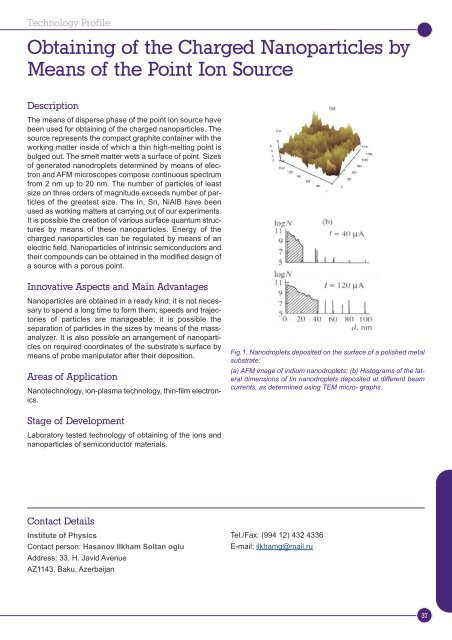
Fig.1. Nanodroplets deposited on the surface of a polished metal<br />
substrate:<br />
(a) AFM image of <strong>in</strong>dium nanodroplets; (b) Histograms of the lateral<br />
dimensions of t<strong>in</strong> nanodroplets deposited at different beam<br />
currents, as determ<strong>in</strong>ed us<strong>in</strong>g TEM micro- graphs.<br />
Tel./Fax: (994 12) 432 4336<br />
E-mail: ilkhamg@mail.ru<br />
37