Science Opportunities in Azerbaijan - Science and Technology ...
Science Opportunities in Azerbaijan - Science and Technology ...
Science Opportunities in Azerbaijan - Science and Technology ...

You also want an ePaper? Increase the reach of your titles
YUMPU automatically turns print PDFs into web optimized ePapers that Google loves.
<strong>Technology</strong> Profile<br />
New Anti – Stokes Lum<strong>in</strong>ophors <strong>and</strong> Laser Mediums<br />
on the Base of II-III 2 - VI 4 Typed Wide-B<strong>and</strong> Chalcogenide<br />
Semiconductors Doped by Rare-Earth Elements<br />
Description<br />
Traditional <strong>in</strong>vestigations, synthesis <strong>and</strong> use of anti –<br />
Stokes lum<strong>in</strong>ophors (ASL) have an objective to visualize<br />
IR-radiation, i.e. IR-signal conversion <strong>in</strong>to visible b<strong>and</strong><br />
(0.38÷0.76mkm). Recently there have been created systems<br />
of length fiber optic communication l<strong>in</strong>es where data<br />
carrier is the radiation with wavelength about 1.55 mkm.<br />
There have been developed lasers on the base of erbium<br />
glasses with wavelength of generation 1.54÷1.65 mkm.<br />
Therefore activation of wide-b<strong>and</strong> semiconductive compounds<br />
EuGa 2S 4 <strong>and</strong> YbGa 2S 4 by 4f-elements, study of impurity<br />
state <strong>and</strong> behavior is one of the central issues of<br />
physics <strong>and</strong> material science of semiconductors as a<br />
whole.<br />
Nowadays complex rare – earth compounds of MIM II<br />
2 X4VI (MI -Eu, Yl,Sm; MII-Ga,In; X VI<br />
4 - S,Se) – typed take a special<br />
place among wide - b<strong>and</strong> semiconductors.<br />
MIM II<br />
2 X4VI - typed crystals have been crystallized <strong>in</strong> rhombic<br />
s<strong>in</strong>gony, they are high – resistance (105 ÷10IIOhm/cm), wide-b<strong>and</strong> (~4.4eV) semiconductors <strong>and</strong> show particularly<br />
pronounced lum<strong>in</strong>escent <strong>and</strong> photoconductive properties.<br />
In accord<strong>in</strong>g with above- mentioned it is of <strong>in</strong>terest spectroscopic<br />
<strong>in</strong>vestigation of 4f-elements <strong>in</strong> Eu (Yb) Ga2S4 crystals.<br />
There has been developed technology of II-III2 - IV2 (II-Eu,<br />
Yb,Sm,Ca, Sr,Ba; III-Ga,Al;VI-S,Se,O) - typed semiconductors<br />
activated by rare-earth ions.<br />
Innovative Aspects <strong>and</strong> Ma<strong>in</strong> Advantages<br />
Production of effective devices for visualization <strong>and</strong> illum<strong>in</strong>ation,<br />
be<strong>in</strong>g able to compete with traditional systems requires<br />
to manufacture lum<strong>in</strong>ophors with specific properties.<br />
This necessity promotes development of new materials <strong>and</strong><br />
optimization of exist<strong>in</strong>g lum<strong>in</strong>ophors. İn this aspect perspective<br />
ones are ternary alkali-earth chalcogenide semiconductors<br />
of II-III 2 - IV 2 (II-Eu, Yb,Sm,Ca, Sr,Ba;<br />
III-Ga,Al;VI-S,Se,O) – typed activated by rare-earth ions.<br />
One of the qualities of ternary compounds compar<strong>in</strong>g<br />
favourably with b<strong>in</strong>ary one as regards applied use is the resistance<br />
to hydrolysis <strong>and</strong> good implantation of rare-earth<br />
ions <strong>in</strong>to crystal lattice. High l<strong>in</strong>earity of cathode lum<strong>in</strong>escence<br />
at high densities of current makes them suitable for<br />
use as a lum<strong>in</strong>ophor <strong>in</strong> TV <strong>and</strong> field ionization displays. Se-<br />
Contact Details<br />
Institute of Physics<br />
Contact person: Tagiev Oktay Bahadur<br />
Address: 33, H. Javid Avenue<br />
AZ1143, Baku, <strong>Azerbaijan</strong><br />
lection of correspond<strong>in</strong>g sensitizers <strong>and</strong> activators one can<br />
change efficiency of conversion of various k<strong>in</strong>ds of energy<br />
<strong>in</strong>to light one <strong>and</strong> lum<strong>in</strong>escence colors of these compounds.<br />
Areas of Application<br />
Systems of fiber optic communication l<strong>in</strong>es, lasers with<br />
wavelength of generation 1.54-1/65mkm, night vision<br />
equipments.<br />
Stage of Development<br />
Development phase - laboratory tested.<br />
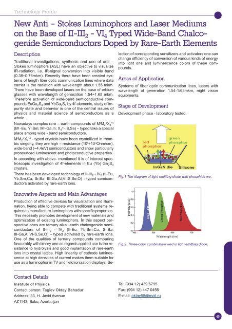
Fig.1 The diagram of light emitt<strong>in</strong>g diode with phosphide we.<br />
Fig.2. Three-color comb<strong>in</strong>ation wed <strong>in</strong> light emitt<strong>in</strong>g diode.<br />
Tel: (994 12) 439 6795<br />
Fax: (994 12) 447 0456<br />
E-mail: oktay58@mail.ru<br />
45