ΚΕΦΑΛΑΙΟ 3ΟΚΑΤΑΣΚΕΥΗ ΚΑΙ ΛΕΙΤΟΥΡΓΙΑ ΑΙΣΘΗΤΗΡΑ
ΚΕΦΑΛΑΙΟ 3ΟΚΑΤΑΣΚΕΥΗ ΚΑΙ ΛΕΙΤΟΥΡΓΙΑ ΑΙΣΘΗΤΗΡΑ
ΚΕΦΑΛΑΙΟ 3ΟΚΑΤΑΣΚΕΥΗ ΚΑΙ ΛΕΙΤΟΥΡΓΙΑ ΑΙΣΘΗΤΗΡΑ

You also want an ePaper? Increase the reach of your titles
YUMPU automatically turns print PDFs into web optimized ePapers that Google loves.
Abstract<br />
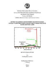
Strain sensors have been fabricated by depositing platinum nanoparticles between<br />
interdigitated gold electrodes on oxidised silicon substrate. A significant improvement in<br />
strain sensitivity is achieved with a gauge factor in excess of 700, which is two orders of<br />
magnitude higher than continuous metallic films and five times higher than semiconductor<br />
devices. The measured resistance is strongly dependent on inter-particle distance, which is<br />
altered when the substrate is strained.<br />
Traditionally strain sensors have been fabricated using either metallic strain gauges or<br />
semiconductors. The basic principle of operation of these devices is based on the change of<br />
the resistance with strain. More recently nanotechnology objects like carbon nanotubes<br />
dispensed within a polymer matrix[2, 3] have been investigated towards higher sensitivity and<br />
lower cost device. The resistance change in that case is due to intrinsic material properties of<br />
carbon nanotubes that present a high piezoresistance coefficient. It has been also<br />
demonstrated that metallic nanoparticle assemblies positioned between two conductive<br />
electrodes exhibit much higher strain sensitivity than continuous metallic films (gauge factor<br />
2) and of similar value with their semiconducting rivals (gauge factor 100). The high<br />
resistance sensitivity with strain in that case is not due to a material intrinsic property like<br />
piezoresistance but to the dominating current transport mechanism itself which is based on<br />
current tunneling through nanogaps present between nanoparticles. In the current work we<br />
investigate this type of strain sensor.<br />
We have developed during recent years, techniques for room temperature nanoparticle<br />
deposition which are based either on ink-jet printing or in vacuum[4, 5]. While ink-jet<br />
technique is simpler it presents problems related with uniformity (controlled deposition<br />
density) of nanoparticles within the deposited layer. On the other hand formation of<br />
nanoparticles in vacuum based on sputtering and condensation of atoms from a metallic target<br />
to form clusters of controlled size that are uniformly deposited on the substrate presents<br />
another alternative for uniform nanoparticle layer formation with controlled surface density.<br />
This technique that is explored in the present work presents the advantage of a better<br />
resistance control and allows optimization of the sensor operation both in terms of power<br />
dissipation and strain sensitivity.<br />
7