- Seite 2 und 3: Applikationshandbuch Leistungshalbl
- Seite 4 und 5: Vorwort Seit dem Erscheinen des ers
- Seite 6 und 7: Inhalt 1 Betriebsweise von Leistung
- Seite 8 und 9: 3.3.1 Grenzwerte ..................
- Seite 10 und 11: 5.2.3.4 Bauelementauswahl .........
- Seite 12 und 13: 1 Betriebsweise von Leistungshalble
- Seite 14 und 15: 1 Betriebsweise von Leistungshalble
- Seite 16 und 17: 1.2 Leistungselektronische Schalter
- Seite 18 und 19: 1 Betriebsweise von Leistungshalble
- Seite 20 und 21: 1 Betriebsweise von Leistungshalble
- Seite 22 und 23: AUS hart weich L K in Reihe 1 Betri
- Seite 24 und 25: 2 Grundlagen 2 Grundlagen 2.1 Einsa
- Seite 26 und 27: 2 Grundlagen Wichtige Ziele der Wei
- Seite 28 und 29: 2 Grundlagen vor allem in optoelekt
- Seite 30 und 31: Glass passivation Anode (metallized
- Seite 32 und 33: I F 0.1 I F v V FRM VF 0.1 FV F t f
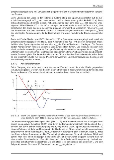
- Seite 34 und 35: 2 Grundlagen Rückwärtsstrom Der
- Seite 36 und 37: 2 Grundlagen Die Stromverstärkunge
- Seite 38 und 39: Hybrid auxiliary thyristor Integrat
- Seite 40 und 41: a) b) w N A ,N D n- + n Schottky- B
- Seite 42 und 43: 2 Grundlagen Die Höhe der Rekombin
- Seite 44 und 45: D A n p 2 n p kT q k: Boltzmann
- Seite 48 und 49: V [V] max 1000 950 900 850 800 750
- Seite 50 und 51: a) b) 2 Grundlagen Bild 2.3.13 a) A
- Seite 52 und 53: a) b) 0 0 0 1200V I RRM Diode 150A
- Seite 54 und 55: 2.3.3.3 Dynamische Robustheit 2 Gru
- Seite 56 und 57: p + p + n - Emitter + B´ - - - - -
- Seite 58 und 59: Symbol Bezeichnung physikalische Be
- Seite 60 und 61: 2 Grundlagen -aktiver Arbeitsbereic
- Seite 62 und 63: V GG V GS(th) V GE(th) i , i D C I
- Seite 64 und 65: Einschalten: Schaltzeitintervall t
- Seite 66 und 67: 2 Grundlagen Bild 2.4.9 Entwicklung
- Seite 68 und 69: Bild 2.4.11 Struktur eines SPT-IGBT
- Seite 70 und 71: 2 Grundlagen Bild 2.4.13 Prinzipiel
- Seite 72 und 73: 2 Grundlagen Das Schaltungsprinzip
- Seite 74 und 75: 2.4.3.1 Statisches Verhalten 2 Grun
- Seite 76 und 77: p + n + n - p + n + n - p + n + n -
- Seite 78 und 79: Leistungs-MOSFET Eingangskapazität
- Seite 80 und 81: 2 Grundlagen Ausschaltgeschwindigke
- Seite 82 und 83: Bild 2.4.22 Gegenüberstellung von
- Seite 84 und 85: 2 Grundlagen Entwicklungsrichtungen
- Seite 86 und 87: 2.5.1.3 Drahtbonden 2 Grundlagen Be
- Seite 88 und 89: 2 Grundlagen schlüsse realisiert.
- Seite 90 und 91: 2 Grundlagen Bodenplatte Solche Mod
- Seite 92 und 93: 2 Grundlagen Bei den keramischen Is
- Seite 94 und 95: Material Wärmeleitfähigkeit l [W/
- Seite 96 und 97:
dT(j-s) [K] 40.00 35.00 30.00 25.00
- Seite 98 und 99:
Baseplate Baseplate Thermal Compoun
- Seite 100 und 101:
2 Grundlagen Wärmekopplung Aufgrun
- Seite 102 und 103:
2.5.2.3 Lastwechselfestigkeit 2 Gru
- Seite 104 und 105:
2 Grundlagen solche Konstruktion is
- Seite 106 und 107:
2 Grundlagen ausgesprochenen Massen
- Seite 108 und 109:
2.5.3 Diskrete Bauelemente 2.5.3.1
- Seite 110 und 111:
Ceramic case Pressure piece welded
- Seite 112 und 113:
Gate terminals -Terminal +Terminal
- Seite 114 und 115:
2 Grundlagen SEMIPONT® Ein- und Dr
- Seite 116 und 117:
2 Grundlagen Mit 4 Gehäusegrößen
- Seite 118 und 119:
2 Grundlagen SEMiX® Diese im gleic
- Seite 120 und 121:
2 Grundlagen tung auf der DCB und d
- Seite 122 und 123:
First compensating coil Sensor coil
- Seite 124 und 125:
2 Grundlagen Bei Modulen sind die S
- Seite 126 und 127:
2 Grundlagen MiniSKiiP IPM sind mit
- Seite 128 und 129:
2 Grundlagen bestimmtes DT im Lastw
- Seite 130 und 131:
Climatic chamber Tmax Tmin DUT Test
- Seite 132 und 133:
Bild 2.7.5 Prinzipzeichnung und Fot
- Seite 134 und 135:
2 Grundlagen Aus Bild 2.7.9 und Bil
- Seite 136 und 137:
2 Grundlagen - Einsatz von AlN-Subs
- Seite 138 und 139:
2 Grundlagen gen im Sekundenbereich
- Seite 140 und 141:
2 Grundlagen der Auswertung einer V
- Seite 142 und 143:
3 Datenblattangaben für MOSFET, IG
- Seite 144 und 145:
3.1.3 Grenzwerte, Kennwerte 3 Daten
- Seite 146 und 147:
3 Datenblattangaben für MOSFET, IG
- Seite 148 und 149:
0.40 K/W 0.38 0.36 0.34 0.32 0.30 0
- Seite 150 und 151:
3 Datenblattangaben für MOSFET, IG
- Seite 152 und 153:
10000 W 1000 100 10 1 P RRM P RRM P
- Seite 154 und 155:
200 W 150 100 50 P FAV 0 0 rec. 60
- Seite 156 und 157:
Durchbruchspannung V (BO) bei Avala
- Seite 158 und 159:
3 Datenblattangaben für MOSFET, IG
- Seite 160 und 161:
3 Datenblattangaben für MOSFET, IG
- Seite 162 und 163:
Haltestrom I H 3 Datenblattangaben
- Seite 164 und 165:
I G [A] 2 1 0 2 4 6 8 10 t [µs] 3
- Seite 166 und 167:
3 Datenblattangaben für MOSFET, IG
- Seite 168 und 169:
1000 μC 100 Q rr 10 100 A -Thyrist
- Seite 170 und 171:
SEMiX302GB12E4s SEMiX ® 2s Trench
- Seite 172 und 173:
Kollektor-Gleichstrom I C 3 Datenbl
- Seite 174 und 175:
thw 2 iFS 0 dt I 2 FSM t hw 2 3
- Seite 176 und 177:
I I ref 0.25I ref 25°C typical 25
- Seite 178 und 179:
3 Datenblattangaben für MOSFET, IG
- Seite 180 und 181:
i (20 A / Div) C 0.2 µs / Div v (2
- Seite 182 und 183:
[A] I F 600 500 400 300 200 100 T =
- Seite 184 und 185:
3 Datenblattangaben für MOSFET, IG
- Seite 186 und 187:
600 [A] 450 300 150 I C T j = 175
- Seite 188 und 189:
3 Datenblattangaben für MOSFET, IG
- Seite 190 und 191:
3 Datenblattangaben für MOSFET, IG
- Seite 192 und 193:
3 Datenblattangaben für MOSFET, IG
- Seite 194 und 195:
3.3.4.3 Höchstzulässiger sicherer
- Seite 196 und 197:
Gate-Source-Spannung V GSS 3 Datenb
- Seite 198 und 199:
Drain-Reststrom I DSS 3 Datenblatta
- Seite 200 und 201:
3 Datenblattangaben für MOSFET, IG
- Seite 202 und 203:
3 Datenblattangaben für MOSFET, IG
- Seite 204 und 205:
3 Datenblattangaben für MOSFET, IG
- Seite 206 und 207:
[Fig. 10] Typische Gateladungsdiagr
- Seite 208 und 209:
3 Datenblattangaben für MOSFET, IG
- Seite 210 und 211:
3 Datenblattangaben für MOSFET, IG
- Seite 212 und 213:
3 Datenblattangaben für MOSFET, IG
- Seite 214 und 215:
3 Datenblattangaben für MOSFET, IG
- Seite 216 und 217:
3.6.1.4 Kennwerte des SKiiP-Treiber
- Seite 218 und 219:
TOPIN BOTIN VGE TOP VGE BOT t TD t
- Seite 220 und 221:
3 Datenblattangaben für MOSFET, IG
- Seite 222 und 223:
3 Datenblattangaben für MOSFET, IG
- Seite 224 und 225:
High Side Betriebsspannung („floa
- Seite 226 und 227:
4 Applikationshinweise für Thyrist
- Seite 228 und 229:
4 Applikationshinweise für Thyrist
- Seite 230 und 231:
4 Applikationshinweise für Thyrist
- Seite 232 und 233:
4 Applikationshinweise für Thyrist
- Seite 234 und 235:
4.1.3.5 Zündeigenschaften 4 Applik
- Seite 236 und 237:
4.1.5 Brückengleichrichter 4 Appli
- Seite 238 und 239:
4 Applikationshinweise für Thyrist
- Seite 240 und 241:
4 Applikationshinweise für Thyrist
- Seite 242 und 243:
4.2.3 Kühlkörper 4 Applikationshi
- Seite 244 und 245:
4 Applikationshinweise für Thyrist
- Seite 246 und 247:
4 Applikationshinweise für Thyrist
- Seite 248 und 249:
di dt 0 L S1 VB L S2 mit V B als
- Seite 250 und 251:
4 Applikationshinweise für Thyrist
- Seite 252 und 253:
4 Applikationshinweise für Thyrist
- Seite 254 und 255:
4 Applikationshinweise für Thyrist
- Seite 256 und 257:
4 Applikationshinweise für Thyrist
- Seite 258 und 259:
Bild 4.4.7 Primärseitige Beschaltu
- Seite 260 und 261:
4 Applikationshinweise für Thyrist
- Seite 262 und 263:
4 Applikationshinweise für Thyrist
- Seite 264 und 265:
4 Applikationshinweise für Thyrist
- Seite 266 und 267:
4 Applikationshinweise für Thyrist
- Seite 268 und 269:
4 Applikationshinweise für Thyrist
- Seite 270 und 271:
Nennausschaltvermögen I PM 4 Appli
- Seite 272 und 273:
4 Applikationshinweise für Thyrist
- Seite 274 und 275:
4 Applikationshinweise für Thyrist
- Seite 276 und 277:
4 Applikationshinweise für Thyrist
- Seite 278 und 279:
4.5.3 Parallelschaltung von Gleichr
- Seite 280 und 281:
5 Applikationshinweise für IGBT- u
- Seite 282 und 283:
VCEmax [V] 1250 1200 1150 1100 1050
- Seite 284 und 285:
5 Applikationshinweise für IGBT- u
- Seite 286 und 287:
5 Applikationshinweise für IGBT- u
- Seite 288 und 289:
5 Applikationshinweise für IGBT- u
- Seite 290 und 291:
Forward Losses [W] Switching Losses
- Seite 292 und 293:
1000 t [ns] 100 SKiiP 39 AC 12T4 V1
- Seite 294 und 295:
- dem Laststrom (über Durchlassken
- Seite 296 und 297:
5 Applikationshinweise für IGBT- u
- Seite 298 und 299:
5 Applikationshinweise für IGBT- u
- Seite 300 und 301:
5 Applikationshinweise für IGBT- u
- Seite 302 und 303:
5 Applikationshinweise für IGBT- u
- Seite 304 und 305:
Tj Tj(av) P tp Bild 5.2.12 Temperat
- Seite 306 und 307:
cos(alpha) 1.5 1 0.5 -1 -1.5 rotor
- Seite 308 und 309:
-1 acceleration deceleration 5 Appl
- Seite 310 und 311:
Bild 5.2.21 Festlegung der Kühlbed
- Seite 312 und 313:
Bild 5.2.23 Ergebnisausgabe zu Verl
- Seite 314 und 315:
T Z t n th ( s a) (
- Seite 316 und 317:
5 Applikationshinweise für IGBT- u
- Seite 318 und 319:
a) b) 5 Applikationshinweise für I
- Seite 320 und 321:
p [Pa] 500 450 400 350 300 250 200
- Seite 322 und 323:
5 Applikationshinweise für IGBT- u
- Seite 324 und 325:
5.3.5.1 Druckabfall und Wasservolum
- Seite 326 und 327:
Wasser Glykolgemische 5 Applikation
- Seite 328 und 329:
5 Applikationshinweise für IGBT- u
- Seite 330 und 331:
5 Applikationshinweise für IGBT- u
- Seite 332 und 333:
5.3.7 Thermische Reihenschaltung (T
- Seite 334 und 335:
temperature increase (K) 40 35 30 2
- Seite 336 und 337:
5 Applikationshinweise für IGBT- u
- Seite 338 und 339:
Power Conversion (Main Function) En
- Seite 340 und 341:
5 Applikationshinweise für IGBT- u
- Seite 342 und 343:
5 Applikationshinweise für IGBT- u
- Seite 344 und 345:
5 Applikationshinweise für IGBT- u
- Seite 346 und 347:
Bild 5.5.2 SEMIKUBE Bausteinsystem
- Seite 348 und 349:
5 Applikationshinweise für IGBT- u
- Seite 350 und 351:
5 Applikationshinweise für IGBT- u
- Seite 352 und 353:
5 Applikationshinweise für IGBT- u
- Seite 354 und 355:
5 Applikationshinweise für IGBT- u
- Seite 356 und 357:
Schaltzeiten, Schaltverlustenergien
- Seite 358 und 359:
5 Applikationshinweise für IGBT- u
- Seite 360 und 361:
5 Applikationshinweise für IGBT- u
- Seite 362 und 363:
5 Applikationshinweise für IGBT- u
- Seite 364 und 365:
V S P 7 input 2 (BOTTOM) input 1 (T
- Seite 366 und 367:
Ausführung Netztrafo 50 Hz-Versorg
- Seite 368 und 369:
5 Applikationshinweise für IGBT- u
- Seite 370 und 371:
5 Applikationshinweise für IGBT- u
- Seite 372 und 373:
vK LK 2 RL LK 2 L L iK S1 iL S2 vS1
- Seite 374 und 375:
5 Applikationshinweise für IGBT- u
- Seite 376 und 377:
dynamic desaturation time 0.5µs/di
- Seite 378 und 379:
5.7.3.1 Fehlerstromerkennung und -a
- Seite 380 und 381:
5 Applikationshinweise für IGBT- u
- Seite 382 und 383:
LESR RESR CDC-link LDC+ LDC- LSnubb
- Seite 384 und 385:
5 Applikationshinweise für IGBT- u
- Seite 386 und 387:
5 Applikationshinweise für IGBT- u
- Seite 388 und 389:
v Driver R G V + Passive Gate Clamp
- Seite 390 und 391:
5 Applikationshinweise für IGBT- u
- Seite 392 und 393:
C iss [nF] 25,0 24,5 24,0 23,5 23,0
- Seite 394 und 395:
5 Applikationshinweise für IGBT- u
- Seite 396 und 397:
L . LE di2 /dt E di1 /dt I . 5 Ap
- Seite 398 und 399:
5 Applikationshinweise für IGBT- u
- Seite 400 und 401:
VCC SKiiP1 SKiiP2 Iout1 L min I out
- Seite 402 und 403:
5 Applikationshinweise für IGBT- u
- Seite 404 und 405:
5 Applikationshinweise für IGBT- u
- Seite 406 und 407:
V CE Input Reference t dv / dt CE D
- Seite 408 und 409:
5.8.2.3 Schlußfolgerungen 5 Applik
- Seite 410 und 411:
5 Applikationshinweise für IGBT- u
- Seite 412 und 413:
OFF reverse blocking forward on-sta
- Seite 414 und 415:
5 Applikationshinweise für IGBT- u
- Seite 416 und 417:
5.9.3.3 Schaltereigenschaften 5 App
- Seite 418 und 419:
Eoff [mJ] 40 35 30 25 20 15 10 5 0
- Seite 420 und 421:
switch current i [A] S switch volta
- Seite 422 und 423:
6 Handhabung und Umweltbedingungen
- Seite 424 und 425:
6 Handhabung und Umweltbedingungen
- Seite 426 und 427:
6.2.3 Biologische Umweltbedingungen
- Seite 428 und 429:
Bild 6.2.3 Schematische Darstellung
- Seite 430 und 431:
6 Handhabung und Umweltbedingungen
- Seite 432 und 433:
6 Handhabung und Umweltbedingungen
- Seite 434 und 435:
Material Spezifische thermische Lei
- Seite 436 und 437:
Bezeichnung; Hersteller KU ALC-5, K
- Seite 438 und 439:
6 Handhabung und Umweltbedingungen
- Seite 440 und 441:
6 Handhabung und Umweltbedingungen
- Seite 442 und 443:
6 Handhabung und Umweltbedingungen
- Seite 444 und 445:
7 Software als Dimensionierungshilf
- Seite 446 und 447:
7 Software als Dimensionierungshilf
- Seite 448 und 449:
7 Software als Dimensionierungshilf
- Seite 450 und 451:
Literaturverzeichnis Literaturverze
- Seite 452 und 453:
Literaturverzeichnis [38] Klotz, F.
- Seite 454 und 455:
Literaturverzeichnis [79] Hoffmann,
- Seite 456 und 457:
C res C rss Reverse transfer capaci
- Seite 458 und 459:
Abkürzungsverzeichnis für SEMIKRO
- Seite 460 und 461:
L ss l tp (l) Parasitic stray induc
- Seite 462 und 463:
R min(CL) R P R p R s R softcharge
- Seite 464 und 465:
T r Reference point temperature (te
- Seite 466 und 467:
V GSS Gate-source voltage, drainsou