

ADuM3190 (Rev. 0) - Analog Devices
ADuM3190 (Rev. 0) - Analog Devices
ADuM3190 (Rev. 0) - Analog Devices

You also want an ePaper? Increase the reach of your titles
YUMPU automatically turns print PDFs into web optimized ePapers that Google loves.
<strong>ADuM3190</strong> Data Sheet<br />
APPLICATIONS INFORMATION<br />
THEORY OF OPERATION<br />
In the test circuits of the <strong>ADuM3190</strong> (see Figure 18 through<br />
Figure 20), external supply voltages from 3 V to 20 V are<br />
provided to the VDD1 and VDD2 pins, and internal regulators<br />
provide 3.0 V to operate the internal circuits of each side of the<br />
<strong>ADuM3190</strong>. An internal precision 1.225 V reference provides<br />
the reference for the ±1% accuracy of the isolated error amplifier.<br />
UVLO circuits monitor the VDDx supplies to turn on the internal<br />
circuits when the 2.8 V rising threshold is met and to turn off<br />
the error amplifier outputs to a high impedance state when VDDx<br />
falls below 2.6 V.<br />
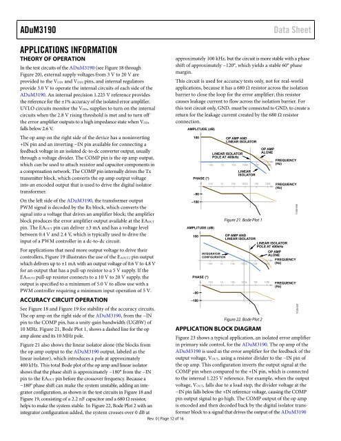
approximately 100 kHz, but the circuit is more stable with a phase<br />
shift of approximately −120°, which yields a stable 60° phase<br />
margin.<br />
This circuit is used for accuracy tests only, not for real-world<br />
applications, because it has a 680 Ω resistor across the isolation<br />
barrier to close the loop for the error amplifier; this resistor<br />
causes leakage current to flow across the isolation barrier. For<br />
this test circuit only, GND1 must be connected to GND2 to create a<br />
return for the leakage current created by the 680 Ω resistor<br />
connection.<br />
AMPLITUDE (dB)<br />
The op amp on the right side of the device has a noninverting<br />
100<br />
OP AMP AND<br />
+IN pin and an inverting −IN pin available for connecting a<br />
LINEAR ISOLATOR<br />
feedback voltage in an isolated dc-to-dc converter output, usually<br />
through a voltage divider. The COMP pin is the op amp output,<br />
which can be used to attach resistor and capacitor components in<br />
LINEAR ISOLATOR<br />
POLE AT 400kHz<br />
100 1k 10k 100k 1M<br />
OP AMP<br />
ALONE<br />
FREQUENCY<br />
10M (Hz)<br />
a compensation network. The COMP pin internally drives the Tx<br />
LINEAR<br />
transmitter block, which converts the op amp output voltage<br />
PHASE (°)<br />
ISOLATOR<br />
into an encoded output that is used to drive the digital isolator<br />
transformer.<br />
–90<br />
100 1k 10k 100k 1M 10M FREQUENCY<br />
(Hz)<br />
On the left side of the <strong>ADuM3190</strong>, the transformer output<br />
PWM signal is decoded by the Rx block, which converts the<br />
signal into a voltage that drives an amplifier block; the amplifier<br />
–180<br />
block produces the error amplifier output available at the EAOUT<br />
Figure 21. Bode Plot 1<br />
pin. The EAOUT pin can deliver ±3 mA and has a voltage level<br />
AMPLITUDE (dB)<br />
between 0.4 V and 2.4 V, which is typically used to drive the<br />
input of a PWM controller in a dc-to-dc circuit.<br />
100<br />
OP AMP AND<br />
LINEAR ISOLATOR<br />
LINEAR ISOLATOR<br />
For applications that need more output voltage to drive their<br />
controllers, Figure 19 illustrates the use of the EAOUT2 pin output<br />
which delivers up to ±1 mA with an output voltage of 0.6 V to 4.8 V<br />
for an output that has a pull-up resistor to a 5 V supply. If the<br />
INTEGRATOR<br />
CONFIGURATION<br />
100 1k 10k 100k<br />
POLE AT 400kHz<br />
OP AMP<br />
ALONE<br />
FREQUENCY<br />
1M 10M (Hz)<br />
EAOUT2 pull-up resistor connects to a 10 V to 20 V supply, the<br />
PHASE (°)<br />
output is specified to a minimum of 5.0 V to allow use with a<br />
PWM controller requiring a minimum input operation of 5 V.<br />
–90<br />
100 1k 10k 100k 1M 10M FREQUENCY<br />
(Hz)<br />
ACCURACY CIRCUIT OPERATION<br />
See Figure 18 and Figure 19 for stability of the accuracy circuits.<br />
–180<br />
The op amp on the right side of the <strong>ADuM3190</strong>, from the −IN<br />
pin to the COMP pin, has a unity-gain bandwidth (UGBW) of<br />
Figure 22. Bode Plot 2<br />
10 MHz. Figure 21, Bode Plot 1, shows a dashed line for the op<br />
APPLICATION BLOCK DIAGRAM<br />
amp alone and its 10 MHz pole.<br />
Figure 23 shows a typical application, an isolated error amplifier<br />
Figure 21 also shows the linear isolator alone (the blocks from<br />
in primary side control, for the <strong>ADuM3190</strong>. The op amp of the<br />
the op amp output to the <strong>ADuM3190</strong> output, labeled as the<br />
<strong>ADuM3190</strong> is used as the error amplifier for the feedback of the<br />
linear isolator), which introduces a pole at approximately<br />
output voltage, VOUT, using a resistor divider to the −IN pin of<br />
400 kHz. This total Bode plot of the op amp and linear isolator<br />
the op amp. This configuration inverts the output signal at the<br />
shows that the phase shift is approximately −180° from the −IN<br />
COMP pin when compared to the +IN pin, which is connected<br />
pin to the EAOUT pin before the crossover frequency. Because a<br />
to the internal 1.225 V reference. For example, when the output<br />
−180° phase shift can make the system unstable, adding an inte-<br />
voltage, VOUT, falls due to a load step, the divider voltage at the<br />
grator configuration, as shown in the test circuits in Figure 18 and −IN pin falls below the +IN reference voltage, causing the COMP<br />
Figure 19, consisting of a 2.2 nF capacitor and a 680 Ω resistor,<br />
pin output signal to go high. The COMP output of the op amp<br />
helps to make the system stable. In Figure 22, Bode Plot 2 with an is encoded and then decoded back by the digital isolator trans-<br />
integrator configuration added, the system crosses over 0 dB at<br />
former block to a signal that drives the output of the <strong>ADuM3190</strong><br />
<strong>Rev</strong>. 0 | Page 12 of 16<br />
11335-006<br />
11335-007


