

ADuM3190 (Rev. 0) - Analog Devices
ADuM3190 (Rev. 0) - Analog Devices
ADuM3190 (Rev. 0) - Analog Devices

Create successful ePaper yourself
Turn your PDF publications into a flip-book with our unique Google optimized e-Paper software.
<strong>ADuM3190</strong> Data Sheet<br />
Figure 25. Setting the Output Voltage<br />
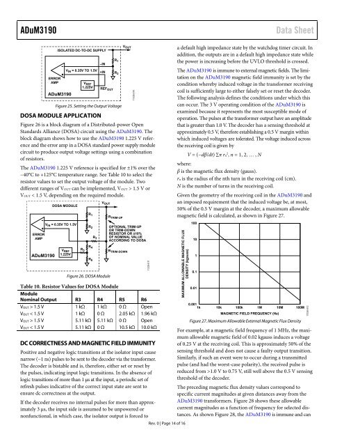
DOSA MODULE APPLICATION<br />
Figure 26 is a block diagram of a Distributed-power Open<br />
Standards Alliance (DOSA) circuit using the <strong>ADuM3190</strong>. The<br />
block diagram shows how to use the <strong>ADuM3190</strong> 1.225 V reference<br />
and the error amp in a DOSA standard power supply module<br />
circuit to produce output voltage settings using a combination<br />
of resistors.<br />
The <strong>ADuM3190</strong> 1.225 V reference is specified for ±1% over the<br />
−40°C to +125°C temperature range. See Table 10 to select the<br />
resistor values to set the output voltage of the module. Two<br />
different ranges of VOUT can be implemented, VOUT > 1.5 V or<br />
VOUT < 1.5 V, depending on the required module.<br />
ERROR<br />
AMP<br />
ERROR<br />
AMP<br />
<strong>ADuM3190</strong><br />
ISOLATED DC-TO-DC SUPPLY<br />
<strong>ADuM3190</strong><br />
DOSA MODULE<br />
V IN = 0.35V TO 1.5V<br />
V REF<br />
1.225V<br />
V IN = 0.35V TO 1.5V<br />
V REF<br />
1.225V<br />
R 5<br />
Figure 26. DOSA Module<br />
Table 10. Resistor Values for DOSA Module<br />
Module<br />
Nominal Output R3 R4 R5 R6<br />
VOUT > 1.5 V 1 kΩ 1 kΩ 0 Ω Open<br />
VOUT < 1.5 V 1 kΩ 0 Ω 2.05 kΩ 1.96 kΩ<br />
VOUT > 1.5 V 5.11 kΩ 5.11 kΩ 0 Ω Open<br />
VOUT < 1.5 V 5.11 kΩ 0 Ω 10.5 kΩ 10.0 kΩ<br />
DC CORRECTNESS AND MAGNETIC FIELD IMMUNITY<br />
Positive and negative logic transitions at the isolator input cause<br />
narrow (~1 ns) pulses to be sent to the decoder via the transformer.<br />
The decoder is bistable and is, therefore, either set or reset by<br />
the pulses, indicating input logic transitions. In the absence of<br />
logic transitions of more than 1 µs at the input, a periodic set of<br />
refresh pulses indicative of the correct input state are sent to<br />
ensure dc correctness at the output.<br />
If the decoder receives no internal pulses for more than approximately<br />
3 µs, the input side is assumed to be unpowered or<br />
nonfunctional, in which case, the isolator output is forced to<br />
R 1<br />
R 2<br />
R 4<br />
R 6<br />
R 3<br />
–IN<br />
+IN<br />
REF OUT<br />
V OUT<br />
R 1<br />
R 2<br />
R TRIM-UP<br />
V OUT<br />
R TRIM-DOWN<br />
11335-010<br />
OPTIONAL TRIM-UP<br />
OR TRIM-DOWN<br />
RESISTOR OR ±10%<br />
OF NOMINAL VALUE<br />
ACCORDING TO DOSA<br />
11335-011<br />
<strong>Rev</strong>. 0 | Page 14 of 16<br />
a default high impedance state by the watchdog timer circuit. In<br />
addition, the outputs are in a default high impedance state while<br />
the power is increasing before the UVLO threshold is crossed.<br />
The <strong>ADuM3190</strong> is immune to external magnetic fields. The limitation<br />
on the <strong>ADuM3190</strong> magnetic field immunity is set by the<br />
condition whereby induced voltage in the transformer receiving<br />
coil is sufficiently large to either falsely set or reset the decoder.<br />
The following analysis defines the conditions under which this<br />
can occur. The 3 V operating condition of the <strong>ADuM3190</strong> is<br />
examined because it represents the most susceptible mode of<br />
operation. The pulses at the transformer output have an amplitude<br />
that is greater than 1.0 V. The decoder has a sensing threshold at<br />
approximately 0.5 V, therefore establishing a 0.5 V margin within<br />
which induced voltages are tolerated. The voltage induced across<br />
the receiving coil is given by<br />
V = (−dβ/dt) ∑π rn 2 , n = 1, 2, … , N<br />
where:<br />
β is the magnetic flux density (gauss).<br />
rn is the radius of the nth turn in the receiving coil (cm).<br />
N is the number of turns in the receiving coil.<br />
Given the geometry of the receiving coil in the <strong>ADuM3190</strong> and<br />
an imposed requirement that the induced voltage be, at most,<br />
50% of the 0.5 V margin at the decoder, a maximum allowable<br />
magnetic field is calculated, as shown in Figure 27.<br />
MAXIMUM ALLOWABLE MAGNETIC FLUX<br />
DENSITY (kgauss)<br />
100<br />
10<br />
1<br />
0.1<br />
0.01<br />
0.001<br />
1k 10k 100k 1M 10M<br />
MAGNETIC FIELD FREQUENCY (Hz)<br />
Figure 27. Maximum Allowable External Magnetic Flux Density<br />
100M<br />
For example, at a magnetic field frequency of 1 MHz, the maximum<br />
allowable magnetic field of 0.02 kgauss induces a voltage<br />
of 0.25 V at the receiving coil. This is approximately 50% of the<br />
sensing threshold and does not cause a faulty output transition.<br />
Similarly, if such an event were to occur during a transmitted<br />
pulse (and had the worst-case polarity), the received pulse is<br />
reduced from >1.0 V to 0.75 V, still well above the 0.5 V sensing<br />
threshold of the decoder.<br />
The preceding magnetic flux density values correspond to<br />
specific current magnitudes at given distances away from the<br />
<strong>ADuM3190</strong> transformers. Figure 28 shows these allowable<br />
current magnitudes as a function of frequency for selected distances.<br />
As shown Figure 28, the <strong>ADuM3190</strong> is immune and can<br />
11335-012


