

ADuM3190 (Rev. 0) - Analog Devices
ADuM3190 (Rev. 0) - Analog Devices
ADuM3190 (Rev. 0) - Analog Devices

Create successful ePaper yourself
Turn your PDF publications into a flip-book with our unique Google optimized e-Paper software.
<strong>ADuM3190</strong> Data Sheet<br />
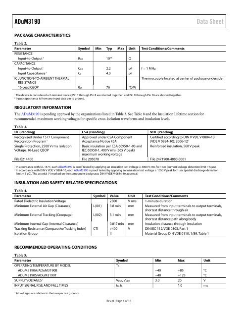
PACKAGE CHARACTERISTICS<br />
Table 2.<br />
Parameter<br />
RESISTANCE<br />
Symbol Min Typ Max Unit Test Conditions/Comments<br />
Input-to-Output1 RI-O 1013 CAPACITANCE<br />
Ω<br />
Input-to-Output1 CI-O 2.2 pF f = 1 MHz<br />
Input Capacitance 2 CI 4.0 pF<br />
IC JUNCTION-TO-AMBIENT THERMAL<br />
RESISTANCE<br />
Thermocouple located at center of package underside<br />
16-Lead QSOP θJA 76 °C/W<br />
1 The device is considered a 2-terminal device; Pin 1 through Pin 8 are shorted together, and Pin 9 through Pin 16 are shorted together.<br />
2 Input capacitance is from any input data pin to ground.<br />
REGULATORY INFORMATION<br />
The <strong>ADuM3190</strong> is pending approval by the organizations listed in Table 3. See Table 8 and the Insulation Lifetime section for<br />
recommended maximum working voltages for specific cross-isolation waveforms and insulation levels.<br />
Table 3.<br />
UL (Pending) CSA (Pending) VDE (Pending)<br />
Recognized Under 1577 Component<br />
Recognition Program1 Approved under CSA Component<br />
Certified according to DIN V VDE V 0884-10<br />
Acceptance Notice #5A<br />
(VDE V 0884-10): 2006-122 Single Protection, 2500 V rms Isolation<br />
Voltage, 16-Lead QSOP<br />
Basic insulation per CSA 60950-1-03 and<br />
IEC 60950-1, 400 V rms (565 V peak)<br />
maximum working voltage<br />
<strong>Rev</strong>. 0 | Page 4 of 16<br />
Reinforced insulation, 560 V peak<br />
File E214400 File 205078 File 2471900-4880-0001<br />
1 In accordance with UL 1577, each <strong>ADuM3190</strong> is proof tested by applying an insulation test voltage ≥ 3000 V rms for 1 sec (current leakage detection limit = 5 µA).<br />
2 In accordance with DIN V VDE V 0884-10, each <strong>ADuM3190</strong> is proof tested by applying an insulation test voltage ≥ 1050 V peak for 1 sec (partial discharge detection<br />
limit = 5 pC). The asterisk (*) marked on the component designates DIN V VDE V 0884-10 approval.<br />
INSULATION AND SAFETY RELATED SPECIFICATIONS<br />
Table 4.<br />
Parameter Symbol Value Unit Test Conditions/Comments<br />
Rated Dielectric Insulation Voltage 2500 V rms 1-minute duration<br />
Minimum External Air Gap (Clearance) L(I01) 3.8 min mm Measured from input terminals to output terminals,<br />
shortest distance through air<br />
Minimum External Tracking (Creepage) L(I02) 3.1 min mm Measured from input terminals to output terminals,<br />
shortest distance path along body<br />
Minimum Internal Gap (Internal Clearance) 0.017 min mm Insulation distance through insulation<br />
Tracking Resistance (Comparative Tracking Index) CTI >400 V DIN IEC 112/VDE 0303, Part 1<br />
Isolation Group II Material Group DIN VDE 0110, 1/89, Table 1<br />
RECOMMENDED OPERATING CONDITIONS<br />
Table 5.<br />
Parameter Symbol Min Max Unit<br />
OPERATING TEMPERATURE BY MODEL TA<br />
<strong>ADuM3190</strong>A/<strong>ADuM3190</strong>B −40 +85 °C<br />
<strong>ADuM3190</strong>S/<strong>ADuM3190</strong>T −40 +125 °C<br />
SUPPLY VOLTAGES 1 VDD1, VDD2 3.0 20 V<br />
INPUT SIGNAL RISE AND FALL TIMES tR, tF 1.0 ms<br />
1 All voltages are relative to their respective grounds.


