

ADuM3190 (Rev. 0) - Analog Devices
ADuM3190 (Rev. 0) - Analog Devices
ADuM3190 (Rev. 0) - Analog Devices

You also want an ePaper? Increase the reach of your titles
YUMPU automatically turns print PDFs into web optimized ePapers that Google loves.
Data Sheet <strong>ADuM3190</strong><br />
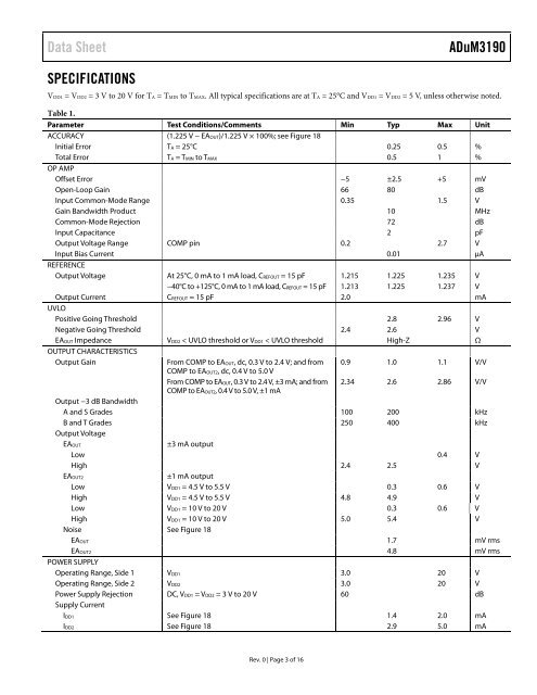
SPECIFICATIONS<br />
VDD1 = VDD2 = 3 V to 20 V for TA = TMIN to TMAX. All typical specifications are at TA = 25°C and VDD1 = VDD2 = 5 V, unless otherwise noted.<br />
Table 1.<br />
Parameter Test Conditions/Comments Min Typ Max Unit<br />
ACCURACY (1.225 V − EAOUT)/1.225 V × 100%; see Figure 18<br />
Initial Error TA = 25°C 0.25 0.5 %<br />
Total Error<br />
OP AMP<br />
TA = TMIN to TMAX 0.5 1 %<br />
Offset Error −5 ±2.5 +5 mV<br />
Open-Loop Gain 66 80 dB<br />
Input Common-Mode Range 0.35 1.5 V<br />
Gain Bandwidth Product 10 MHz<br />
Common-Mode Rejection 72 dB<br />
Input Capacitance 2 pF<br />
Output Voltage Range COMP pin 0.2 2.7 V<br />
Input Bias Current<br />
REFERENCE<br />
0.01 μA<br />
Output Voltage At 25°C, 0 mA to 1 mA load, CREFOUT = 15 pF 1.215 1.225 1.235 V<br />
−40°C to +125°C, 0 mA to 1 mA load, CREFOUT = 15 pF 1.213 1.225 1.237 V<br />
Output Current<br />
UVLO<br />
CREFOUT = 15 pF 2.0 mA<br />
Positive Going Threshold 2.8 2.96 V<br />
Negative Going Threshold 2.4 2.6 V<br />
EAOUT Impedance<br />
OUTPUT CHARACTERISTICS<br />
VDD2 < UVLO threshold or VDD1 < UVLO threshold High-Z Ω<br />
Output Gain From COMP to EAOUT, dc, 0.3 V to 2.4 V; and from<br />
COMP to EAOUT2, dc, 0.4 V to 5.0 V<br />
0.9 1.0 1.1 V/V<br />
Output −3 dB Bandwidth<br />
From COMP to EAOUT, 0.3 V to 2.4 V, ±3 mA; and from<br />
COMP to EAOUT2, 0.4 V to 5.0 V, ±1 mA<br />
2.34 2.6 2.86 V/V<br />
A and S Grades 100 200 kHz<br />
B and T Grades<br />
Output Voltage<br />
250 400 kHz<br />
EAOUT ±3 mA output<br />
Low 0.4 V<br />
High 2.4 2.5 V<br />
EAOUT2 ±1 mA output<br />
Low VDD1 = 4.5 V to 5.5 V 0.3 0.6 V<br />
High VDD1 = 4.5 V to 5.5 V 4.8 4.9 V<br />
Low VDD1 = 10 V to 20 V 0.3 0.6 V<br />
High VDD1 = 10 V to 20 V 5.0 5.4 V<br />
Noise See Figure 18<br />
EAOUT 1.7 mV rms<br />
EAOUT2<br />
POWER SUPPLY<br />
4.8 mV rms<br />
Operating Range, Side 1 VDD1 3.0 20 V<br />
Operating Range, Side 2 VDD2 3.0 20 V<br />
Power Supply Rejection<br />
Supply Current<br />
DC, VDD1 = VDD2 = 3 V to 20 V 60 dB<br />
IDD1 See Figure 18 1.4 2.0 mA<br />
IDD2 See Figure 18 2.9 5.0 mA<br />
<strong>Rev</strong>. 0 | Page 3 of 16


