CBM Progress Report 2006 - GSI
CBM Progress Report 2006 - GSI
CBM Progress Report 2006 - GSI

Create successful ePaper yourself
Turn your PDF publications into a flip-book with our unique Google optimized e-Paper software.
Detector Developments <strong>CBM</strong> <strong>Progress</strong> <strong>Report</strong> <strong>2006</strong><br />
Development of Microstrip Sensors for the <strong>CBM</strong> Silicon Tracking System<br />
J. M. Heuser and Chr. J. Schmidt, <strong>GSI</strong>, Darmstadt, Germany<br />
We have designed the first prototype of a silicon<br />
micro-strip sensor that can serve as a building block of<br />
detector modules for <strong>CBM</strong>’s Silicon Tracking System.<br />
Tracking Stations<br />
The tracking stations are planar arrangements of<br />
micro-strip sensors, grouped into several modules of either<br />
the same or different length, that cover at given positions<br />
downstream of the target the fiducial area approximately<br />
between 2.5 and 25 degrees polar angle. Figure 1 visualizes<br />
this station concept with a vertical orientation of the<br />
modules and the long direction of the strips perpendicular<br />
to the bending plane of the magnet for best momentum<br />
measurement. The first and smallest station may be<br />
as close as 30 cm to the target. The last and largest station<br />
will be in about one meter distance from the target.<br />
One of the key requirements of the Silicon Tracking System<br />
is a low-mass design to achieve momentum measurement<br />
with about 1% resolution. Silicon micro-strip detectors<br />
are compatible with a low-mass design as the sensors<br />
themselves are thin. With an appropriate module structure,<br />
active readout electronics with its cooling requirements<br />
and material involved may be avoided in the aperture.<br />
The strongly inhomogeneous track density profile<br />
makes a sectorized module structure necessary. Close to<br />
the beam line, a module must comprise sensors with short<br />
strips. Longer strips, realized either on single wafers or<br />
by chaining two or more sensors, can be employed in the<br />
regions further outside. Those different “sectors” must be<br />
read out individually. This may be realized by routing the<br />
strips’ analog signals from every sector through thin flat<br />
multi-line cables to front-end electronics at the periphery<br />
of the stations.<br />
Figure 1: Silicon micro-strip sensors arranged into modules<br />
of different lengths building up a tracking station.<br />
30<br />
Sensor Design<br />
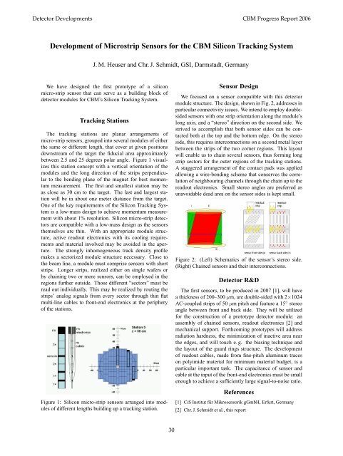
We focused on a sensor compatible with this detector<br />
module structure. The design, shown in Fig. 2, addresses in<br />
particular connectivity issues. We intend to employ doublesided<br />
sensors with one strip orientation along the module’s<br />
long axis, and a “stereo” direction on the second side. We<br />
strived to accomplish that both sensor sides can be contacted<br />
both at the top and the bottom edge. On the stereo<br />
side, this requires interconnections on a second metal layer<br />
between the strips of the two corner regions. This layout<br />
will enable us to chain several sensors, thus forming long<br />
strip sectors for the outer regions of the tracking stations.<br />
A staggered arrangement of the contact pads was applied<br />
allowing a wire-bonding scheme that conserves the correlation<br />
of neighbouring channels through the chain up to the<br />
readout electronics. Small stereo angles are preferred as<br />
unavoidable dead area on the sensor sides is kept small.<br />
Figure 2: (Left) Schematics of the sensor’s stereo side.<br />
(Right) Chained sensors and their interconnections.<br />
Detector R&D<br />
The first sensors, to be produced in 2007 [1], will have<br />
a thickness of 200–300 µm, are double-sided with 2×1024<br />
AC-coupled strips of 50 µm pitch and feature a 15 ◦ stereo<br />
angle between front and back side. They will be utilized<br />
for the construction of a prototype detector module: an<br />
assembly of chained sensors, readout electronics [2] and<br />
mechanical support. Forthcoming prototypes will address<br />
radiation hardness, the minimization of inactive area near<br />
the edges, and will touch e. g. the biasing technique and<br />
the layout of the guard rings structure. The development<br />
of readout cables, made from fine-pitch aluminum traces<br />
on polyimide material for minimum material budget, is a<br />
particular important task. The capacitance of sensor and<br />
cable at the input of the front-end electronics must be small<br />
enough to achieve a sufficiently large signal-to-noise ratio.<br />
References<br />
[1] CiS Institut für Mikrosensorik gGmbH, Erfurt, Germany<br />
[2] Chr. J. Schmidt et al., this report