- Page 1 and 2: FUJITSU SEMICONDUCTOR DATA SHEET Co
- Page 3 and 4: MB9B500 Series Multi-function Seri
- Page 5 and 6: Dual Timer (Two 32/16bit Down Count
- Page 7 and 8: PRODUCT LINEUP MB9B500 Series Memo
- Page 9 and 10: PIN ASSIGNMENT FPT-100P-M20/M23 VS
- Page 11 and 12: BGA-112P-M04 MB9B500 Series ・ Th
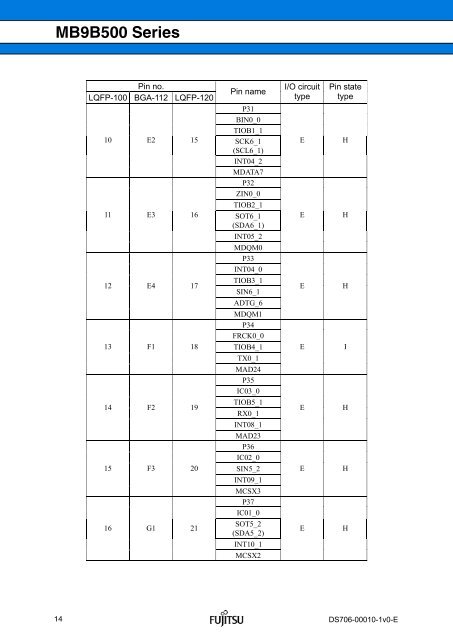
- Page 13: Pin no. LQFP-100 BGA-112 LQFP-120 D
- Page 17 and 18: Pin no. LQFP-100 BGA-112 LQFP-120 D
- Page 19 and 20: Pin no. LQFP-100 BGA-112 LQFP-120 D
- Page 21 and 22: Pin no. LQFP-100 BGA-112 LQFP-120 D
- Page 23 and 24: Pin no. LQFP-100 BGA-112 LQFP-120 D
- Page 25 and 26: MB9B500 Series SIGNAL DESCRIPTION
- Page 27 and 28: MB9B500 Series The number after the
- Page 29 and 30: MB9B500 Series The number after the
- Page 31 and 32: MB9B500 Series The number after the
- Page 33 and 34: MB9B500 Series The number after the
- Page 35 and 36: MB9B500 Series The number after the
- Page 37 and 38: MB9B500 Series The number after the
- Page 39 and 40: MB9B500 Series The number after the
- Page 41 and 42: MB9B500 Series Type Circuit Remarks
- Page 43 and 44: MB9B500 Series Type Circuit Remarks
- Page 45 and 46: MB9B500 Series PRECAUTIONS FOR HAN
- Page 47 and 48: MB9B500 Series Precautions for Pac
- Page 49 and 50: HANDLING DEVICES MB9B500 Series Po
- Page 51 and 52: HANDLING MB9BF500 MB9B500 Series H
- Page 53 and 54: MB9BF504/505/506 Block Diagram TRST
- Page 55 and 56: MB9B500 Series Memory Map(2) 0x2008
- Page 57 and 58: PIN STATUS IN EACH CPU STATE The te
- Page 59 and 60: Pin status type Power-on reset or l
- Page 61 and 62: Pin status type Function group Powe
- Page 63 and 64: MB9B500 Series 2. Absolute Maximum
- Page 65 and 66:
DC Characteristics The following ta
- Page 67 and 68:
MB9B500 Series (2) MB9BF504/505/506
- Page 69 and 70:
MB9B500 Series 2. Pin Characteristi
- Page 71 and 72:
MB9B500 Series (2) Sub Clock Input
- Page 73 and 74:
MB9B500 Series (7) External Bus Tim
- Page 75 and 76:
MB9B500 Series ・ NAND FLASH mode
- Page 77 and 78:
(8) Base Timer Input Timing ・ Tim
- Page 79 and 80:
SCK SOT SIN SCK SOT SIN V IH tF DS7
- Page 81 and 82:
S C K S O T S IN S C K S O T S IN V
- Page 83 and 84:
SCK SOT SIN SCK SOT SIN *2 VOH VO L
- Page 85 and 86:
SCK SOT SIN SCK SOT SIN VOH VOL MB9
- Page 87 and 88:
MB9B500 Series (11) Quadrature Posi
- Page 89 and 90:
MB9B500 Series (12) I 2 C timing (V
- Page 91 and 92:
MB9B500 Series (14) JTAG timing (Vc
- Page 93 and 94:
(Continued) MB9B500 Series The outp
- Page 95 and 96:
MB9B500 Series ・ Setting examples
- Page 97 and 98:
MB9B500 Series ・ Setting examples
- Page 99 and 100:
・Definition of 10-bit A/D Convert
- Page 101 and 102:
12bit A/D Converter This chapter sh
- Page 103 and 104:
・Definition of 12-bit A/D Convert
- Page 105 and 106:
MB9B500 Series *3 : The output driv
- Page 107 and 108:
(Continued) Figure 1 Low-Speed Load
- Page 109 and 110:
Flash Memory Write/Erase Characteri
- Page 111 and 112:
Power supply current (Sub timer mod
- Page 113 and 114:
PACKAGE DIMENSIONS 100-pin plastic
- Page 115 and 116:
(Continued) 120-pin plastic LQFP (F
- Page 117 and 118:
MAJOR CHANGES IN THIS EDITION Page
- Page 119 and 120:
DS706-00010-1v0-E MB9B500 Series 11