FM3 MB9B500 Series - Microcontrollers - Fujitsu
FM3 MB9B500 Series - Microcontrollers - Fujitsu
FM3 MB9B500 Series - Microcontrollers - Fujitsu

You also want an ePaper? Increase the reach of your titles
YUMPU automatically turns print PDFs into web optimized ePapers that Google loves.
<strong>MB9B500</strong> <strong>Series</strong><br />
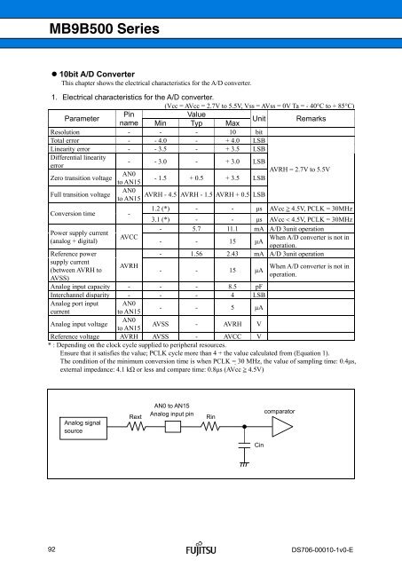
10bit A/D Converter<br />
This chapter shows the electrical characteristics for the A/D converter.<br />
1. Electrical characteristics for the A/D converter.<br />
(Vcc = AVcc = 2.7V to 5.5V, Vss = AVss = 0V Ta = - 40C to + 85C)<br />
Parameter<br />
Pin<br />
name Min<br />
Value<br />
Typ Max<br />
Unit Remarks<br />
Resolution - - - 10 bit<br />
Total error - - 4.0 - + 4.0 LSB<br />
Linearity error - - 3.5 - + 3.5 LSB<br />
Differential linearity<br />
error<br />
Zero transition voltage<br />
- - 3.0 - + 3.0 LSB<br />
AN0<br />
to AN15<br />
- 1.5 + 0.5 + 3.5 LSB<br />
AVRH = 2.7V to 5.5V<br />
Full transition voltage<br />
AN0<br />
AVRH - 4.5 AVRH - 1.5 AVRH + 0.5 LSB<br />
to AN15<br />
Conversion time -<br />
1.2 (*)<br />
3.1 (*)<br />
-<br />
-<br />
-<br />
-<br />
μs<br />
μs<br />
AVcc 4.5V, PCLK = 30MHz<br />
AVcc 4.5V, PCLK = 30MHz<br />
Power supply current<br />
(analog + digital)<br />
AVCC<br />
-<br />
-<br />
5.7<br />
-<br />
11.1<br />
15<br />
mA<br />
μA<br />
A/D 3unit operation<br />
When A/D converter is not in<br />
operation.<br />
Reference power<br />
- 1.56 2.43 mA A/D 3unit operation<br />
supply current<br />
(between AVRH to<br />
AVSS)<br />
AVRH<br />
- - 15 μA<br />
When A/D converter is not in<br />
operation.<br />
Analog input capacity - - - 8.5 pF<br />
Interchannel disparity - - - 4 LSB<br />
Analog port input<br />
current<br />
AN0<br />
to AN15<br />
- - 5 μA<br />
Analog input voltage<br />
AN0<br />
to AN15<br />
AVSS - AVRH V<br />
Reference voltage AVRH AVSS - AVCC V<br />
* : Depending on the clock cycle supplied to peripheral resources.<br />
Ensure that it satisfies the value; PCLK cycle more than 4 + the value calculated from (Equation 1).<br />
The condition of the minimum conversion time is when PCLK = 30 MHz, the value of sampling time: 0.4μs,<br />
external impedance: 4.1 kΩ or less and compare time: 0.8μs (AVcc 4.5V)<br />
92<br />
Analog signal<br />
source<br />
Rext<br />
AN0 to AN15<br />
Analog input pin<br />
Rin<br />
Cin<br />
comparator<br />
DS706-00010-1v0-E