Comparison of Thin-Film Aluminum Deposition - Berkeley Microlab
Comparison of Thin-Film Aluminum Deposition - Berkeley Microlab
Comparison of Thin-Film Aluminum Deposition - Berkeley Microlab

You also want an ePaper? Increase the reach of your titles
YUMPU automatically turns print PDFs into web optimized ePapers that Google loves.
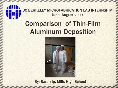
UC BERKELEY MICROFABRICATION LAB INTERNSHIP<br />
June- August 2009<br />
<strong>Comparison</strong> <strong>of</strong> <strong>Thin</strong>-<strong>Film</strong><br />
<strong>Aluminum</strong> <strong>Deposition</strong><br />
By: Sarah Ip, Mills High School
OBJECTIVE<br />
To compare thin-film aluminum deposition<br />
using:<br />
1) Resistivity<br />
2) Uniformity<br />
3) <strong>Deposition</strong> Rate
OUTLINE OF PROJECT<br />
- Cleaning Wafers & Oxide Growth<br />
- Sputtering<br />
- Novellus m2i Sputtering System<br />
- Edwards Auto 306DC and RF Sputter Coater<br />
-CPA Sputtering System<br />
-Evaporating<br />
- NRC Evaporator<br />
- Veeco 401 Vaccum System<br />
- Edwards eb3 Electron Beam Evaporator<br />
- Photolithography & Etching
NANO SPEC<br />
- thickness <strong>of</strong> oxide<br />
-reflectance<br />
T<br />
L C R<br />
F<br />
MEASUREMENT TOOLS & METHOD<br />
ASIQ<br />
-step measurement<br />
4 POINT PROBE<br />
- resistivity<br />
• systematic measurement <strong>of</strong> top, center,<br />
flat, left, right
CLEANING WAFERS & OXIDE GROWTH<br />
Sink 6<br />
- Piranha (Sulfuric Acid) with H 2 O 2<br />
- strong oxidizer- removes organic contamination<br />
- Creates some SiO 2<br />
- HF- dissolves SiO 2<br />
-remove metallic contamination<br />
Tystar 3<br />
-Recipe: 3WETOX<br />
-Temperature: 1000ºC<br />
-Time: 10 min 30 sec<br />
- Steam to oxidize Si faster than when dry
SPUTTERING<br />
Plasma (Argon gas) is ejected into the sputtering target, which releases clusters<br />
<strong>of</strong> aluminum particles onto the substrate (wafer).
EVAPORATING<br />
Metal is heated on through a filament, crucible, or metal plate. The evaporated metal is, then,<br />
condensed onto the substrate or wafer.<br />
For an electron beam evaporator, an electron beam bombards the metal which evaporates onto<br />
the substrate or wafer.
Evaporating<br />
Sputtering<br />
COMPARISON OF SPUTTERING AND EVAPORATING<br />
Advantages Disadvantages<br />
•consumes an efficient amount <strong>of</strong><br />
aluminum<br />
•more cost efficient (little Al per<br />
use)<br />
•versitile in ability to change<br />
metals<br />
•time comsuming<br />
•quick aluminum deposition •large machine (space is necessary)<br />
•expensive aluminum sheet for large<br />
target<br />
•difficult to change metal
Wafer Non-Uniformity<br />
(%)<br />
DATA ANALYSIS<br />
Bulk Resistivity<br />
(Ω-cm)<br />
Overall Time<br />
(Hr)<br />
<strong>Deposition</strong> Rate<br />
(Å/min)<br />
Novellus (25) 13.45 0.0414392 1/6 279.6<br />
Novellus (26) 11.06 0.02634984 1/6 550<br />
Edwards (13) 10.84 0.1126076 4 53.44<br />
CPA (2) 1.1 0.03399536 4 N/A<br />
NRC (5) 9.48 0.7033494 2 242.47<br />
V401 (12) 12.39 0.184477 2 251.8<br />
Edwards eb3 (31) 21.95 0.06602736 4 150<br />
•Non-Uniformity= (max-min)/avg<br />
•Bulk Resistivity= resistivity*thickness
DATA ANALYSIS<br />
Wafer Pre-thickness <strong>of</strong> Oxide Post-thickness <strong>of</strong><br />
Oxide<br />
Reflectance at 640 nm<br />
(% relative to Si)<br />
Novellus (25) 1084.4 1029.2 244.8<br />
Novellus (26) 1218.4 1041.8 226<br />
Edwards (13) 984.8 1007.6 217.2<br />
CPA (2) 999.4 1432.8 234.4<br />
NRC (5) 1001.4 1002.4 160.4<br />
V401 (12) 1004.8 1004.8 212.2<br />
Edwards eb3 (31) 1237.4 1193 196
OBSTACLES<br />
•When using NRC(1) and V401(2),<br />
1) a shadow formed, not allowing a even coat <strong>of</strong><br />
aluminum<br />
2) the aluminum became tinted with a golden color<br />
Solution: Re-do 2 wafers for each machine<br />
•When developing, some <strong>of</strong> the photo-resist did not develop<br />
properly, creating an inability for the CPA wafer to etch.<br />
Solution: Develop the wafer for a longer duration <strong>of</strong> time by<br />
developing twice
CONCLUSION<br />
•In a lab setting, evaporating is advantageous because it is cost efficient. Although<br />
evaporating is time consuming, labs are not mass producing, therefore, mitigating the<br />
problem <strong>of</strong> time.<br />
•Novellus outperforms in deposition rate, time, resistivity, and reflectance.<br />
•CPA produces the most uniform layer <strong>of</strong> aluminum.
ACKNOWLEDGEMNTS<br />
• Thank you, Jimmy Chang, for being a patient, helpful,<br />
and insightful mentor.<br />
• Thank you, Katalin Voros, for giving me the<br />
opportunity to be exposed to and enriched by the<br />
field <strong>of</strong> engineering.<br />
• Thank you for allowing me to learn from you: Sia<br />
Parsa, Rosemary Spivey, Daniel Queen, Lazlo Pethos,<br />
Xing Gao, Kim Chan, and <strong>Microlab</strong> members.<br />
• Thank you Marilyn Kushner for taking us to Semicon.