

AN-8027 — FAN480X PFC+PWM Combination Controller Application
AN-8027 — FAN480X PFC+PWM Combination Controller Application
AN-8027 — FAN480X PFC+PWM Combination Controller Application

Create successful ePaper yourself
Turn your PDF publications into a flip-book with our unique Google optimized e-Paper software.
<strong>AN</strong>-<strong>8027</strong><br />
60dB<br />
40dB<br />
20dB<br />
0dB<br />
-20dB<br />
-40dB<br />
Control-to-output<br />
Compensation<br />
Closed Loop Gain<br />
10Hz 100Hz 1kHz 10kHz 100kHz<br />
Figure 17. Current Loop Compensation<br />
f IZ<br />
f IC<br />
f IP<br />
1MHz<br />
(Design Example) Setting the crossover frequency<br />
as 7 kHz:<br />
vCS1 RCS1VBOUT <br />
v V 2fL IEA @ f f RAMP IC BOOST<br />
IC<br />
0.1387 0.66<br />
3 6<br />
2.55 2 7 10 524 10<br />
1 1<br />
RIC 17k<br />
6<br />
v 88100.66 CS1<br />
GMI<br />
<br />
v<br />
IEA @ f fIC<br />
1 1<br />
C 4nF<br />
2 / 3 17 10 2 7 10 / 3<br />
IC1<br />
3 3<br />
RICfC <br />
Setting the pole of the compensator at 70kHz,<br />
1 1<br />
C 0.13nF<br />
IC2<br />
3 3<br />
2 fIPRIC270101710 [STEP-9] PFC Voltage Loop Design<br />
Since F<strong>AN</strong>480X employs line feed-forward, the power<br />
stage transfer function becomes independent of the line<br />
voltage. Then, the low-frequency, small-signal, control-tooutput<br />
transfer function is obtained as:<br />
vˆ BOUT<br />
vˆ EA<br />
IBOUT KMAX<br />
1<br />
<br />
5 sCBOUT<br />
(37)<br />
where:<br />
vˆ BOUT<br />
vˆ IBOUT KMAX<br />
1<br />
<br />
5 sC<br />
(38)<br />
EA BOUT<br />
Proportional and integration (PI) control with highfrequency<br />
pole is typically used for compensation. The<br />
compensation zero (fVZ) introduces phase boost, while the<br />
high-frequency compensation pole (fVP) attenuates the<br />
switching ripple, as shown in Figure 18.<br />
© 2009 Fairchild Semiconductor Corporation www.fairchildsemi.com<br />
Rev. 1.0.2 • 6/21/13 10<br />
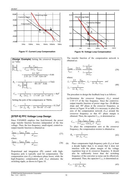
60dB<br />
40dB<br />
20dB<br />
0dB<br />
-20dB<br />
-40dB<br />
Closed-Loop Gain<br />
Control-to-Output<br />
fc<br />
Compensation<br />
1Hz 10Hz 100Hz 1kHz<br />
Figure 18. Voltage Loop Compensation<br />
10kHz<br />
The transfer function of the compensation network is<br />
obtained as:<br />
s<br />
1<br />
vˆ 2 f 2<br />
f<br />
<br />
vˆ s<br />
OUT s<br />
1 2<br />
f<br />
COMP VI VZ<br />
where:<br />
2.5<br />
fVI <br />
V<br />
GMV<br />
<br />
2 C ,<br />
1<br />
fVZ <br />
2<br />
R C<br />
and<br />
f<br />
VP<br />
VP<br />
BOUT VC1 VC VC1<br />
1<br />
<br />
2<br />
R C<br />
VC VC 2<br />
The procedure to design the feedback loop is as follows:<br />
(39)<br />
(40)<br />
(a) Determine the crossover frequency (fVC) around<br />
1/10~1/5 of the line frequency. Since the control-tooutput<br />
transfer function of power stage has -20 dB/dec<br />
slope and -90 o phase at the crossover frequency, as<br />
shown in Figure 18 as 0dB; it is necessary to place the<br />
zero of the compensation network (fVZ) around the<br />
crossover frequency so that 45 phase margin is<br />
obtained. Then, the capacitor CVC1 is determined as:<br />
GMV IBOUTKMAX2.5 CVC1<br />
2<br />
(41)<br />
5 CBOUT(2 fVC)<br />
VBOUT<br />
To place the compensation zero at the crossover<br />
frequency, the compensation resistor is obtained as:<br />
R<br />
VC<br />
1<br />
<br />
2<br />
f C<br />
VC VC1<br />
(42)<br />
(b) Place compensator high-frequency pole (fVP) at least<br />
a decade higher than fC to ensure that it does not<br />
interfere with the phase margin of the voltage<br />
regulation loop at its crossover frequency. It should<br />
also be sufficiently lower than the switching<br />
frequency of the converter so noise can be effectively<br />
attenuated. Then, the capacitor CVC2 is determined as:<br />
C<br />
VC2<br />
1<br />
<br />
2<br />
f R<br />
VP VC<br />
(43)


