

AN-8027 — FAN480X PFC+PWM Combination Controller Application
AN-8027 — FAN480X PFC+PWM Combination Controller Application
AN-8027 — FAN480X PFC+PWM Combination Controller Application

Create successful ePaper yourself
Turn your PDF publications into a flip-book with our unique Google optimized e-Paper software.
www.fairchildsemi.com<br />
<strong>AN</strong>-<strong>8027</strong><br />
F<strong>AN</strong>480X <strong>PFC+PWM</strong> <strong>Combination</strong> <strong>Controller</strong> <strong>Application</strong><br />
F<strong>AN</strong>4800AU / F<strong>AN</strong>4800AS / F<strong>AN</strong>4800C / F<strong>AN</strong>4800CS / F<strong>AN</strong>4801S / F<strong>AN</strong>4802S<br />
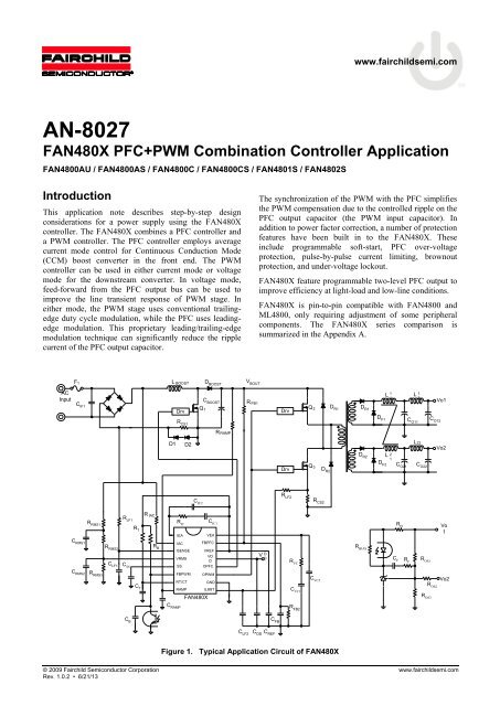
Introduction<br />
This application note describes step-by-step design<br />
considerations for a power supply using the F<strong>AN</strong>480X<br />
controller. The F<strong>AN</strong>480X combines a PFC controller and<br />
a PWM controller. The PFC controller employs average<br />
current mode control for Continuous Conduction Mode<br />
(CCM) boost converter in the front end. The PWM<br />
controller can be used in either current mode or voltage<br />
mode for the downstream converter. In voltage mode,<br />
feed-forward from the PFC output bus can be used to<br />
improve the line transient response of PWM stage. In<br />
either mode, the PWM stage uses conventional trailingedge<br />
duty cycle modulation, while the PFC uses leadingedge<br />
modulation. This proprietary leading/trailing-edge<br />
modulation technique can significantly reduce the ripple<br />
current of the PFC output capacitor.<br />
AC<br />
Input<br />
F1<br />
C IF1<br />
C RMS1<br />
C RMS2<br />
R RMS1<br />
R RMS3<br />
R RMS2<br />
R LF1<br />
C LF1 C SS<br />
C B<br />
R T<br />
C T<br />
R IAC<br />
R B<br />
L BOOST<br />
Drv<br />
R CS1<br />
D1 D2<br />
IEA<br />
IAC<br />
ISENSE<br />
VRMS<br />
SS<br />
C RAMP<br />
R IC<br />
FBPWM<br />
RT/CT<br />
RAMP<br />
Q1<br />
C IC2<br />
D BOOST<br />
C BOOST<br />
VEA<br />
FBPFC<br />
F<strong>AN</strong>480X<br />
C IC1<br />
VREF<br />
VD<br />
D<br />
OPFC<br />
OPWM<br />
GND<br />
ILIMIT<br />
RRAMP<br />
C LF2<br />
V BOUT<br />
R FB1<br />
The synchronization of the PWM with the PFC simplifies<br />
the PWM compensation due to the controlled ripple on the<br />
PFC output capacitor (the PWM input capacitor). In<br />
addition to power factor correction, a number of protection<br />
features have been built in to the F<strong>AN</strong>480X. These<br />
include programmable soft-start, PFC over-voltage<br />
protection, pulse-by-pulse current limiting, brownout<br />
protection, and under-voltage lockout.<br />
F<strong>AN</strong>480X feature programmable two-level PFC output to<br />
improve efficiency at light-load and low-line conditions.<br />
F<strong>AN</strong>480X is pin-to-pin compatible with F<strong>AN</strong>4800 and<br />
ML4800, only requiring adjustment of some peripheral<br />
components. The F<strong>AN</strong>480X series comparison is<br />
summarized in the Appendix A.<br />
© 2009 Fairchild Semiconductor Corporation www.fairchildsemi.com<br />
Rev. 1.0.2 • 6/21/13<br />
V D<br />
D<br />
C REF<br />
C DD<br />
C FB<br />
Drv<br />
Drv<br />
R LF2<br />
C VC1<br />
R FB2<br />
Q2<br />
Q3<br />
R CS2<br />
C VC2<br />
Figure 1. Typical <strong>Application</strong> Circuit of F<strong>AN</strong>480X<br />
R VC<br />
D R2<br />
D R1<br />
D R1<br />
D R2<br />
R BIAS<br />
D F1<br />
L 1<br />
1<br />
L 2<br />
1<br />
DF2 CO21 C F<br />
R D<br />
R F<br />
L 1<br />
2<br />
C O11<br />
L22<br />
C O22<br />
R OS1<br />
R OS3<br />
C O12<br />
R OS2<br />
Vo1<br />
Vo2<br />
Vo<br />
1<br />
Vo2
<strong>AN</strong>-<strong>8027</strong><br />
Functional Description<br />
Gain Modulator<br />
The gain modulator is the key block for PFC stage because<br />
it provides the reference to the current control error<br />
amplifier for the input current shaping, as shown in Figure<br />
2. The output current of gain modulator is a function of<br />
VEA, IAC, and VRMS. The gain of the gain modulator is<br />
given in the datasheet as a ratio between IMO and IAC with a<br />
given VRMS when VEA is saturated to HIGH. The gain is<br />
inversely proportional to VRMS 2 , as shown in Figure 3, to<br />
implement line feed-forward. This automatically adjusts<br />
the reference of current control error amplifier according<br />
to the line voltage such that the input power of PFC<br />
converter is not changed with line voltage.<br />
C RMS1<br />
C RMS2<br />
R RMS1<br />
V IN<br />
R RMS2<br />
R RMS3<br />
R IAC<br />
I AC<br />
ISENS<br />
E<br />
IA<br />
C<br />
VRMS<br />
VEA<br />
I L<br />
R<br />
M<br />
R<br />
M<br />
k<br />
x<br />
2<br />
Gain<br />
Modulator<br />
IEA<br />
I GI MO AC<br />
I Figure 2. Gain Modulator Block<br />
1<br />
G <br />
V<br />
2<br />
RMS<br />
V RMS-UVP<br />
K ( V 0.7)<br />
EA<br />
AC 2 MAX<br />
VRMSVEA V RMS<br />
Figure 3. Modulation Gain Characteristics<br />
( 0.7)<br />
To sense the RMS value of the line voltage, an averaging<br />
circuit with two poles is typically employed, as shown in<br />
Figure 2. The voltage of VRMS pin in normal PFC<br />
operation is given as:<br />
V V<br />
2R 2<br />
<br />
RMS 3<br />
RMS LINE<br />
<br />
RRMS1 RRMS2RRMS3 where VLINE is RMS value of line voltage.<br />
(1)<br />
However, once PFC stops switching operation, the<br />
junction capacitance of bridge diode is not discharged and<br />
VIN of Figure 2 is clamped at the peak of the line voltage.<br />
Then, the voltage of VRMS pin is given by:<br />
V V<br />
NS RMS 3<br />
RMS LINE<br />
RRMS1 RRMS2RRMS3 © 2009 Fairchild Semiconductor Corporation www.fairchildsemi.com<br />
Rev. 1.0.2 • 6/21/13 2<br />
2R<br />
Therefore, the voltage divider for VRMS should be<br />
designed considering the brownout protection trip point<br />
and minimum operation line voltage.<br />
V IN<br />
V RMS<br />
PFC runs PFC stops<br />
Figure 4. VRMS According to the PFC Operation<br />
The rectified sinusoidal signal is obtained by the current<br />
flowing into the IAC pin. The resistor RIAC should be large<br />
enough to prevent saturation of the gain modulator as:<br />
2VLINE.<br />
BO MAX<br />
G 159<br />
A<br />
(3)<br />
RIAC<br />
where VLINE.BO is the line voltage that trips brownout<br />
protection, G MAX is the maximum modulator gain when<br />
VRMS is 1.08 V (which can be found in the datasheet), and<br />
159 µA is the maximum output current of the gain<br />
modulator.<br />
Current and Voltage Control of Boost Stage<br />
As shown in Figure 5, the F<strong>AN</strong>480X employs two control<br />
loops for power factor correction: a current control loop<br />
and a voltage control loop. The current control loop shapes<br />
inductor current, as shown in Figure 6, based on the<br />
reference signal obtained at the IAC pin as:<br />
I R I R I G R<br />
(4)<br />
L CS1 MO M AC M<br />
(2)
<strong>AN</strong>-<strong>8027</strong><br />
C RMS1<br />
C RMS2<br />
R RMS1<br />
I AC<br />
I<br />
MO<br />
R<br />
R<br />
M<br />
CS1<br />
I L<br />
V IN<br />
R RMS2<br />
R RMS3<br />
R VC2<br />
R IAC<br />
I AC<br />
R F1<br />
ISENSE<br />
C F1<br />
IAC<br />
VRMS<br />
VEA<br />
R VC<br />
R VC1<br />
I L<br />
R CS1<br />
R M<br />
R M<br />
I MO<br />
+<br />
-<br />
2.5V<br />
Drive logic<br />
V O<br />
Figure 5. Gain Modulation Block<br />
IEA<br />
R IC<br />
CIC2 CIC1 VREF<br />
OPFC<br />
FBPFC<br />
Figure 6. Inductor Current Shaping<br />
The voltage control loop regulates PFC output voltage<br />
using internal error amplifier such that the FBPFC voltage<br />
is same as internal reference of 2.5 V.<br />
Brownout Protection<br />
F<strong>AN</strong>480X has a built-in internal brownout protection<br />
comparator monitoring the voltage of the VRMS pin. Once<br />
the VRMS pin voltage is lower than 1.05 V (0.9 V for<br />
F<strong>AN</strong>4802S), the PFC stage is shutdown to protect the<br />
system from over current. The F<strong>AN</strong>480X starts up the<br />
boost stage once the VRMS voltage increases above 1.9 V<br />
(1.65 V for F<strong>AN</strong>4802S).<br />
Two-Level PFC Output<br />
To improve system efficiency at low AC line voltage and<br />
light load condition, F<strong>AN</strong>480X provides two-level PFC<br />
output voltage. As shown in Figure 7, F<strong>AN</strong>480X monitors<br />
VEA and VRMS voltages to adjust the PFC output voltage.<br />
When VEA and VRMS are lower than the thresholds, an<br />
internal current source of 20 µA is enabled that flows<br />
through RFB2, increasing the voltage of the FBPFC pin.<br />
This causes the PFC output voltage to reduce when 20 µA<br />
is enabled, calculated as:<br />
R R<br />
V (2. 5- 20 μAR )<br />
FB1 FB2<br />
OPFC 2<br />
RFB2<br />
FB2<br />
R FB1<br />
R FB2<br />
(5)<br />
It is typical to set the second boost output voltage as<br />
340 V~300 V.<br />
© 2009 Fairchild Semiconductor Corporation www.fairchildsemi.com<br />
Rev. 1.0.2 • 6/21/13 3<br />
RFB1<br />
RFB2<br />
VBOUT<br />
FBPFC<br />
Oscillator<br />
2.5V<br />
VDD<br />
20uA<br />
-<br />
+<br />
1.95/2.45<br />
+<br />
-<br />
1.95/2.45<br />
For F<strong>AN</strong>4801S, VEA threshold is 2.8/3.35V<br />
Figure 7. Block of Two-Level PFC Output<br />
VRMS<br />
VEA<br />
The internal oscillator frequency of F<strong>AN</strong>480X is<br />
determined by the timing resistor and capacitor on the<br />
RT/CT pin. The frequency of the internal oscillator is<br />
given by:<br />
f<br />
OSC<br />
1<br />
<br />
0.56 R C 360C<br />
T T T<br />
Because the PWM stage of F<strong>AN</strong>480X generally uses a<br />
forward converter, it is required to limit the maximum duty<br />
cycle at 50%. To have a small tolerance of the maximum<br />
duty cycle, a frequency divider with toggle flip-flops is<br />
used, as illustrated in Figure 8. The operation frequency of<br />
PFC and PWM stage is one quarter (1/4) of the oscillator<br />
frequency. (For F<strong>AN</strong>4800CU, F<strong>AN</strong>4800CS, and<br />
F<strong>AN</strong>4802S, the operation frequencies for PFC and PWM<br />
stages are one quarter (1/4) and one half (1/2) of the<br />
oscillator frequency, respectively).<br />
The dead time for the PFC gate drive signal is determined<br />
by the equation:<br />
t 360C<br />
(7)<br />
DEAD T<br />
The dead time should be smaller than 2% of switching<br />
period to minimize line current distortion around line<br />
zero crossing.<br />
VREF<br />
RT/<br />
CT<br />
OSC<br />
T-FF<br />
T Q<br />
T-FF<br />
T Q<br />
OPWM (F<strong>AN</strong>4800CX, F<strong>AN</strong>4802S)<br />
Figure 8. Oscillator Configuration<br />
(6)<br />
OPFC, OPWM
<strong>AN</strong>-<strong>8027</strong><br />
RT/CT<br />
PFC dead time<br />
OPFC<br />
OPWM<br />
OPWM (F<strong>AN</strong>4800CX, F<strong>AN</strong>4802S)<br />
Figure 9. F<strong>AN</strong>480X Timing Diagram<br />
PWM Stage<br />
The PWM stage is capable of current-mode or voltagemode<br />
operation. In current-mode applications, the PWM<br />
ramp (RAMP) is usually derived directly from a current<br />
sensing resistor or current transformer in the primary of the<br />
output stage and is thereby representative of the current<br />
flowing in the converter’s output stage. ILIMIT, which<br />
provides cycle-by-cycle current limiting, is typically<br />
connected to RAMP in such applications.<br />
For voltage-mode operation, RAMP can be connected to a<br />
separate RC timing network to generate a voltage ramp<br />
against which FBPWM voltage is compared. Under these<br />
conditions, the use of voltage feed-forward from the PFC<br />
bus can be used for better line transient response.<br />
No voltage error amplifier is included in the PWM stage,<br />
as this function is generally performed by a programmable<br />
shunt regulator, such as KA431, in the secondary-side. To<br />
facilitate the design of opto-coupler feedback circuitry, an<br />
offset voltage is built into the inverting input of PWM<br />
comparator that allows FBPWM to command a zero<br />
percent duty cycle when its pin voltage is below 1.5 V.<br />
© 2009 Fairchild Semiconductor Corporation www.fairchildsemi.com<br />
Rev. 1.0.2 • 6/21/13 4<br />
V BOUT<br />
R RAMP<br />
C RAMP<br />
REF<br />
RAMP<br />
1.5V<br />
FBPWM<br />
Figure 10. PWM Ramp Generation Circuit<br />
PWM<br />
PWM Current Limit<br />
The ILIMIT pin is a direct input to the cycle-by-cycle<br />
current limiter for the PWM section. If the input voltage at<br />
this pin exceeds 1 V, the output of the PWM is disabled<br />
until the start of the next PWM clock cycle.<br />
VIN OK Comparator<br />
The VIN OK comparator monitors the output of the PFC<br />
stage and inhibits the PWM stage if this voltage is less<br />
than 2.4 V (96% of its nominal value). Once this voltage<br />
goes above 2.4 V, the PWM stage begins to soft-start.<br />
PWM Soft-Start (SS)<br />
PWM startup is controlled by the soft-start capacitor. A<br />
10 µA current source supplies the charging current for the<br />
soft-start capacitor. Startup of the PWM is prohibited until<br />
the soft-start capacitor voltage reaches 1.5 V.<br />
-<br />
+
<strong>AN</strong>-<strong>8027</strong><br />
Design Considerations<br />
In this section, a design procedure is presented using the<br />
schematic in Figure 11 as reference. A 300 W PC power<br />
supply application with universal input range is selected as<br />
Design Specifications<br />
a design example. The design specifications are<br />
summarized in the table below. The two-switch forward<br />
converter is used for DC-DC converter stage.<br />
Rated Voltage of Output 1 VOUT1 = 5 V PWM Stage Efficiency ηPWM = 0.86<br />
Rated Current of Output 1 IOUT1 = 9 A Hold-up Time tHLD = 20 ms<br />
Rated Voltage of Output 2 Vout2 = 12 V Minimum PFC Output Voltage 310 V<br />
Rated Current of Output 2 IOUT2 = 16.5 A Nominal PFC output voltage VO_PFC = 387 V<br />
Rated Voltage of Output 3 VOUT3 = -12 V PFC Output Voltage Ripple 12 VPP<br />
Rated Current of Output 3 IOUT3 = 0.8 A PFC Inductor Ripple Current dI = 40%<br />
Rated Voltage of Output 4 VOUT4 = 3.3 V AC Input Voltage Frequency fline = 50 ~ 60 Hz<br />
Rated Current of Output 4 IOUT4 = 13.5 A Switching Frequency fS = 65 kHz<br />
Rated Output Power PO = 300 W Total Harmonic Distortion α = 4%<br />
Line Voltage Range 85~264 VAC Magnetic Flux Density ΔB = 0.27 T<br />
Line Frequency 50 Hz Current Density Dcma = 400 C-m/A<br />
Brownout Protection Line Voltage 72 VAC PWM Maximum Duty Cycle Dmax = 0.35<br />
Overall Stage Efficiency η = 0.82 5-V Output Current Ripple ILo1 = 44%<br />
AC<br />
Input<br />
F1<br />
C IF1<br />
C RMS1<br />
C RMS2<br />
R RMS1<br />
R RMS3<br />
R RMS2<br />
R LF1<br />
C LF1 C SS<br />
C B<br />
R T<br />
C T<br />
R IAC<br />
R B<br />
L BOOST<br />
Drv<br />
R CS1<br />
D1 D2<br />
IEA<br />
IAC<br />
ISENSE<br />
VRMS<br />
SS<br />
C RAMP<br />
R IC<br />
FBPWM<br />
RT/CT<br />
RAMP<br />
Q1<br />
C IC2<br />
D BOOST<br />
C BOOST<br />
VEA<br />
FBPFC<br />
F<strong>AN</strong>480X<br />
C IC1<br />
VREF<br />
VD<br />
D<br />
OPFC<br />
OPWM<br />
GND<br />
ILIMIT<br />
RRAMP<br />
C LF2<br />
12-V Output Current Ripple ILo2 = 10%<br />
V BOUT<br />
R FB1<br />
© 2009 Fairchild Semiconductor Corporation www.fairchildsemi.com<br />
Rev. 1.0.2 • 6/21/13 5<br />
V D<br />
D<br />
C REF<br />
C DD<br />
C FB<br />
Drv<br />
Drv<br />
R LF2<br />
C VC1<br />
R FB2<br />
Q2<br />
Q3<br />
R CS2<br />
C VC2<br />
Figure 11. Reference Circuit for Design Example<br />
R VC<br />
D R2<br />
D R1<br />
D R1<br />
D R2<br />
R BIAS<br />
D F1<br />
L 1<br />
1<br />
L 2<br />
1<br />
DF2 CO21 C F<br />
R D<br />
R F<br />
L 1<br />
2<br />
C O11<br />
L22<br />
C O22<br />
R OS1<br />
R OS3<br />
C O12<br />
R OS2<br />
V o1<br />
V o2<br />
V o3<br />
V o4<br />
V o1<br />
V o2
<strong>AN</strong>-<strong>8027</strong><br />
[STEP-1] Define System Specifications<br />
Since the overall system is comprised of two stages (PFC<br />
and DC-DC), as shown in Figure 12, the input power and<br />
output power of the boost stage are given as:<br />
P<br />
P<br />
OUT<br />
IN<br />
(8)<br />
P<br />
<br />
P<br />
OUT<br />
BOUT<br />
(9)<br />
<br />
PWM<br />
where is the overall efficiency and PWM is the forward<br />
converter efficiency.<br />
The nominal output current of boost PFC stage is given as:<br />
I<br />
P<br />
OUT<br />
BOUT<br />
(10)<br />
P IN<br />
<br />
V<br />
PWM BOUT<br />
Boost<br />
PFC<br />
(Design Example)<br />
P BOUT<br />
I BOUT<br />
V BOUT<br />
Forward<br />
DC/DC<br />
Figure 12. Two-Stage Configuration<br />
P 300<br />
OUT<br />
P 366W<br />
IN<br />
0.82<br />
P 300<br />
OUT<br />
P 349W<br />
BOUT<br />
0.86<br />
PWM<br />
P<br />
300<br />
OUT<br />
IBOUT 0.9A<br />
V 0.86 387<br />
PWM BOUT<br />
[STEP-2] Frequency Setting<br />
P OUT<br />
V OUT<br />
The switching frequency is determined by the timing<br />
resistor and capacitor (RT and CT) as:<br />
f<br />
SW<br />
1 1<br />
<br />
4 0.56R<br />
C<br />
T T<br />
(11)<br />
It is typical to use a 470 pF~1 nF capacitor for 50~75 kHz<br />
switching frequency operation since the timing capacitor<br />
value determines the maximum duty cycle of PFC gate<br />
drive signal as:<br />
T<br />
D C f<br />
(12)<br />
MAX . PFC 1<br />
MIN<br />
OFF.<br />
TSW<br />
1 360 T SW<br />
(Design Example) Since the switching frequency is<br />
65 kHz, CT is selected as 1 nF. Then the maximum duty<br />
cycle of PFC gate drive signal is obtained as:<br />
DMAX . PFC 1 360 CT fSW<br />
0.98<br />
The timing resistor is determined as:<br />
1 1<br />
RT 4 0.56 f C<br />
6.9k<br />
© 2009 Fairchild Semiconductor Corporation www.fairchildsemi.com<br />
Rev. 1.0.2 • 6/21/13 6<br />
SW T<br />
[STEP-3] Line Sensing Circuit Design<br />
F<strong>AN</strong>480X senses the RMS value and instantaneous value of<br />
line voltage using the VRMS and IAC pins, respectively, as<br />
shown in Figure 13. The RMS value of the line voltage is<br />
obtained by an averaging circuit using low pass filter with<br />
two poles. Meanwhile, the instantaneous line voltage<br />
information is obtained by sensing the current flowing into<br />
the IAC pin through RIAC.<br />
C RMS1<br />
C RMS2<br />
R RMS1<br />
V IN<br />
R RMS2<br />
R RMS3<br />
R IAC<br />
I AC<br />
IA<br />
C<br />
I L<br />
VRMS<br />
V<br />
RMS<br />
Figure 13. Line Sensing Circuits<br />
V<br />
IN<br />
f p1<br />
f p2<br />
120/100Hz<br />
RMS sensing circuit should be designed considering the<br />
nominal operation range of line voltage and brownout<br />
protection trip point as:<br />
V V<br />
2R 2<br />
R R R <br />
RMS 3<br />
RMS UVL LINE. BO<br />
<br />
RMS1 RMS 2 RMS 3<br />
V V<br />
RMS UVH<br />
LINE. MIN<br />
2RRMS 3<br />
R RR RMS1 RMS 2 RMS 3<br />
(13)<br />
(14)<br />
where VRMS-UVL and VRMS-UVH are the brown OUT/IN<br />
thresholds of VRMS.<br />
It is typical to set RRMS2 as 10% of RRMS1. The poles of the<br />
low pass filter are given as:<br />
f<br />
P1<br />
f<br />
P2<br />
1<br />
<br />
2<br />
C R<br />
RMS1 RMS 2<br />
1<br />
<br />
2<br />
C R<br />
RMS 2 RMS 3<br />
(15)<br />
(16)<br />
To properly attenuate the twice line frequency ripple in
<strong>AN</strong>-<strong>8027</strong><br />
VRMS, it is typical to set the poles around 10~20 Hz.<br />
The resistor RIAC should be large enough to prevent<br />
saturation of the gain modulator as:<br />
2VLINE.<br />
BO MAX<br />
G 159<br />
A<br />
(17)<br />
RIAC<br />
where VLINE.BO is the brownout protection line voltage,<br />
G MAX is the maximum modulator gain when VRMS is 1.08 V<br />
(which can be found in the datasheet), and 159 µA is the<br />
maximum output current of the gain modulator.<br />
(Design Example) The brownout protection threshold is<br />
1.05 V (VRMS-UVL) and 1.9 V (VRMS-UVH), respectively.<br />
Then, the scaling down factor of the voltage divider is:<br />
RRMS3VRMSUVL <br />
RRMS1 RRMS2RRMS3 VLINE.<br />
BO 2 2<br />
1.05 <br />
0.0162<br />
72 2 2<br />
Then the startup of the PFC stage at the minimum line<br />
voltage is checked as:<br />
V 2R<br />
R RR LINE. MIN RMS 3<br />
RMS1 RMS 2 RMS 3<br />
85 2 0.0162 1.95 1.9V<br />
The resistors of the voltage divider network are selected<br />
as RRMS1=2 M, RRMS1=200 k, and RRMS1=36 k.<br />
To place the poles of the low pass filter at 15 Hz and<br />
22 Hz, the capacitors are obtained as:<br />
1 1<br />
CRMS1 53nF<br />
3<br />
2 f R 2 15 20010 P1 RMS 2<br />
1 1<br />
C 200nF<br />
RMS 2 3<br />
2 fP2RRMS3 2 22 36 10<br />
The condition for Resistor RIAC is:<br />
2VLINE . BO MAX 2 729 RIAC G 5.8M<br />
<br />
6 6<br />
1591015910 Therefore, 6 M resistor is selected for RIAC.<br />
[STEP-4] PFC Inductor Design<br />
The duty cycle of boost switch at the peak of line voltage is<br />
given as:<br />
D<br />
LP<br />
VBOUT2VLINE (18)<br />
V<br />
BOUT<br />
Then, the maximum current ripple of the boost inductor at<br />
the peak of line voltage for low line is given as:<br />
2VV2V1 LINE. MIN BOUT LINE<br />
IL (19)<br />
LBOOST VBOUT fSW<br />
The average of boost inductor current over one switching<br />
cycle at the peak of the line voltage for low line is given as:<br />
2POUT IL.<br />
AVG <br />
VLINE. MIN <br />
(20)<br />
Therefore, with a given current ripple factor<br />
(KRB=IL/ILAVG), the boost inductor value is obtained as:<br />
2<br />
VLINE. MIN VBOUT 2VLINE 1<br />
LBOOST<br />
<br />
KRB POUT VBOUT fSW<br />
The maximum current of boost inductor is given as:<br />
K 2P<br />
K<br />
I I (1 ) (1 )<br />
PK RB OUT<br />
RB<br />
L L. AVG<br />
2 VLINE. MIN <br />
2<br />
© 2009 Fairchild Semiconductor Corporation www.fairchildsemi.com<br />
Rev. 1.0.2 • 6/21/13 7<br />
(21)<br />
(22)<br />
(Design Example) With the ripple current specification<br />
(40%), the boost inductor is obtained as:<br />
L<br />
BOOST<br />
2<br />
VLINE. MIN VBOUT 2VLINE 1<br />
<br />
K P V f<br />
RB OUT BOUT SW<br />
2 3<br />
85 0.82 387 2 85<br />
10<br />
524H<br />
0.4 300 387 65<br />
The average of boost inductor current over one switching<br />
cycle at the peak of the line voltage for low line is<br />
obtained as:<br />
2POUT 2 300<br />
IL. AVG 6.09A<br />
V 850.82 LINE. MIN<br />
The maximum current of the boost inductor is given as:<br />
I<br />
2P<br />
K<br />
(1 )<br />
V <br />
2<br />
PK OUT RB<br />
L<br />
LINE. MIN<br />
2 300<br />
0.4<br />
(1 ) 7.31A<br />
85 0.82 2<br />
[STEP-5] PFC Output Capacitor Selection<br />
The output voltage ripple should be considered when<br />
selecting the PFC output capacitor. Figure 14 shows the<br />
twice line frequency ripple on the output voltage. With a<br />
given specification of output ripple, the condition for the<br />
output capacitor is obtained as:<br />
C<br />
BOUT<br />
I<br />
<br />
2<br />
f V<br />
BOUT<br />
LINE BOUT , RIPPLE<br />
(23)<br />
where IBOUT is nominal output current of boost PFC stage<br />
and VBOUT,RIPPLE is the peak-to-peak output voltage ripple<br />
specification.<br />
The hold-up time also should be considered when<br />
determining the output capacitor as:<br />
C<br />
BOUT<br />
P t<br />
<br />
V V<br />
BOUT HOLD<br />
2<br />
BOUT <br />
2<br />
BOUT , MIN<br />
(24)<br />
where PBOUT is nominal output power of boost PFC stage,<br />
tHOLD is the required holdup time, and VBOUT,MIN is the<br />
allowable minimum PFC output voltage during hold-up time.
<strong>AN</strong>-<strong>8027</strong><br />
I D, AVG<br />
I D<br />
I D, AVG I BOUT (1 cos(4 fLINE t))<br />
VBOUT<br />
V<br />
BOUT , RIPPLE<br />
IBOUT<br />
<br />
2<br />
f C<br />
Figure 14. PFC Output Voltage Ripple<br />
I BOUT<br />
LINE BOUT<br />
(Design Example) With the ripple specification of<br />
12 VPP, the capacitor should be:<br />
IBOUT<br />
0.9<br />
CBOUT239F 2 f V 25012 LINE BOUT , RIPPLE<br />
Since minimum allowable output voltage during one<br />
cycle line (20 ms) drop-outs is 310 V, the capacitor<br />
should be:<br />
PBOUTtHOLD 3<br />
2 349 2010 2<br />
OUT <br />
2<br />
OUT , MIN<br />
2 2<br />
387 310<br />
CBOUT260F V V<br />
Thus, 270 F capacitor is selected for the PFC output<br />
capacitor.<br />
[STEP-6] PFC Output Sensing Circuit<br />
To improve system efficiency at low line and light load<br />
condition, F<strong>AN</strong>480X provides two-level PFC output<br />
voltage. As shown in Figure 15, F<strong>AN</strong>480X monitors VEA<br />
and VRMS voltages to adjust the PFC output voltage.<br />
The PFC output voltage when 20 µA is enabled is given as:<br />
20μAR<br />
V V -<br />
2.5<br />
FB2<br />
BOUT 2 BOUT (1 )<br />
(25)<br />
It is typical second boost output voltage as 340 V~300 V.<br />
© 2009 Fairchild Semiconductor Corporation www.fairchildsemi.com<br />
Rev. 1.0.2 • 6/21/13 8<br />
RFB1<br />
RFB2<br />
VBOUT<br />
FBPFC<br />
2.5V<br />
VDD<br />
20uA<br />
-<br />
+<br />
1.95/2.45<br />
+<br />
-<br />
1.95/2.45<br />
For F<strong>AN</strong>4801S, VEA threshold is 2.8/3.35V.<br />
Figure 15. Two-Level PFC Output Block<br />
VRMS<br />
VEA<br />
The voltage divider network for the PFC output voltage<br />
sensing should be designed such that FBPFC voltage is<br />
2.5V at nominal PFC output voltage:<br />
R<br />
FB2<br />
VBOUT 2.5V<br />
RFB1RFB2 (Design Example) Assuming the second level of<br />
PFC output voltage is 347 V:<br />
R<br />
V 2.5<br />
(1 ) <br />
20 10<br />
BOUT 2<br />
FB2<br />
VBOUT<br />
<br />
6<br />
347 2.5<br />
(1 ) 12.9k<br />
6<br />
387 2010 13 k is selected for RFB2.<br />
R<br />
V<br />
(<br />
2.5<br />
387<br />
2.5<br />
1) R<br />
BOUT<br />
FB1 FB2<br />
3<br />
( 1) 1310 1999k<br />
2 M is selected for RFB1.<br />
(26)<br />
[STEP-7] PFC Current-Sensing Circuit Design<br />
Figure 16 shows the PFC compensation circuits. The first<br />
step in compensation network design is to select the currentsensing<br />
resistor of PFC converter considering the control<br />
window of voltage loop. Since line feed-forward is used in<br />
F<strong>AN</strong>480X, the output power is proportional to the voltage<br />
control error amplifier voltage as:<br />
V<br />
P ( V ) P <br />
V<br />
MAX EA<br />
BOUT EA BOUT SAT<br />
EA<br />
0.6<br />
0.6<br />
(27)<br />
where VEA SAT is 5.6 V and the maximum power limit of<br />
PFC is:<br />
V GR (28)<br />
2 MAX<br />
MAX LINE. BO M<br />
BOUT<br />
RIACRCS1 P
<strong>AN</strong>-<strong>8027</strong><br />
It is typical to set the maximum power limit of PFC stage<br />
around 1.2~1.5 of its nominal power such that the VEA is<br />
around 4~4.5 V at nominal output power. By adjusting the<br />
current-sensing resistor for PFC stage, the maximum<br />
power limit of PFC stage can be programmed.<br />
To filter out the current ripple of switching frequency, an<br />
RC filter is typically used for ISENSE pin. RLF1 should not<br />
be larger than 100 Ω and the cut-off frequency of filter<br />
should be 1/2~1/6 of the switching frequency.<br />
Diodes D1 and D2 are required to prevent over-voltage on<br />
the ISENSE pin due to the inrush current that might<br />
damage the IC. A fast recovery diode or ultra fast recovery<br />
diode is recommended.<br />
CRMS1<br />
CRMS2<br />
RRMS1<br />
VIN<br />
RRMS2<br />
RRMS3<br />
RVC2<br />
RIAC<br />
IAC<br />
RF1<br />
ISENS<br />
E<br />
CF1<br />
IA<br />
C<br />
VRMS<br />
VEA<br />
RV<br />
C<br />
RVC1<br />
IL<br />
RCS1<br />
RM<br />
R<br />
M<br />
IM<br />
O<br />
+<br />
-<br />
2.5V<br />
Drive<br />
logic<br />
Figure 16. Gain Modulation Block<br />
VO<br />
IEA<br />
RI<br />
C<br />
CIC2<br />
CIC1<br />
VREF<br />
OPFC<br />
FBPFC<br />
(Design Example) Setting the maximum power limit<br />
of PFC stage as 450W, the current sensing resistor is<br />
obtained as:<br />
R<br />
2 MAX<br />
2 3<br />
LINE. BO M<br />
CS1 MAX<br />
RIACPBOUT 6<br />
610450 RFB1<br />
RFB2<br />
V GR7295.710 0.098<br />
Thus, 0.1- resistor is selected.<br />
[STEP-8] PFC Current Loop Design<br />
The transfer function from duty cycle to the inductor<br />
current of boost power stage is given as:<br />
iL<br />
V<br />
<br />
d sL<br />
BOUT<br />
BOOST<br />
(29)<br />
The transfer function from the output of the current control<br />
error amplifier to the inductor current-sensing voltage is<br />
obtained as:<br />
v R V<br />
<br />
v V sL<br />
1 1 CS CS BOUT<br />
IEA RAMP BOOST<br />
(30)<br />
where VRAMP is the peak to peak voltage of ramp signal for<br />
current control PWM comparator, which is 2.55 V.<br />
The transfer function of the compensation circuit is given as:<br />
s<br />
1 vIEA2fII2f <br />
v s<br />
CS1<br />
s<br />
1 2<br />
f<br />
where:<br />
G<br />
1<br />
f , f <br />
and<br />
II<br />
MI<br />
2 CIC1 IZ<br />
2<br />
RIC CIC1<br />
1<br />
<br />
2<br />
R C<br />
IC IC 2<br />
© 2009 Fairchild Semiconductor Corporation www.fairchildsemi.com<br />
Rev. 1.0.2 • 6/21/13 9<br />
f<br />
IP<br />
IC<br />
IP<br />
The procedure to design the feedback loop is as follows:<br />
(31)<br />
(32)<br />
(a) Determine the crossover frequency (fIC) around<br />
1/10~1/6 of the switching frequency. Then calculate<br />
the gain of the transfer function of Equation (30) at<br />
crossover frequency as:<br />
vCS1 RCS1VBOUT <br />
v V 2fL IEA @ f f RAMP IC BOOST<br />
IC<br />
(33)<br />
(b) Calculate RIC that makes the closed loop gain unity at<br />
crossover frequency:<br />
R<br />
IC<br />
<br />
G<br />
MI<br />
v<br />
<br />
1<br />
CS1<br />
vIEA @ f fIC<br />
(34)<br />
(c) Since the control-to-output transfer function of power<br />
stage has -20 dB/dec slope and -90 o phase at the<br />
crossover frequency is 0 dB, as shown in Figure 17; it<br />
is necessary to place the zero of the compensation<br />
network (fIZ) around 1/3 of the crossover frequency so<br />
that more than 45 phase margin is obtained. Then the<br />
capacitor CIC1 is determined as:<br />
C<br />
IC1<br />
1<br />
<br />
R 2<br />
f / 3<br />
IC C<br />
(35)<br />
(d) Place compensator high-frequency pole (fCP) at least a<br />
decade higher than fIC to ensure that it does not<br />
interfere with the phase margin of the current loop at<br />
its crossover frequency.<br />
C<br />
IC 2<br />
1<br />
<br />
2<br />
f R<br />
IP IC<br />
(36)
<strong>AN</strong>-<strong>8027</strong><br />
60dB<br />
40dB<br />
20dB<br />
0dB<br />
-20dB<br />
-40dB<br />
Control-to-output<br />
Compensation<br />
Closed Loop Gain<br />
10Hz 100Hz 1kHz 10kHz 100kHz<br />
Figure 17. Current Loop Compensation<br />
f IZ<br />
f IC<br />
f IP<br />
1MHz<br />
(Design Example) Setting the crossover frequency<br />
as 7 kHz:<br />
vCS1 RCS1VBOUT <br />
v V 2fL IEA @ f f RAMP IC BOOST<br />
IC<br />
0.1387 0.66<br />
3 6<br />
2.55 2 7 10 524 10<br />
1 1<br />
RIC 17k<br />
6<br />
v 88100.66 CS1<br />
GMI<br />
<br />
v<br />
IEA @ f fIC<br />
1 1<br />
C 4nF<br />
2 / 3 17 10 2 7 10 / 3<br />
IC1<br />
3 3<br />
RICfC <br />
Setting the pole of the compensator at 70kHz,<br />
1 1<br />
C 0.13nF<br />
IC2<br />
3 3<br />
2 fIPRIC270101710 [STEP-9] PFC Voltage Loop Design<br />
Since F<strong>AN</strong>480X employs line feed-forward, the power<br />
stage transfer function becomes independent of the line<br />
voltage. Then, the low-frequency, small-signal, control-tooutput<br />
transfer function is obtained as:<br />
vˆ BOUT<br />
vˆ EA<br />
IBOUT KMAX<br />
1<br />
<br />
5 sCBOUT<br />
(37)<br />
where:<br />
vˆ BOUT<br />
vˆ IBOUT KMAX<br />
1<br />
<br />
5 sC<br />
(38)<br />
EA BOUT<br />
Proportional and integration (PI) control with highfrequency<br />
pole is typically used for compensation. The<br />
compensation zero (fVZ) introduces phase boost, while the<br />
high-frequency compensation pole (fVP) attenuates the<br />
switching ripple, as shown in Figure 18.<br />
© 2009 Fairchild Semiconductor Corporation www.fairchildsemi.com<br />
Rev. 1.0.2 • 6/21/13 10<br />
60dB<br />
40dB<br />
20dB<br />
0dB<br />
-20dB<br />
-40dB<br />
Closed-Loop Gain<br />
Control-to-Output<br />
fc<br />
Compensation<br />
1Hz 10Hz 100Hz 1kHz<br />
Figure 18. Voltage Loop Compensation<br />
10kHz<br />
The transfer function of the compensation network is<br />
obtained as:<br />
s<br />
1<br />
vˆ 2 f 2<br />
f<br />
<br />
vˆ s<br />
OUT s<br />
1 2<br />
f<br />
COMP VI VZ<br />
where:<br />
2.5<br />
fVI <br />
V<br />
GMV<br />
<br />
2 C ,<br />
1<br />
fVZ <br />
2<br />
R C<br />
and<br />
f<br />
VP<br />
VP<br />
BOUT VC1 VC VC1<br />
1<br />
<br />
2<br />
R C<br />
VC VC 2<br />
The procedure to design the feedback loop is as follows:<br />
(39)<br />
(40)<br />
(a) Determine the crossover frequency (fVC) around<br />
1/10~1/5 of the line frequency. Since the control-tooutput<br />
transfer function of power stage has -20 dB/dec<br />
slope and -90 o phase at the crossover frequency, as<br />
shown in Figure 18 as 0dB; it is necessary to place the<br />
zero of the compensation network (fVZ) around the<br />
crossover frequency so that 45 phase margin is<br />
obtained. Then, the capacitor CVC1 is determined as:<br />
GMV IBOUTKMAX2.5 CVC1<br />
2<br />
(41)<br />
5 CBOUT(2 fVC)<br />
VBOUT<br />
To place the compensation zero at the crossover<br />
frequency, the compensation resistor is obtained as:<br />
R<br />
VC<br />
1<br />
<br />
2<br />
f C<br />
VC VC1<br />
(42)<br />
(b) Place compensator high-frequency pole (fVP) at least<br />
a decade higher than fC to ensure that it does not<br />
interfere with the phase margin of the voltage<br />
regulation loop at its crossover frequency. It should<br />
also be sufficiently lower than the switching<br />
frequency of the converter so noise can be effectively<br />
attenuated. Then, the capacitor CVC2 is determined as:<br />
C<br />
VC2<br />
1<br />
<br />
2<br />
f R<br />
VP VC<br />
(43)
<strong>AN</strong>-<strong>8027</strong><br />
(Design Example) Setting the crossover frequency<br />
as 22 Hz:<br />
C<br />
G IK 2.5<br />
<br />
V<br />
MV BOUT MAX<br />
VC1<br />
2<br />
5 CBOUT(2 fVC)<br />
BOUT<br />
6<br />
7010 0.91.27 2.5<br />
6<br />
2<br />
20nF<br />
5 270 10<br />
(2 22)<br />
387<br />
1 1<br />
RVC 362k<br />
9<br />
2 f C 2 22 20 10<br />
VC VC1<br />
Setting the pole of the compensator at 120 Hz:<br />
1 1<br />
C 3.7nF<br />
VC2<br />
3<br />
2 fVPRVC212036210 [STEP-10] Transformer Design for PWM<br />
Stage<br />
Figure 19 shows the typical secondary-side circuit of<br />
forward converter for multi-output of PC power<br />
application.<br />
A common technique for winding multiple outputs with<br />
the same polarity sharing a common ground is to stack the<br />
secondary windings instead of winding each output<br />
winding separately. This approach improves the load<br />
regulation of the stacked outputs. The winding NS1 in<br />
Figure 19 must be sized to accommodate its output current,<br />
plus the current of the output (+12 V) stacked on top of it.<br />
To get tight regulation of 3.3 V output, magnetic amplifier<br />
(MAG-AMP) is used. The saturable core of MAG-AMP<br />
prevents the diode DREC from fully conducting by<br />
introducing high impedance until it is saturated. This<br />
allows the effective duty cycle of VREC to be controlled to<br />
be regulated the output voltage.<br />
N p<br />
N S<br />
1<br />
MAG<br />
AMP<br />
N S<br />
2<br />
D REC<br />
N S<br />
3<br />
V REC<br />
+<br />
-<br />
MAG AMP<br />
Control<br />
Additiona<br />
l LC filter<br />
Additiona<br />
l LC filter<br />
Additiona<br />
l LC filter<br />
Additiona<br />
l LC filter<br />
Figure 19. Typical Secondary-Side Circuit<br />
+12V<br />
+5V<br />
+3.3<br />
V<br />
-12V<br />
Once the core for the transformer is determined, the<br />
minimum number of turns for the transformer primary-side<br />
to avoid saturation is given by:<br />
V D<br />
MIN<br />
MIN BOUT MAX<br />
NP<br />
<br />
(44)<br />
Ae fSW B<br />
where Ae is the cross sectional area of the core in m 2 , fSW is<br />
the switching frequency, and B is the maximum flux<br />
density swing in Tesla for normal operation. B is<br />
typically 0.2-0.3 T for most power ferrite cores in the case<br />
of a forward converter.<br />
The turn ratio between the primary-side and secondaryside<br />
winding for the first output is determined by:<br />
MIN<br />
NP<br />
VBOUTDMAX n <br />
(45)<br />
NS1 ( VO1 VF<br />
1)<br />
where VF is the diode forward-voltage drop.<br />
Next, determine the proper integer for NS1 resulting in Np<br />
larger than Np min . Once the number of turns of the first<br />
output is determined, the number of turns of other output<br />
(n-th output) can be determined by:<br />
V V<br />
N N<br />
O( n) F ( n)<br />
S ( n) S1<br />
VO1VF1 © 2009 Fairchild Semiconductor Corporation www.fairchildsemi.com<br />
Rev. 1.0.2 • 6/21/13 11<br />
(46)<br />
The golden ratio between the secondary-side windings for<br />
the best regulation of 3.3 V, 5 V, and 12 V is known as<br />
2:3:7.<br />
(Design Example) The minimum PFC output voltage<br />
is 310 V and the maximum duty cycle of PWM<br />
controller is 50%. By adding 5% margin to the<br />
maximum duty cycle, DMAX=0.45 is used for<br />
transformer design. Assuming ERL35 (Ae=107 mm 2 )<br />
core is used and B=0.28, the minimum turns for the<br />
transformer primary side is obtained as:<br />
N<br />
MIN<br />
V D<br />
310 0.45<br />
72<br />
6<br />
3<br />
A f B 10710 65 10 0.28<br />
MIN BOUT MAX<br />
P<br />
e SW<br />
The turns ratio for 5 V output is obtained as:<br />
MIN<br />
NP<br />
VBOUTDMAX3100.45 n 25.6<br />
N ( V V) (5 0.45)<br />
S O F<br />
The number of turns for the primary-side winding is<br />
determined as:<br />
N n N 1 2 25.6 51.2 N<br />
MIN<br />
p S P<br />
N n N 3 25.6 76.8 N N 3<br />
MIN<br />
p S1 P S1<br />
Then, the turns ratio for 12-V output is obtained as:<br />
V V 12 0.7<br />
N N 3 6.99 7<br />
5 0.45<br />
O2 F2<br />
S2 VO1 VF1<br />
S1<br />
Therefore, the number of turns for each winding is<br />
obtained as:<br />
Np=78, NS1=3, NS2=7 (3+4 stack) and NS3=7.
<strong>AN</strong>-<strong>8027</strong><br />
[STEP-11] Coupled Inductor Design for the<br />
PWM Stage<br />
When the forward converter has more than one output, as<br />
shown in Figure 20, coupled inductors are usually employed<br />
to improve the cross regulation and to reduce the ripple.<br />
They are implemented by winding their separate coils on a<br />
single, common core. The turns ratio should be the same as<br />
the transformer turns ratio of the two outputs as:<br />
NS 2 NL<br />
2<br />
(47)<br />
N N<br />
S1 L1<br />
N<br />
p<br />
N S2<br />
N S1<br />
L 2<br />
N L2<br />
N L1<br />
L 1<br />
Figure 20. Coupled Inductor<br />
V N<br />
N<br />
POUT S1<br />
0<br />
0<br />
P<br />
V N<br />
N<br />
POUT S 2<br />
0<br />
P<br />
V N<br />
N<br />
D1<br />
D2<br />
N<br />
V V V<br />
POUT S1<br />
P<br />
L M<br />
L1<br />
L2<br />
N S1<br />
O2 O2 O1<br />
NS<br />
2<br />
N<br />
I I<br />
N S 2<br />
O2 O2<br />
NS1<br />
I SUM<br />
L LK<br />
L LK<br />
D1<br />
D2 N<br />
Normalized<br />
V O1<br />
I O1<br />
V O2<br />
I O2<br />
V O1<br />
I O2<br />
V N<br />
O2<br />
N IO2 Figure 21. Normalized Coupled Inductor Circuit<br />
VO2<br />
V O1<br />
One way to understand the operation of coupled inductor is<br />
to normalize the outputs to one output. Figure 21 shows<br />
how to normalize the second output (VO2) to the first<br />
output (VO1). The transformer and inductor turns are<br />
divided by NS2/NS1, the voltage and current are adjusted by<br />
NS2/NS1. It is assumed that the leakage inductances of the<br />
coupled inductor are much smaller than the magnetizing<br />
inductance and evenly distributed for each winding.<br />
The inductor value of the first output can be obtained by:<br />
L1 VO1( VO1 VF<br />
1)<br />
ISUM<br />
fSW ( PO 1PO2) ISUM<br />
(1 DMIN)<br />
(48)<br />
where:<br />
MIN<br />
VBOUT<br />
DMINDMAX VBOUT<br />
PO1PO2 ISUM<br />
<br />
V<br />
(49)<br />
© 2009 Fairchild Semiconductor Corporation www.fairchildsemi.com<br />
Rev. 1.0.2 • 6/21/13 12<br />
O1<br />
Then, the ripple current for each output is given as:<br />
IO1ISUM1 <br />
I 2 I<br />
(50)<br />
O1 O1<br />
IO2 ISUMNS1<br />
1<br />
(51)<br />
I 2 N I<br />
O2 S 2 O2<br />
(Design Example) The minimum duty cycle of<br />
PWM stage at nominal input (PFC output) voltage is:<br />
MIN<br />
VBOUT<br />
310<br />
DMINDMAX 0.45 0.36<br />
V<br />
389<br />
BOUT<br />
The sum of two normalize output current is:<br />
P P<br />
243<br />
O1 O2<br />
ISUM 48.6A<br />
VO1<br />
5<br />
Assuming 16% p-p ripple current in LSUM, the inductor<br />
for the first output is obtained as:<br />
V ( V V<br />
)<br />
O1 O1 F1<br />
L1DMIN ISUM<br />
fSW ( PO 1PO2) ISUM<br />
3<br />
6510 (5 9 12 16.5) 0.16<br />
(1 )<br />
5(5 0.45)<br />
(1 0.36) 6.9uH<br />
Then, the ripple current for each output is given as:<br />
IO1ISUM148.60.161 43%<br />
I 2 I 2 9<br />
O1 O1<br />
IO2 ISUMNS1 1 48.6 0.16 3 1<br />
<br />
10%<br />
I 2 N I 2 7 16.5<br />
O2 S 2 O2
<strong>AN</strong>-<strong>8027</strong><br />
[STEP-12] PWM Ramp Circuit Design<br />
For voltage-mode operation, the RAMP pin can be<br />
connected to a DC voltage through a resistor. When it is<br />
connected to the input of forward converter, ramp signal<br />
slope is automatically adjusted according to the input<br />
voltage providing line feed-forward operation. However, it<br />
can cause more power dissipation in the resistor. For better<br />
efficiency and lower standby power consumption, it is<br />
recommended to connect the RAMP pin to the VREF pin.<br />
CRAMP<br />
RRAMP<br />
VREF<br />
RAMP<br />
1.5V<br />
FBPWM<br />
PWM<br />
Figure 22. Ramp Generation Circuit for PWM<br />
It is typical to use 470 pF~1 nF capacitor on the RAMP<br />
pin and to have the peak of the ramp signal around 2~3 V.<br />
The peak of the ram voltage is given as:<br />
V<br />
1 V 1<br />
(52)<br />
C R 2 f<br />
PK REF<br />
RAMP<br />
RAMP RAMP SW<br />
(Design Example) Selecting CRAMP and RRAMP as 1 nF<br />
and 22 kΩ, the PWM ramp voltage is obtained as:<br />
V<br />
1 V 1<br />
<br />
C R 2 f<br />
PK REF<br />
RAMP<br />
RAMP RAMP SW<br />
1 7.5 1<br />
2.6V<br />
9<br />
3 3<br />
110 2210 2 6510 -<br />
+<br />
[STEP-13] Feedback Compensation Design<br />
for PWM Stage<br />
Figure 21 shows the typical cross-regulation compensation<br />
circuit configuration for multi-output converters. The<br />
small-signal characteristics of the compensation network is<br />
given as:<br />
RB<br />
1 s/ CZ1 1 s/<br />
CZ2<br />
( vO1vO2) 1 s / CP<br />
ROS1RDCFsROS2RDCFs where:<br />
© 2009 Fairchild Semiconductor Corporation www.fairchildsemi.com<br />
Rev. 1.0.2 • 6/21/13 13<br />
v<br />
<br />
<br />
<br />
FBPWM<br />
CP<br />
CZ1<br />
CZ 2<br />
1<br />
<br />
( R // R ) C<br />
1<br />
<br />
RC<br />
B1 B2 B<br />
F F<br />
1<br />
<br />
( R R ) C<br />
F OS 2 F<br />
VREF<br />
FBPWM<br />
RB<br />
RB1<br />
CB<br />
RD<br />
VO2 VO1<br />
ROS2<br />
RF CF<br />
KA431<br />
ROS1<br />
Figure 23. Feedback Compensation Circuit for<br />
PWM Stage<br />
(53)<br />
(54)<br />
ROS3<br />
The small signal equivalent circuit for control-to-output<br />
transfer function of the PWM power stage can be simplified<br />
as shown in Figure 24. The transfer function is fourth-order<br />
system because additional LC filters are used to meet the<br />
output voltage ripple specification. Therefore, it is<br />
recommended to use engineering software, such as PSPICE<br />
or Mathlab®, to design the feedback loop.<br />
NS1<br />
VBOUT<br />
<br />
NS<br />
2<br />
1<br />
V RAMP<br />
V FBPWM<br />
L M<br />
L LK<br />
L LK<br />
N CO21 C O11<br />
N L22 L L12<br />
N CO22 C O12<br />
N RL2 V N<br />
O2<br />
V O1<br />
R L1<br />
V O2<br />
N S1 :N S2<br />
Figure 24. Simplified Small Signal Equivalent Circuit for<br />
Control-to-Output Transfer Function
<strong>AN</strong>-<strong>8027</strong><br />
Design Summary<br />
<strong>Application</strong> Output Power Input Voltage Output Voltage / Output Current<br />
ATX Power 300 W 85~264 VAC 12 V / 16.5 A; 5 V / 9 A; -12 V / 0.8 A; 3.3 V / 13.5 A<br />
Features<br />
Meets 80+ specification<br />
F<strong>AN</strong>480X is fully pin-to-pin compatible with ML4800 and F<strong>AN</strong>4800 (needs a few parts modified)<br />
Switch-charge technique of gain modulator can provide better PF and lower THD<br />
Leading and trailing modulation technique for reduce output ripple<br />
Protections: OVP (Over-Voltage Protection), UVP (Under-Voltage Protection), OLP (Open-Loop Protection), and<br />
maximum current limit<br />
AC<br />
Input<br />
F1<br />
C IF1<br />
53nF<br />
C RMS1<br />
200n<br />
F<br />
C RMS2<br />
2M<br />
R RMS1<br />
200 K<br />
36 k<br />
R RMS3<br />
R RMS2<br />
R LF1<br />
C LF1 C SS<br />
0.47nF<br />
C B<br />
R T<br />
6.9 k<br />
C T<br />
1nF<br />
R IAC<br />
6 M<br />
R B<br />
5<br />
7.5k<br />
L BOOST<br />
FDA18N50<br />
R CS1<br />
D1 D2<br />
1nF<br />
R RAMP<br />
IEA<br />
IAC<br />
ISENSE<br />
VRMS<br />
SS<br />
C RAMP<br />
0.1<br />
R IC<br />
FBPWM<br />
RT/CT<br />
RAMP<br />
22k<br />
0.13nF CIC2 D BOOST<br />
BYC10600<br />
CBOOST Q1<br />
270uF<br />
17k 4nF<br />
VEA<br />
FBPFC<br />
F<strong>AN</strong>480X<br />
C IC1<br />
VREF<br />
VD<br />
D<br />
OPFC<br />
OPWM<br />
GND<br />
ILIMIT<br />
10<br />
C LF2<br />
V BOUT<br />
R FB1<br />
2M<br />
100 nF<br />
C DD<br />
10 k<br />
10 k<br />
V D<br />
D<br />
© 2009 Fairchild Semiconductor Corporation www.fairchildsemi.com<br />
Rev. 1.0.2 • 6/21/13 14<br />
C REF<br />
C FB<br />
FCP11N60<br />
R LF2<br />
R VC<br />
C VC1<br />
12.9k<br />
RFB2 Q2<br />
FCP11N60<br />
362k<br />
20nF<br />
FR157<br />
Q3<br />
DR2 R CS2<br />
3.7nF<br />
C VC2<br />
DR1 FR157<br />
Figure 25. Final Schematic of Design Example<br />
FYPF2006DN<br />
D R1<br />
D R2<br />
1.2 k<br />
C F<br />
100<br />
nF<br />
R D<br />
L 4<br />
1<br />
D F1<br />
L 1<br />
1<br />
L 2<br />
1<br />
DF2 STPS60L45CW<br />
SF34DG<br />
R F<br />
4.64 k<br />
L 3<br />
1<br />
C O31<br />
FR157<br />
32.4 k<br />
ROS1 11 k<br />
R OS3<br />
R OS2<br />
L 1<br />
1.8uH<br />
2<br />
C O11<br />
L22<br />
V o1<br />
V o2<br />
V o1<br />
CO12 1000uF<br />
V o2<br />
CO21 CO22 2200uF 1000uF<br />
L 4<br />
2<br />
DF2 FR157<br />
2200uF<br />
12V<br />
5V<br />
V o3<br />
220uF<br />
300<br />
2uH<br />
-12V<br />
L43<br />
C O21<br />
C O22<br />
10<br />
12V<br />
5V<br />
1 k<br />
1uF 10 k<br />
3.4 k<br />
3.3V<br />
5.45 k<br />
V o4
<strong>AN</strong>-<strong>8027</strong><br />
3<br />
2<br />
6,7<br />
Pin 1<br />
Winding Specification<br />
N1<br />
N5<br />
N3<br />
N2<br />
N4<br />
13<br />
8,9<br />
10,11,12<br />
14<br />
Margin Tape<br />
Margin Tape<br />
3mm 3mm<br />
BOBBIN-ERL35<br />
Figure 26. Forward Converter Transformer Structure<br />
© 2009 Fairchild Semiconductor Corporation www.fairchildsemi.com<br />
Rev. 1.0.2 • 6/21/13 15<br />
N5<br />
N4<br />
N3<br />
N2<br />
N1<br />
Mylar Tape 3T<br />
Mylar Tape 1T<br />
Mylar Tape 1T<br />
Mylar Tape 1T<br />
Mylar Tape 3T<br />
No Pin (s-f) Wire Turns Winding Method<br />
N1 3-2 0.6Ф 37 Ts Solenoid Winding<br />
Insulation: Mylar Tape t = 0.03 mm, 3 Layers<br />
N2 8,9-10,11,12 Copper-Foil 10 mil 3 Ts<br />
Insulation: Mylar Tape t = 0.03 mm, 1 Layers<br />
Copper-Foil Width<br />
18 mm<br />
N3 13-8,9 1.0Ф*4 4 Ts Solenoid Winding<br />
Insulation: Mylar Tape t = 0.03 mm, 1 Layers<br />
N4 10,11,12-14 0.4Ф 6 Ts Solenoid Winding<br />
Insulation: Mylar Tape t = 0.03 mm, 1 Layers<br />
N5 2-6,7 0.6Ф 37 Ts Solenoid Winding<br />
Insulation: Mylar Tape t = 0.03 mm, 3 Layers<br />
Core-ERL35<br />
Insulation: Mylar Tape t = 0.03 mm, 3 Layers<br />
Insulation: Copper-Foil Tape t = 0.05 mm-pin1 Open Loop<br />
Insulation: Mylar Tape t = 0.03 mm, 3 Layers<br />
Core: ERL35 (Ae=107 mm 2 )<br />
Bobbin: ERL35<br />
Inductance: 13 mH
<strong>AN</strong>-<strong>8027</strong><br />
Appendix A<br />
F<strong>AN</strong>480X Series Comparison Table of Relevant Parameters<br />
F<strong>AN</strong>4800 New Generation<br />
F<strong>AN</strong>4800AX<br />
New Generation<br />
F<strong>AN</strong>4800CX<br />
VDD Maximum Rating 20 V 30 V<br />
New Generation<br />
F<strong>AN</strong>4801S<br />
VDD OVP 17.9 V / Clamp 28 / Auto-Recover<br />
VCC UVLO 10 V / 13 V 9.3 / 11 V<br />
Two-Level PFC<br />
Output<br />
NO NO YES<br />
PFC Soft-Start NO YES<br />
Brownout NO YES<br />
New Generation<br />
F<strong>AN</strong>4802S<br />
PFC:PWM<br />
Frequency<br />
1:1 1:1 1:2 1:1 1:2<br />
Frequency Range 68 kHz~81 kHz 50 kHz~75 kHz<br />
Gate Clamp NO 16 V<br />
PFC Multiplier Traditional Switching Charge<br />
VINOK 2.25 V / 1.1 V 2.40 V / 1.15 V<br />
PWM Maximum Duty 42%~49% 49.5%~50%<br />
Startup Current 100 μA 30 μA<br />
Soft-Start Current 20 μA 10 μA<br />
PWM Comparator<br />
Level Shift<br />
1.0 V 1.5 V<br />
RAC 1~2 MΩ 5~8 MΩ<br />
MOSFET and Diode Reference Specification<br />
PFC MOSFETs<br />
Voltage Rating Part Number<br />
500 V FQP13N50C, FQPF13N50C, FDP18N50, FDPF18N50, FDA18N50, FDP20N50(T), FDPF20N50(T)<br />
600 V<br />
FCP11N60, FCPF11N60, FCP16N60, FCPF16N60, FCP20N60S, FCPF20N60S, FCA20N60S,<br />
FCP20N60, FCPF20N60<br />
Boost Diodes<br />
600 V FFP08H60S, FFPF10H60S, FFP08S60S, FPF08S60SN, BYC10600<br />
500 V<br />
600 V<br />
PWM MOSFETs<br />
FQP/PF9N50C, FQPF9N50C, FQP13N50C, FQPF13N50C, FQA13N50C, FDP18N50, FDPF18N50,<br />
FDP20N50(T), FDPF20N50(T)<br />
FCP11N60, FCPF11N60, FCP16N60, FCPF16N60, FCA16N60, FCP20N60S, FCPF20N60S,<br />
FCA20N60S, FCP20N60, FCPF20N60, FCA20N60<br />
© 2009 Fairchild Semiconductor Corporation www.fairchildsemi.com<br />
Rev. 1.0.2 • 6/21/13 16
<strong>AN</strong>-<strong>8027</strong><br />
References<br />
F<strong>AN</strong>480X <strong>—</strong> PFC/Forward PWM <strong>Controller</strong> Combo (F<strong>AN</strong>4800, F<strong>AN</strong>4801, F<strong>AN</strong>4802)<br />
<strong>AN</strong>-6004 <strong>—</strong> 500 W Power Factor Corrected (PFC) Design with F<strong>AN</strong>4810<br />
<strong>AN</strong>-6032 <strong>—</strong> F<strong>AN</strong>4800 Combo <strong>Controller</strong> <strong>Application</strong>s<br />
<strong>AN</strong>-42030 <strong>—</strong> Theory and <strong>Application</strong> of the ML4821 Average Current Mode PFC <strong>Controller</strong><br />
<strong>AN</strong>-42009 <strong>—</strong> ML4824 Combo <strong>Controller</strong> <strong>Application</strong>s<br />
ATX 300W 80+ Evaluation Board of F<strong>AN</strong>4800A+SG6520+FSQ0170<br />
DISCLAIMER<br />
FAIRCHILD SEMICONDUCTOR RESERVES THE RIGHT TO MAKE CH<strong>AN</strong>GES WITHOUT FURTHER NOTICE TO <strong>AN</strong>Y PRODUCTS<br />
HEREIN TO IMPROVE RELIABILITY, FUNCTION, OR DESIGN. FAIRCHILD DOES NOT ASSUME <strong>AN</strong>Y LIABILITY ARISING OUT OF<br />
THE APPLICATION OR USE OF <strong>AN</strong>Y PRODUCT OR CIRCUIT DESCRIBED HEREIN; NEITHER DOES IT CONVEY <strong>AN</strong>Y LICENSE<br />
UNDER ITS PATENT RIGHTS, NOR THE RIGHTS OF OTHERS.<br />
LIFE SUPPORT POLICY<br />
FAIRCHILD’S PRODUCTS ARE NOT AUTHORIZED FOR USE AS CRITICAL COMPONENTS IN LIFE SUPPORT DEVICES OR<br />
SYSTEMS WITHOUT THE EXPRESS WRITTEN APPROVAL OF THE PRESIDENT OF FAIRCHILD SEMICONDUCTOR<br />
CORPORATION.<br />
As used herein:<br />
1. Life support devices or systems are devices or systems<br />
which, (a) are intended for surgical implant into the body, or<br />
(b) support or sustain life, or (c) whose failure to perform<br />
when properly used in accordance with instructions for use<br />
provided in the labeling, can be reasonably expected to result<br />
in significant injury to the user.<br />
2. A critical component is any component of a life support device<br />
or system whose failure to perform can be reasonably<br />
expected to cause the failure of the life support device or<br />
system, or to affect its safety or effectiveness.<br />
© 2009 Fairchild Semiconductor Corporation www.fairchildsemi.com<br />
Rev. 1.0.2 • 6/21/13 17


