

AN-8027 — FAN480X PFC+PWM Combination Controller Application
AN-8027 — FAN480X PFC+PWM Combination Controller Application
AN-8027 — FAN480X PFC+PWM Combination Controller Application

You also want an ePaper? Increase the reach of your titles
YUMPU automatically turns print PDFs into web optimized ePapers that Google loves.
<strong>AN</strong>-<strong>8027</strong><br />
[STEP-1] Define System Specifications<br />
Since the overall system is comprised of two stages (PFC<br />
and DC-DC), as shown in Figure 12, the input power and<br />
output power of the boost stage are given as:<br />
P<br />
P<br />
OUT<br />
IN<br />
(8)<br />
P<br />
<br />
P<br />
OUT<br />
BOUT<br />
(9)<br />
<br />
PWM<br />
where is the overall efficiency and PWM is the forward<br />
converter efficiency.<br />
The nominal output current of boost PFC stage is given as:<br />
I<br />
P<br />
OUT<br />
BOUT<br />
(10)<br />
P IN<br />
<br />
V<br />
PWM BOUT<br />
Boost<br />
PFC<br />
(Design Example)<br />
P BOUT<br />
I BOUT<br />
V BOUT<br />
Forward<br />
DC/DC<br />
Figure 12. Two-Stage Configuration<br />
P 300<br />
OUT<br />
P 366W<br />
IN<br />
0.82<br />
P 300<br />
OUT<br />
P 349W<br />
BOUT<br />
0.86<br />
PWM<br />
P<br />
300<br />
OUT<br />
IBOUT 0.9A<br />
V 0.86 387<br />
PWM BOUT<br />
[STEP-2] Frequency Setting<br />
P OUT<br />
V OUT<br />
The switching frequency is determined by the timing<br />
resistor and capacitor (RT and CT) as:<br />
f<br />
SW<br />
1 1<br />
<br />
4 0.56R<br />
C<br />
T T<br />
(11)<br />
It is typical to use a 470 pF~1 nF capacitor for 50~75 kHz<br />
switching frequency operation since the timing capacitor<br />
value determines the maximum duty cycle of PFC gate<br />
drive signal as:<br />
T<br />
D C f<br />
(12)<br />
MAX . PFC 1<br />
MIN<br />
OFF.<br />
TSW<br />
1 360 T SW<br />
(Design Example) Since the switching frequency is<br />
65 kHz, CT is selected as 1 nF. Then the maximum duty<br />
cycle of PFC gate drive signal is obtained as:<br />
DMAX . PFC 1 360 CT fSW<br />
0.98<br />
The timing resistor is determined as:<br />
1 1<br />
RT 4 0.56 f C<br />
6.9k<br />
© 2009 Fairchild Semiconductor Corporation www.fairchildsemi.com<br />
Rev. 1.0.2 • 6/21/13 6<br />
SW T<br />
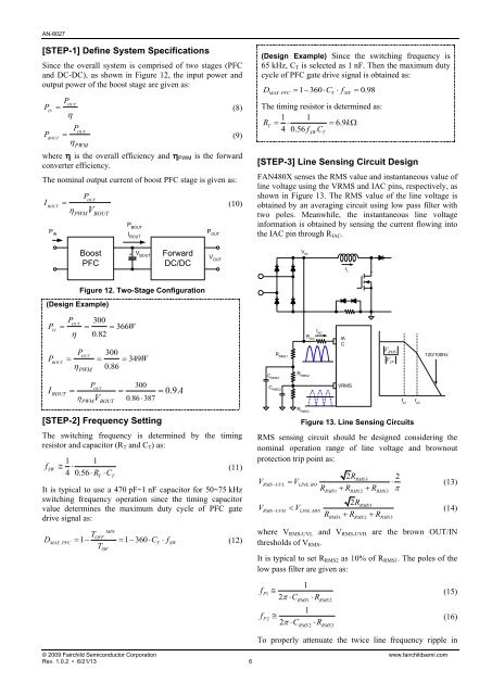
[STEP-3] Line Sensing Circuit Design<br />
F<strong>AN</strong>480X senses the RMS value and instantaneous value of<br />
line voltage using the VRMS and IAC pins, respectively, as<br />
shown in Figure 13. The RMS value of the line voltage is<br />
obtained by an averaging circuit using low pass filter with<br />
two poles. Meanwhile, the instantaneous line voltage<br />
information is obtained by sensing the current flowing into<br />
the IAC pin through RIAC.<br />
C RMS1<br />
C RMS2<br />
R RMS1<br />
V IN<br />
R RMS2<br />
R RMS3<br />
R IAC<br />
I AC<br />
IA<br />
C<br />
I L<br />
VRMS<br />
V<br />
RMS<br />
Figure 13. Line Sensing Circuits<br />
V<br />
IN<br />
f p1<br />
f p2<br />
120/100Hz<br />
RMS sensing circuit should be designed considering the<br />
nominal operation range of line voltage and brownout<br />
protection trip point as:<br />
V V<br />
2R 2<br />
R R R <br />
RMS 3<br />
RMS UVL LINE. BO<br />
<br />
RMS1 RMS 2 RMS 3<br />
V V<br />
RMS UVH<br />
LINE. MIN<br />
2RRMS 3<br />
R RR RMS1 RMS 2 RMS 3<br />
(13)<br />
(14)<br />
where VRMS-UVL and VRMS-UVH are the brown OUT/IN<br />
thresholds of VRMS.<br />
It is typical to set RRMS2 as 10% of RRMS1. The poles of the<br />
low pass filter are given as:<br />
f<br />
P1<br />
f<br />
P2<br />
1<br />
<br />
2<br />
C R<br />
RMS1 RMS 2<br />
1<br />
<br />
2<br />
C R<br />
RMS 2 RMS 3<br />
(15)<br />
(16)<br />
To properly attenuate the twice line frequency ripple in


