

AN-8027 — FAN480X PFC+PWM Combination Controller Application
AN-8027 — FAN480X PFC+PWM Combination Controller Application
AN-8027 — FAN480X PFC+PWM Combination Controller Application

Create successful ePaper yourself
Turn your PDF publications into a flip-book with our unique Google optimized e-Paper software.
<strong>AN</strong>-<strong>8027</strong><br />
I D, AVG<br />
I D<br />
I D, AVG I BOUT (1 cos(4 fLINE t))<br />
VBOUT<br />
V<br />
BOUT , RIPPLE<br />
IBOUT<br />
<br />
2<br />
f C<br />
Figure 14. PFC Output Voltage Ripple<br />
I BOUT<br />
LINE BOUT<br />
(Design Example) With the ripple specification of<br />
12 VPP, the capacitor should be:<br />
IBOUT<br />
0.9<br />
CBOUT239F 2 f V 25012 LINE BOUT , RIPPLE<br />
Since minimum allowable output voltage during one<br />
cycle line (20 ms) drop-outs is 310 V, the capacitor<br />
should be:<br />
PBOUTtHOLD 3<br />
2 349 2010 2<br />
OUT <br />
2<br />
OUT , MIN<br />
2 2<br />
387 310<br />
CBOUT260F V V<br />
Thus, 270 F capacitor is selected for the PFC output<br />
capacitor.<br />
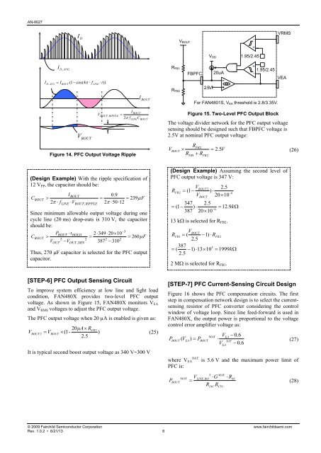
[STEP-6] PFC Output Sensing Circuit<br />
To improve system efficiency at low line and light load<br />
condition, F<strong>AN</strong>480X provides two-level PFC output<br />
voltage. As shown in Figure 15, F<strong>AN</strong>480X monitors VEA<br />
and VRMS voltages to adjust the PFC output voltage.<br />
The PFC output voltage when 20 µA is enabled is given as:<br />
20μAR<br />
V V -<br />
2.5<br />
FB2<br />
BOUT 2 BOUT (1 )<br />
(25)<br />
It is typical second boost output voltage as 340 V~300 V.<br />
© 2009 Fairchild Semiconductor Corporation www.fairchildsemi.com<br />
Rev. 1.0.2 • 6/21/13 8<br />
RFB1<br />
RFB2<br />
VBOUT<br />
FBPFC<br />
2.5V<br />
VDD<br />
20uA<br />
-<br />
+<br />
1.95/2.45<br />
+<br />
-<br />
1.95/2.45<br />
For F<strong>AN</strong>4801S, VEA threshold is 2.8/3.35V.<br />
Figure 15. Two-Level PFC Output Block<br />
VRMS<br />
VEA<br />
The voltage divider network for the PFC output voltage<br />
sensing should be designed such that FBPFC voltage is<br />
2.5V at nominal PFC output voltage:<br />
R<br />
FB2<br />
VBOUT 2.5V<br />
RFB1RFB2 (Design Example) Assuming the second level of<br />
PFC output voltage is 347 V:<br />
R<br />
V 2.5<br />
(1 ) <br />
20 10<br />
BOUT 2<br />
FB2<br />
VBOUT<br />
<br />
6<br />
347 2.5<br />
(1 ) 12.9k<br />
6<br />
387 2010 13 k is selected for RFB2.<br />
R<br />
V<br />
(<br />
2.5<br />
387<br />
2.5<br />
1) R<br />
BOUT<br />
FB1 FB2<br />
3<br />
( 1) 1310 1999k<br />
2 M is selected for RFB1.<br />
(26)<br />
[STEP-7] PFC Current-Sensing Circuit Design<br />
Figure 16 shows the PFC compensation circuits. The first<br />
step in compensation network design is to select the currentsensing<br />
resistor of PFC converter considering the control<br />
window of voltage loop. Since line feed-forward is used in<br />
F<strong>AN</strong>480X, the output power is proportional to the voltage<br />
control error amplifier voltage as:<br />
V<br />
P ( V ) P <br />
V<br />
MAX EA<br />
BOUT EA BOUT SAT<br />
EA<br />
0.6<br />
0.6<br />
(27)<br />
where VEA SAT is 5.6 V and the maximum power limit of<br />
PFC is:<br />
V GR (28)<br />
2 MAX<br />
MAX LINE. BO M<br />
BOUT<br />
RIACRCS1 P


