

AN-8027 — FAN480X PFC+PWM Combination Controller Application
AN-8027 — FAN480X PFC+PWM Combination Controller Application
AN-8027 — FAN480X PFC+PWM Combination Controller Application

Create successful ePaper yourself
Turn your PDF publications into a flip-book with our unique Google optimized e-Paper software.
<strong>AN</strong>-<strong>8027</strong><br />
Functional Description<br />
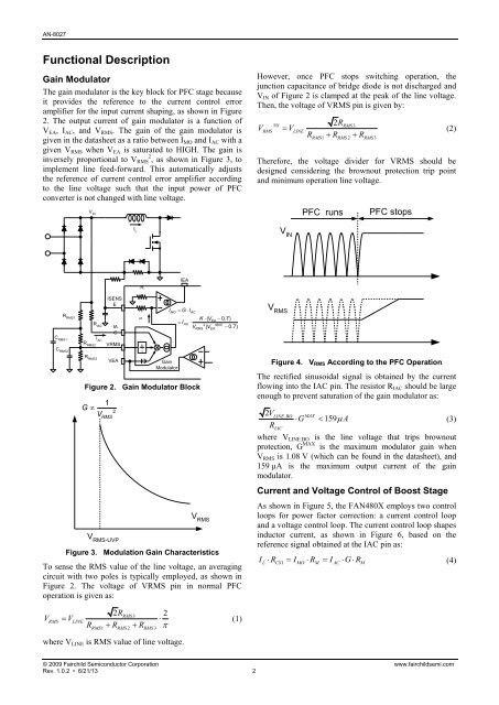
Gain Modulator<br />
The gain modulator is the key block for PFC stage because<br />
it provides the reference to the current control error<br />
amplifier for the input current shaping, as shown in Figure<br />
2. The output current of gain modulator is a function of<br />
VEA, IAC, and VRMS. The gain of the gain modulator is<br />
given in the datasheet as a ratio between IMO and IAC with a<br />
given VRMS when VEA is saturated to HIGH. The gain is<br />
inversely proportional to VRMS 2 , as shown in Figure 3, to<br />
implement line feed-forward. This automatically adjusts<br />
the reference of current control error amplifier according<br />
to the line voltage such that the input power of PFC<br />
converter is not changed with line voltage.<br />
C RMS1<br />
C RMS2<br />
R RMS1<br />
V IN<br />
R RMS2<br />
R RMS3<br />
R IAC<br />
I AC<br />
ISENS<br />
E<br />
IA<br />
C<br />
VRMS<br />
VEA<br />
I L<br />
R<br />
M<br />
R<br />
M<br />
k<br />
x<br />
2<br />
Gain<br />
Modulator<br />
IEA<br />
I GI MO AC<br />
I Figure 2. Gain Modulator Block<br />
1<br />
G <br />
V<br />
2<br />
RMS<br />
V RMS-UVP<br />
K ( V 0.7)<br />
EA<br />
AC 2 MAX<br />
VRMSVEA V RMS<br />
Figure 3. Modulation Gain Characteristics<br />
( 0.7)<br />
To sense the RMS value of the line voltage, an averaging<br />
circuit with two poles is typically employed, as shown in<br />
Figure 2. The voltage of VRMS pin in normal PFC<br />
operation is given as:<br />
V V<br />
2R 2<br />
<br />
RMS 3<br />
RMS LINE<br />
<br />
RRMS1 RRMS2RRMS3 where VLINE is RMS value of line voltage.<br />
(1)<br />
However, once PFC stops switching operation, the<br />
junction capacitance of bridge diode is not discharged and<br />
VIN of Figure 2 is clamped at the peak of the line voltage.<br />
Then, the voltage of VRMS pin is given by:<br />
V V<br />
NS RMS 3<br />
RMS LINE<br />
RRMS1 RRMS2RRMS3 © 2009 Fairchild Semiconductor Corporation www.fairchildsemi.com<br />
Rev. 1.0.2 • 6/21/13 2<br />
2R<br />
Therefore, the voltage divider for VRMS should be<br />
designed considering the brownout protection trip point<br />
and minimum operation line voltage.<br />
V IN<br />
V RMS<br />
PFC runs PFC stops<br />
Figure 4. VRMS According to the PFC Operation<br />
The rectified sinusoidal signal is obtained by the current<br />
flowing into the IAC pin. The resistor RIAC should be large<br />
enough to prevent saturation of the gain modulator as:<br />
2VLINE.<br />
BO MAX<br />
G 159<br />
A<br />
(3)<br />
RIAC<br />
where VLINE.BO is the line voltage that trips brownout<br />
protection, G MAX is the maximum modulator gain when<br />
VRMS is 1.08 V (which can be found in the datasheet), and<br />
159 µA is the maximum output current of the gain<br />
modulator.<br />
Current and Voltage Control of Boost Stage<br />
As shown in Figure 5, the F<strong>AN</strong>480X employs two control<br />
loops for power factor correction: a current control loop<br />
and a voltage control loop. The current control loop shapes<br />
inductor current, as shown in Figure 6, based on the<br />
reference signal obtained at the IAC pin as:<br />
I R I R I G R<br />
(4)<br />
L CS1 MO M AC M<br />
(2)


