

AN-8027 — FAN480X PFC+PWM Combination Controller Application
AN-8027 — FAN480X PFC+PWM Combination Controller Application
AN-8027 — FAN480X PFC+PWM Combination Controller Application

You also want an ePaper? Increase the reach of your titles
YUMPU automatically turns print PDFs into web optimized ePapers that Google loves.
<strong>AN</strong>-<strong>8027</strong><br />
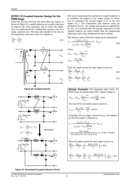
[STEP-11] Coupled Inductor Design for the<br />
PWM Stage<br />
When the forward converter has more than one output, as<br />
shown in Figure 20, coupled inductors are usually employed<br />
to improve the cross regulation and to reduce the ripple.<br />
They are implemented by winding their separate coils on a<br />
single, common core. The turns ratio should be the same as<br />
the transformer turns ratio of the two outputs as:<br />
NS 2 NL<br />
2<br />
(47)<br />
N N<br />
S1 L1<br />
N<br />
p<br />
N S2<br />
N S1<br />
L 2<br />
N L2<br />
N L1<br />
L 1<br />
Figure 20. Coupled Inductor<br />
V N<br />
N<br />
POUT S1<br />
0<br />
0<br />
P<br />
V N<br />
N<br />
POUT S 2<br />
0<br />
P<br />
V N<br />
N<br />
D1<br />
D2<br />
N<br />
V V V<br />
POUT S1<br />
P<br />
L M<br />
L1<br />
L2<br />
N S1<br />
O2 O2 O1<br />
NS<br />
2<br />
N<br />
I I<br />
N S 2<br />
O2 O2<br />
NS1<br />
I SUM<br />
L LK<br />
L LK<br />
D1<br />
D2 N<br />
Normalized<br />
V O1<br />
I O1<br />
V O2<br />
I O2<br />
V O1<br />
I O2<br />
V N<br />
O2<br />
N IO2 Figure 21. Normalized Coupled Inductor Circuit<br />
VO2<br />
V O1<br />
One way to understand the operation of coupled inductor is<br />
to normalize the outputs to one output. Figure 21 shows<br />
how to normalize the second output (VO2) to the first<br />
output (VO1). The transformer and inductor turns are<br />
divided by NS2/NS1, the voltage and current are adjusted by<br />
NS2/NS1. It is assumed that the leakage inductances of the<br />
coupled inductor are much smaller than the magnetizing<br />
inductance and evenly distributed for each winding.<br />
The inductor value of the first output can be obtained by:<br />
L1 VO1( VO1 VF<br />
1)<br />
ISUM<br />
fSW ( PO 1PO2) ISUM<br />
(1 DMIN)<br />
(48)<br />
where:<br />
MIN<br />
VBOUT<br />
DMINDMAX VBOUT<br />
PO1PO2 ISUM<br />
<br />
V<br />
(49)<br />
© 2009 Fairchild Semiconductor Corporation www.fairchildsemi.com<br />
Rev. 1.0.2 • 6/21/13 12<br />
O1<br />
Then, the ripple current for each output is given as:<br />
IO1ISUM1 <br />
I 2 I<br />
(50)<br />
O1 O1<br />
IO2 ISUMNS1<br />
1<br />
(51)<br />
I 2 N I<br />
O2 S 2 O2<br />
(Design Example) The minimum duty cycle of<br />
PWM stage at nominal input (PFC output) voltage is:<br />
MIN<br />
VBOUT<br />
310<br />
DMINDMAX 0.45 0.36<br />
V<br />
389<br />
BOUT<br />
The sum of two normalize output current is:<br />
P P<br />
243<br />
O1 O2<br />
ISUM 48.6A<br />
VO1<br />
5<br />
Assuming 16% p-p ripple current in LSUM, the inductor<br />
for the first output is obtained as:<br />
V ( V V<br />
)<br />
O1 O1 F1<br />
L1DMIN ISUM<br />
fSW ( PO 1PO2) ISUM<br />
3<br />
6510 (5 9 12 16.5) 0.16<br />
(1 )<br />
5(5 0.45)<br />
(1 0.36) 6.9uH<br />
Then, the ripple current for each output is given as:<br />
IO1ISUM148.60.161 43%<br />
I 2 I 2 9<br />
O1 O1<br />
IO2 ISUMNS1 1 48.6 0.16 3 1<br />
<br />
10%<br />
I 2 N I 2 7 16.5<br />
O2 S 2 O2


