

3-Phase BLDC Motor Control with Sensorless Back EMF ... - Freescale
3-Phase BLDC Motor Control with Sensorless Back EMF ... - Freescale
3-Phase BLDC Motor Control with Sensorless Back EMF ... - Freescale

Create successful ePaper yourself
Turn your PDF publications into a flip-book with our unique Google optimized e-Paper software.
<strong>Freescale</strong> Semiconductor<br />
Application Note<br />
3-<strong>Phase</strong> <strong>BLDC</strong> <strong>Motor</strong><br />
<strong>Control</strong> <strong>with</strong> <strong>Sensorless</strong><br />
<strong>Back</strong> <strong>EMF</strong> Zero Crossing<br />
Detection Using 56F80x<br />
Design of 3-<strong>Phase</strong> <strong>BLDC</strong> <strong>Motor</strong> <strong>Control</strong><br />
Application Based on the Software Development<br />
Kit<br />
Libor Prokop,<br />
Leos Chalupa<br />
1. Introduction<br />
This Application Note describes the design of a 3-phase<br />
sensorless <strong>BLDC</strong> motor drive <strong>with</strong> <strong>Back</strong>-<strong>EMF</strong> Zero Crossing. It<br />
is based on <strong>Freescale</strong>’s 56F80x family dedicated for motor<br />
control applications.<br />
The concept of the application is that of a speed-closed loop drive<br />
using <strong>Back</strong>-<strong>EMF</strong> Zero Crossing technique for position detection.<br />
It serves as an example of a sensorless <strong>BLDC</strong> motor control<br />
system using a Digital Signal <strong>Control</strong>ler (DSC) and SDK support.<br />
It also illustrates the usage of dedicated motor control on chip<br />
peripherals, software drivers and software libraries that are<br />
included in the SDK.<br />
This Application Note includes a description of the controller<br />
features, basic <strong>BLDC</strong> motor theory, system design concept,<br />
hardware implementation and software design including the PC<br />
master software visualization tool.<br />
Today more and more variable speed drives are designed into<br />
appliance products to increase product performance and system<br />
efficiency. The low dynamic drive, whereby the load or speed is<br />
changed quite slowly in comparison <strong>with</strong> the system mechanical<br />
time constant, is a solution for many common appliance<br />
applications because simple algorithms can perform the control<br />
tasks. Moreover, the necessary computing power can be<br />
© <strong>Freescale</strong> Semiconductor, Inc., 2001, 2005. All rights reserved.<br />
Contents<br />
AN1914<br />
Rev. 1, 11/2005<br />
1. Introduction .............................................1<br />
2. DSC Advantages and Features ...............2<br />
3. Target <strong>Motor</strong> Theory ..............................4<br />
4. System Design Concept ........................12<br />
5. <strong>Control</strong> Technique ................................16<br />
6. Hardware............................................... 29<br />
7. SW Design ............................................33<br />
8. SDK Implementation ............................46<br />
9. PC Master Software.............................. 48<br />
10. <strong>Control</strong>ler Usage .................................48<br />
11. Setting of SW parameters for other<br />
motor kits .........................................49<br />
12. References ...........................................54
DSC Advantages and Features<br />
minimized by using dedicated on chip peripheral modules (such as A/D converter, dedicated PWM outputs,<br />
input capture and output compare functions).<br />
Three phase Brushless DC (<strong>BLDC</strong>) motors are good candidates because of their high efficiency capability and<br />
easy to drive features. The disadvantage of this kind of motor is the fact that commutation of motor phases<br />
relies on its rotor position. Although the rotor position is usually sensed by sensors, there are applications that<br />
require sensorless control. Benefits of the sensorless solution are elimination of the position sensor and its<br />
connections between the control unit and the motor.<br />
The sensorless rotor position technique detects the zero crossing points of <strong>Back</strong>-<strong>EMF</strong> induced in the motor<br />
windings. The phase <strong>Back</strong>-<strong>EMF</strong> Zero Crossing points are sensed while one of the three phase windings is not<br />
powered. The obtained information is processed in order to commutate energized phase pair and control the<br />
phase voltage, using Pulse Width Modulation.<br />
This application note provides a fundamental mathematical method for modelling, torque calculation and<br />
control concept of the presented drive. The drive was developed in order to address simple applications (e.g.<br />
pumps, compressors, fans...) <strong>with</strong>in certain ranges of speed and load. Results from simulation show the drive<br />
behavior at different working conditions and better explain the drive strategy.<br />
2. DSC Advantages and Features<br />
The <strong>Freescale</strong> 56F80x family is well suited for digital motor control, combining the DSP’s calculation<br />
capability <strong>with</strong> MCU’s controller features on a single chip. These devices offer many dedicated peripherals<br />
like a Pulse Width Modulation (PWM) module, Analog-to-Digital Converter (ADC), Timers, communication<br />
peripherals (SCI, SPI, CAN), on-chip Flash and RAM. Generally, all family members are well suited for motor<br />
control application.<br />
The 56F805 device provides the following peripheral blocks:<br />
• Two Pulse Width Modulator modules (PWMA & PWMB), each <strong>with</strong> six PWM outputs, three Current<br />
Status inputs, and four Fault inputs, fault tolerant design <strong>with</strong> deadtime insertion, supports both<br />
Center- and Edge- aligned modes<br />
• Two twelve-bit, Analog-to-Digital Convertors (ADCs) that support simultaneous conversions <strong>with</strong><br />
dual 4-pin multiplexed inputs. ADC can be synchronized by PWM modules<br />
• Two Quadrature Decoders (Quad Dec0 & Quad Dec1), each <strong>with</strong> four inputs, or, alternatively, two<br />
additional Quad Timers (A & B)<br />
• Two dedicated General Purpose Quad Timers totalling 6 pins: Timer C <strong>with</strong> 2 pins and Timer D <strong>with</strong> 4<br />
pins<br />
• CAN 2.0 A/B Module <strong>with</strong> 2-pin ports used to transmit and receive<br />
• Two Serial Communication Interfaces (SCI0 & SCI1), each <strong>with</strong> two pins, or four additional GPIO<br />
lines<br />
• Serial Peripheral Interface (SPI), <strong>with</strong> configurable 4-pin port, or four additional GPIO lines<br />
• Computer Operating Properly (COP) timer<br />
• Two dedicated external interrupt pins<br />
• Fourteen dedicated General Purpose I/O (GPIO) pins, 18 multiplexed GPIO pins<br />
• External reset pin for hardware reset<br />
• External reset output pin for system reset<br />
• JTAG/On-Chip Emulation (OnCE)<br />
• Software-programmable, <strong>Phase</strong> Lock Loop-based frequency synthesizer for the core clock<br />
3-<strong>Phase</strong> <strong>BLDC</strong> <strong>Motor</strong> <strong>Control</strong>, Rev. 1<br />
2 <strong>Freescale</strong> Semiconductor<br />
Preliminary
Table 2-1. Memory Configuration<br />
56F801 56F803 56F805 56F807<br />
Program Flash 8188 x 16-bit 32252 x 16-bit 32252 x 16-bit 61436 x 16-bit<br />
Data Flash 2K x 16-bit 4K x 16-bit 4K x 16-bit 8K x 16-bit<br />
Program RAM 1K x 16-bit 512 x 16-bit 512 x 16-bit 2K x 16-bit<br />
Data RAM 1K x 16-bit 2K x 16-bit 2K x 16-bit 4K x 16-bit<br />
Boot Flash 2K x 16-bit 2K x 16-bit 2K x 16-bit 2K x 16-bit<br />
The <strong>BLDC</strong> motor control greatly benefits from the flexible PWM module, fast ADC and Quadrature Timer<br />
module. The PWM offers flexibility in its configuration, enabling efficient control of the <strong>BLDC</strong> motor.<br />
The PWM block has the following features:<br />
• Three complementary PWM signal pairs, or six independent PWM signals<br />
• Features of complementary channel operation<br />
• Deadtime insertion<br />
• Separate top and bottom pulse width correction via current status inputs or software<br />
• Separate top and bottom polarity control<br />
• Edge-aligned or center-aligned PWM signals<br />
• 15-bits of resolution<br />
• Half-cycle reload capability<br />
• Integral reload rates from one to 16<br />
• Individual software-controlled PWM output<br />
• Programmable fault protection<br />
• Polarity control<br />
• 20-mA current sink capability on each PWM pin<br />
• Write-protectable registers<br />
The PWM module is capable of providing the six PWM signals <strong>with</strong> bipolar switching (the diagonal power<br />
switches are driven by the same signal) and six-step <strong>BLDC</strong> commutation control where one motor phase is left<br />
unpowered so the <strong>Back</strong> <strong>EMF</strong> can be detected. The PWM duty cycle can be set asynchronously to the<br />
commutation of the motor phases using the channel swap feature.<br />
The Quadrature Timer feature set is as follows:<br />
• Four channels, independently programmable as input capture or output compare<br />
• Each channel has its own timebase source<br />
• Each of four channels can use any of four timer inputs<br />
• Rising edge, falling edge, or both edges input capture trigger<br />
• Set, clear, or toggle output capture action<br />
• Pulse Width Modulator (PWM) signal generation<br />
• Programmable clock sources and frequencies, including external clock<br />
3-<strong>Phase</strong> <strong>BLDC</strong> <strong>Motor</strong> <strong>Control</strong>, Rev. 1<br />
<strong>Freescale</strong> Semiconductor 3<br />
Preliminary
Target <strong>Motor</strong> Theory<br />
The Quadrature Timer provides the capability to precisely control the key sensorless <strong>BLDC</strong> events by<br />
providing the time base for zero crossing events and the output compare function for scheduling the<br />
commutation events.<br />
Dual Analog-to-Digital Converter (ADC) modules—four inputs on each has the following feature set:<br />
• Eight total analog inputs<br />
• 12-bit range<br />
• Monotonic over entire range <strong>with</strong> no missing codes<br />
• First channel on each ADC can be swapped <strong>with</strong> the alternate ADC<br />
• Can perform two simultaneous analog-to-digital conversions<br />
• Conversion time = 1.25 us<br />
• Contains programmable zero offset register<br />
• Generates interrupt on completion of conversion<br />
• Optional conversion interrupt is asserted when the analog voltage level exceeds, or<br />
• falls below, the value contained in the zero offset register<br />
• Output is in two’s complement or unsigned formats<br />
The Analog-to-Digital Converter is utilized to measure DC-bus voltage, DC-Bus current and the power module<br />
temperature. Its Hi/Lo level detection capability provides automatic detection of the over/under-voltage,<br />
over-current and over temperature protection (serviced in associated ISR).<br />
3. Target <strong>Motor</strong> Theory<br />
3.1 <strong>BLDC</strong> <strong>Motor</strong> Targeted by This Application<br />
The Brushless DC motor (<strong>BLDC</strong> motor) is also referred to as an electronically commuted motor. There are no<br />
brushes on the rotor and the commutation is performed electronically at certain rotor positions. The stator<br />
magnetic circuit is usually made from magnetic steel sheets. The stator phase windings are inserted in the slots<br />
(distributed winding) as shown in Figure 3-1 or it can be wound as one coil on the magnetic pole. The<br />
magnetization of the permanent magnets and their displacement on the rotor are chosen such a way that the<br />
<strong>Back</strong>-<strong>EMF</strong> (the voltage induced into the stator winding due to rotor movement) shape is trapezoidal. This<br />
allows the three phase voltage system (see Figure 3-2), <strong>with</strong> a rectangular shape, to be used to create a<br />
rotational field <strong>with</strong> low torque ripples.<br />
3-<strong>Phase</strong> <strong>BLDC</strong> <strong>Motor</strong> <strong>Control</strong>, Rev. 1<br />
4 <strong>Freescale</strong> Semiconductor<br />
Preliminary
Stator<br />
Stator winding<br />
(in slots)<br />
Shaft<br />
Rotor<br />
Air gap<br />
Figure 3-1. <strong>BLDC</strong> <strong>Motor</strong> - Cross Section<br />
<strong>BLDC</strong> <strong>Motor</strong> Targeted by This Application<br />
Permanent magnets<br />
The motor can have more then just one pole-pair per phase. This defines the ratio between the electrical<br />
revolution and the mechanical revolution. The <strong>BLDC</strong> motor shown has three pole-pairs per phase which<br />
represent three electrical revolutions per one mechanical revolution.<br />
The rectangular, easy to create, shape of applied voltage ensures the simplicity of control and drive. But the<br />
rotor position must be known at certain angles in order to align the applied voltage <strong>with</strong> the <strong>Back</strong>-<strong>EMF</strong>. The<br />
alignment between <strong>Back</strong>-<strong>EMF</strong> and commutation events is very important. In this condition the motor behaves<br />
as a DC motor and runs at the best working point. Thus simplicity of control and good performance make this<br />
motor a natural choice for low-cost and high-efficiency applications.<br />
Figure 3-2. Three <strong>Phase</strong> Voltage System<br />
electrical<br />
angle<br />
Figure 3-3 shows number of waveforms: the magnetic flux linkage, the phase <strong>Back</strong>-<strong>EMF</strong> voltage and the<br />
phase-to-phase <strong>Back</strong>-<strong>EMF</strong> voltage. The magnetic flux linkage can be measured; however in this case it was<br />
calculated by integrating the phase <strong>Back</strong>-<strong>EMF</strong> voltage, which was measured on the non-fed motor terminals of<br />
the <strong>BLDC</strong> motor. As can be seen, the shape of the <strong>Back</strong>-<strong>EMF</strong> is approximately trapezoidal and the amplitude<br />
is a function of the actual speed. During the speed reversal the amplitude is changed its sign and the phase<br />
sequence change too.<br />
3-<strong>Phase</strong> <strong>BLDC</strong> <strong>Motor</strong> <strong>Control</strong>, Rev. 1<br />
<strong>Freescale</strong> Semiconductor 5<br />
Preliminary
Target <strong>Motor</strong> Theory<br />
The filled areas in the tops of the phase <strong>Back</strong>-<strong>EMF</strong> voltage waveforms indicate the intervals where the<br />
particular phase power stage commutations occur. As can be seen, the power switches are cyclically<br />
commutated through the six steps. The crossing points of the phase <strong>Back</strong>-<strong>EMF</strong> voltages represent the natural<br />
commutation points. In normal operation the commutation is performed here. Some control techniques<br />
advance the commutation by a defined angle in order to control the drive above the PWM voltage control.<br />
Atop Btop Ctop<br />
Cbot Abot Bbot<br />
Ph. A Ph. B Ph. C<br />
Ph. A<br />
A-B<br />
Ph. B<br />
B-C<br />
3.2 3-<strong>Phase</strong> <strong>BLDC</strong> Power Stage<br />
<strong>Phase</strong> Magnetic Flux Linkage<br />
Ph. C<br />
C-A<br />
<strong>Phase</strong> <strong>Back</strong> <strong>EMF</strong><br />
3-<strong>Phase</strong> <strong>BLDC</strong> <strong>Motor</strong> <strong>Control</strong>, Rev. 1<br />
Speed reversal<br />
“Natural” commutation point<br />
Acting power switch in the power stage<br />
<strong>Phase</strong>-<strong>Phase</strong> <strong>Back</strong> <strong>EMF</strong><br />
Figure 3-3. <strong>BLDC</strong> <strong>Motor</strong> - <strong>Back</strong> <strong>EMF</strong> and Magnetic Flux<br />
The voltage for 3-phase <strong>BLDC</strong> motor is provided by a 3-phase power stage controlled by a DSC. The PWM<br />
module is usually implemented on a DSC to create desired control signals.<br />
A device <strong>with</strong> <strong>BLDC</strong> motor and power stage is shown in Figure 3-3.<br />
6 <strong>Freescale</strong> Semiconductor<br />
Preliminary<br />
Ps i_A<br />
Ps i_B<br />
Ps i_C<br />
Ui_A<br />
Ui_B<br />
Ui_C<br />
Ui_A B<br />
Ui_BC<br />
Ui_CA
3.3 Why <strong>Sensorless</strong> <strong>Control</strong>?<br />
3-<strong>Phase</strong> <strong>BLDC</strong> <strong>Motor</strong> <strong>Control</strong>, Rev. 1<br />
Power Stage - <strong>Motor</strong> System Model<br />
As explained in the previous section, the rotor position must be known in order to drive a Brushless DC motor.<br />
If any sensors are used to detect rotor position, then sensed information must be transferred to a control unit<br />
(see Figure 3-4). Therefore additional connections to the motor are necessary. This may not be acceptable for<br />
some applications. There are at least two reasons why you might want to eliminate the position sensors:<br />
• Inability to make additional connections between position sensors and the control unit<br />
• Cost of the position sensors and wiring<br />
~<br />
AC Line Voltage Power Stage<br />
=<br />
Speed<br />
Setting<br />
<strong>Control</strong> Signals<br />
<strong>Control</strong> Unit<br />
<strong>Freescale</strong> Semiconductor 7<br />
Preliminary<br />
M<br />
Figure 3-4. Classical System<br />
Position<br />
Feedback<br />
Position<br />
Sensors<br />
3.4 Power Stage - <strong>Motor</strong> System Model<br />
In order to explain and simulate the idea of <strong>Back</strong>-<strong>EMF</strong> sensing techniques a simplified mathematical model<br />
based on the basic circuit topology (see Figure 3-5) has been created.<br />
LOAD
Target <strong>Motor</strong> Theory<br />
Figure 3-5. Power Stage - <strong>Motor</strong> Topology<br />
The second goal of the model is to find how the motor characteristics depend on the switching angle. The<br />
switching angle is the angular difference between a real switching event and an ideal one (at the point where<br />
the phase to phase <strong>Back</strong>-<strong>EMF</strong> crosses zero).<br />
The motor-drive model consists of a normal three phase power stage plus a Brushless DC motor. The power<br />
for the system is provided by a voltage source (U d). Six semiconductor switches (S A/B/C t/b), controlled<br />
elsewhere, allow the rectangular voltage waveforms (see Figure 3-2) to be applied. The semiconductor<br />
switches and diodes are simulated as ideal devices. The natural voltage level of the whole model is put at one<br />
half of the DC bus voltage. This simplifies the mathematical expressions.<br />
3-<strong>Phase</strong> <strong>BLDC</strong> <strong>Motor</strong> <strong>Control</strong>, Rev. 1<br />
8 <strong>Freescale</strong> Semiconductor<br />
Preliminary
3.4.1 Mathematical Model<br />
The following set of equations is valid for the presented topology:<br />
where:<br />
u VA …u VC<br />
u A …u C<br />
u A<br />
u B<br />
u C<br />
u O<br />
⎛ C ⎞<br />
1<br />
= --⎜2u 3 VA – uVB – uVC + ⎟<br />
⎜ ∑ uix⎟ ⎝ ⎠<br />
3-<strong>Phase</strong> <strong>BLDC</strong> <strong>Motor</strong> <strong>Control</strong>, Rev. 1<br />
Power Stage - <strong>Motor</strong> System Model<br />
<strong>Freescale</strong> Semiconductor 9<br />
Preliminary<br />
x = A<br />
⎛ ⎞<br />
1<br />
= --⎜2u 3 VB – uVC – uVA + ∑ u ⎟<br />
⎜ ix⎟<br />
⎝ ⎠<br />
C<br />
x = A<br />
⎛ ⎞<br />
1<br />
= --⎜2u 3⎜<br />
VC – uVA – uVB + ∑ u ⎟<br />
ix⎟<br />
⎝ ⎠<br />
C<br />
⎛ ⎞<br />
1<br />
= --⎜ u<br />
3⎜<br />
∑ Vx – ∑ u ⎟<br />
ix⎟<br />
⎝ ⎠<br />
x = A<br />
0 = iA + iB + iC C<br />
x = A<br />
C<br />
x = A<br />
are “branch” voltages; the voltages between one power stage output and its virtual zero.<br />
are motor phase winding voltages.<br />
(EQ 3-1.)<br />
uiA…uiC are phase <strong>Back</strong>-<strong>EMF</strong> voltages induced in the stator winding.<br />
uO is the voltage between the central point of the star of motor winding and the power stage natural<br />
i A …i C<br />
zero<br />
are phase currents<br />
The equations (EQ 3-1.) can be written taking into account the motor phase resistance and the inductance. The<br />
mutual inductance between the two motor phase windings can be neglected because it is very small and has no<br />
significant effect for our abstraction level.<br />
where:<br />
uVA – uiA uVB – uiB uVC – uiC C<br />
⎛ ⎞<br />
1<br />
--⎜ u<br />
3 ∑ Vx – ∑ u ⎟<br />
diA –<br />
⎜ ix = R⋅i ⎟ A + L<br />
dt<br />
⎝ ⎠<br />
x = A<br />
C<br />
C<br />
x = A<br />
⎛ ⎞<br />
1<br />
--⎜ u<br />
3 ∑ Vx – ∑ u ⎟<br />
diB –<br />
⎜ ix = R⋅i ⎟ B + L<br />
dt<br />
⎝ ⎠<br />
x = A<br />
C<br />
C<br />
x = A<br />
⎛ ⎞<br />
1<br />
--⎜ u<br />
3 ∑ Vx – ∑ u ⎟<br />
diC –<br />
⎜ ix = R⋅i ⎟ C + L<br />
dt<br />
⎝ ⎠<br />
x = A<br />
R,L - motor phase resistance, inductance<br />
C<br />
x = A<br />
(EQ 3-2.)
Target <strong>Motor</strong> Theory<br />
The internal torque of the motor itself is defined as:<br />
where:<br />
T i<br />
C<br />
1<br />
dΨx = --- u<br />
ω ∑ ix ⋅ ix = ∑ ⋅ i<br />
dθ<br />
x<br />
(EQ 3-3.)<br />
x = A<br />
x = A<br />
T i - internal motor torque (no mechanical losses)<br />
ω,θ - rotor speed, rotor position<br />
x - phase index, it stands for A,B,C<br />
Ψ x - magnetic flux of phase winding x<br />
3-<strong>Phase</strong> <strong>BLDC</strong> <strong>Motor</strong> <strong>Control</strong>, Rev. 1<br />
10 <strong>Freescale</strong> Semiconductor<br />
Preliminary<br />
C<br />
It is important to understand how the <strong>Back</strong>-<strong>EMF</strong> can be sensed and how the motor behavior depends on the<br />
alignment of the <strong>Back</strong>-<strong>EMF</strong> to commutation events. This is explained in the next sections.<br />
3.5 <strong>Back</strong>-<strong>EMF</strong> Sensing<br />
The <strong>Back</strong>-<strong>EMF</strong> sensing technique is based on the fact that only two phases of a DC Brushless motor are<br />
connected at a time (see Figure 3-2), so the third phase can be used to sense the <strong>Back</strong>-<strong>EMF</strong> voltage.<br />
Let us assume the situation when phases A and B are powered and phase C is non-fed. No current is going<br />
through this phase. This is described by the following conditions:<br />
SAb, SBt ← are energized<br />
u VA<br />
i A<br />
1<br />
--u<br />
1<br />
= +−<br />
2 d,<br />
u -- VB = ± u<br />
2 d<br />
= – iB, iC = 0,<br />
diC = 0<br />
uiA + uiB + uiC = 0<br />
The branch voltage C can be calculated when considering the above conditions:<br />
u VC<br />
(EQ 3-1.)<br />
3<br />
= --u<br />
2 iC<br />
(EQ 3-2.)<br />
As shown in Figure 3-5, the branch voltage of phase C can be sensed between the power stage output C and<br />
the zero voltage level. Thus the <strong>Back</strong>-<strong>EMF</strong> voltage is obtained and the zero crossing can be recognized.<br />
The general expressions can also be found:<br />
u Vx<br />
There are two necessary conditions which must be met:<br />
3<br />
= --u<br />
2 ixwherex= ABC , ,<br />
(EQ 3-3.)<br />
• Top and bottom switch (in diagonal) have to be driven <strong>with</strong> the same PWM signal<br />
• No current is going through the non-fed phase used to sense the <strong>Back</strong>-<strong>EMF</strong><br />
Figure 3-6 shows branch and motor phase winding voltages during a 0-360°electrical interval. Shaded<br />
rectangles designate the validity of the equation (EQ 3-3.). In other words, the <strong>Back</strong>-<strong>EMF</strong> voltage can be<br />
sensed during designated intervals.
3.6 <strong>Back</strong>-<strong>EMF</strong> Sensing Circuit<br />
0 30 60 90 120 150 180 210 240 270 300 330 360 390<br />
Figure 3-6. <strong>Phase</strong> Voltage Waveform<br />
3-<strong>Phase</strong> <strong>BLDC</strong> <strong>Motor</strong> <strong>Control</strong>, Rev. 1<br />
uVA<br />
uA<br />
<strong>Back</strong>-<strong>EMF</strong> Sensing Circuit<br />
An example of the possible implementation of the <strong>Back</strong>-<strong>EMF</strong> sensing circuit is shown in Figure 3-7.<br />
+DC_Bus <strong>Phase</strong> A <strong>Phase</strong> B <strong>Phase</strong> C<br />
560k 560k 560k 560k<br />
560k 560k 560k 560k<br />
560k 560k 560k 560k<br />
2x27k<br />
1n<br />
1n<br />
1n<br />
1n<br />
2x27k 2x27k 2x27k<br />
MUX<br />
MUX Command<br />
Figure 3-7. <strong>Back</strong>-<strong>EMF</strong> Sensing Circuit Diagram<br />
Zero Crossing<br />
Detection signal<br />
As explained in the theoretical part of this application note, the phase zero crossing event can be detected at the<br />
moment when the branch voltage (of a free phase) crosses the half DC-bus voltage level. The resistor network<br />
is used to divide sensed voltages down to a 0-15V voltage level. The comparators sense the zero voltage<br />
difference of the input signal. The multiple resistors reduce the voltage across each resistor component to an<br />
acceptable level. A simple RC filter prevents the comparators from being disturbed by high voltage spikes<br />
produced by IGBT switching. The MUX selects the phase comparator output, which corresponds to the current<br />
commutation stage. This Zero Crossing Detection signal is transferred to the timer input pin.<br />
The comparator control and zero crossing signals plus the voltage waveforms are shown in<br />
Figure 3-8.<br />
<strong>Freescale</strong> Semiconductor 11<br />
Preliminary
System Design Concept<br />
Figure 3-8. The Zero Crossing Detection<br />
The voltage drop resistor is used to measure the DC-bus current which is chopped by the PWM. The obtained<br />
signal is rectified and amplified (0-3.3V <strong>with</strong> 1.65V offset). The internal controller’s A/D converter and Zero<br />
Crossing detection are synchronized <strong>with</strong> the PWM signal. This synchronization avoids spikes when the<br />
IGBTs (or MOSFETs) are switching and simplifies the electric circuit.<br />
The A/D converter is also used to sense the DC-Bus Voltage and drive Temperature. The DC-Bus voltage is<br />
divided down to a 3.3V signal level by a resistor network.<br />
The six IGBTs (copack <strong>with</strong> built-in fly back diode) or MOSFETs and gate drivers create a compact power<br />
stage. The drivers provide the level shifting that is required to drive high side switch. PWM technique is used<br />
to the control motor phase voltage.<br />
4. System Design Concept<br />
4.1 System Specification<br />
The system was designed to meet the following performance specifications:<br />
• <strong>Control</strong> technique incorporates<br />
— sensorless B<strong>EMF</strong> Zero Crossing commutation control<br />
— closed loop <strong>with</strong>out current loop<br />
— bi-directional rotation<br />
— motoring mode<br />
• Targeted for 56F803/805EVM platforms<br />
3-<strong>Phase</strong> <strong>BLDC</strong> <strong>Motor</strong> <strong>Control</strong>, Rev. 1<br />
12 <strong>Freescale</strong> Semiconductor<br />
Preliminary
• Running on one of three optional board and motor hardware sets<br />
— Low Voltage Evaluation <strong>Motor</strong> hardware set<br />
— Low Voltage hardware set<br />
— High Voltage hardware set at variable line voltage 115 - 230V AC<br />
• Overvoltage, Undervoltage, Overcurrent, and Temperature Fault protection<br />
• Manual Interface (Start/Stop switch, Up/Down push button control, Led indication)<br />
• PCMaster Interface<br />
• Power Stage Identification <strong>with</strong> control parameters set according to used hardware set<br />
3-<strong>Phase</strong> <strong>BLDC</strong> <strong>Motor</strong> <strong>Control</strong>, Rev. 1<br />
System Specification<br />
The introduced <strong>BLDC</strong> motor control drive <strong>with</strong> B<strong>EMF</strong> Zero Crossing is designed as a system that meets the<br />
following general performance requirements:<br />
Table 4-1. Low Voltage Evaluation Hardware Set Specifications<br />
<strong>Motor</strong> Characteristics: <strong>Motor</strong> Type 4 poles, three phase, star connected,<br />
<strong>BLDC</strong> motor<br />
Speed Range: < 5000 rpm (at 60V)<br />
Maximal line voltage: 60V<br />
<strong>Phase</strong> Current 2A<br />
Output Torque 0.140Nm (at 2A)<br />
Drive Characteristics: Speed Range < 2000 rpm<br />
Input Voltage: 12V DC<br />
Max DC Bus Voltage 15.8 V<br />
<strong>Control</strong> Algorithm Speed Closed Loop <strong>Control</strong><br />
Load Characteristic: Type Varying<br />
<strong>Freescale</strong> Semiconductor 13<br />
Preliminary
System Design Concept<br />
Table 4-2. Low Voltage Hardware Set Specifications<br />
<strong>Motor</strong> Characteristics: <strong>Motor</strong> Type 6 poles, three phase, star connected,<br />
<strong>BLDC</strong> motor<br />
Speed Range: 3000 rpm (at 12V)<br />
Max. Electrical Power: 150 W<br />
<strong>Phase</strong> Voltage: 3*6.5V<br />
<strong>Phase</strong> Current 17A<br />
Drive Characteristics: Speed Range < 3000 rpm<br />
Input Voltage: 12V DC<br />
Max DC Bus Voltage 15.8 V<br />
<strong>Control</strong> Algorithm Speed Closed Loop <strong>Control</strong><br />
Load Characteristic: Type Varying<br />
Table 4-3. High Voltage Evaluation Hardware Set Specifications<br />
<strong>Motor</strong> Characteristics: <strong>Motor</strong> Type 6 poles, three phase, star connected,<br />
<strong>BLDC</strong> motor<br />
Speed Range: 2500 rpm (at 310V)<br />
Max. Electrical Power: 150 W<br />
<strong>Phase</strong> Voltage: 3*220V<br />
<strong>Phase</strong> Current 0.55A<br />
Drive Characteristics: Speed Range < 2500 rpm<br />
Input Voltage: 310V DC<br />
Max DC Bus Voltage 380 V<br />
<strong>Control</strong> Algorithm Speed Closed Loop <strong>Control</strong><br />
Optoisolation Required<br />
Load Characteristic: Type Varying<br />
4.2 <strong>Sensorless</strong> Drive Concept<br />
The concept below was chosen. The sensorless rotor position technique developed detects the zero crossing<br />
points of <strong>Back</strong>-<strong>EMF</strong> induced in the motor windings. The phase <strong>Back</strong>-<strong>EMF</strong> Zero Crossing points are sensed<br />
while one of the three phase windings is not powered. The obtained information is processed in order to<br />
commutate the energized phase pair and control the phase voltage, using Pulse Width Modulation.<br />
3-<strong>Phase</strong> <strong>BLDC</strong> <strong>Motor</strong> <strong>Control</strong>, Rev. 1<br />
14 <strong>Freescale</strong> Semiconductor<br />
Preliminary
Power line<br />
PC Master<br />
START<br />
STOP<br />
UP<br />
DOWN<br />
DC-Bus Voltage/<br />
Current<br />
Temperature<br />
SCI<br />
ADC<br />
Required<br />
Speed<br />
DC Bus Current &<br />
DC Bus Voltage<br />
Sensing<br />
3 B<strong>EMF</strong> Voltage<br />
Zero Crossing<br />
Comparators<br />
Digital<br />
Inputs<br />
Zero<br />
Crossing<br />
Zero Crossing<br />
Period, Position<br />
Recognition<br />
1/T<br />
3 B<strong>EMF</strong> Zero<br />
Crossing<br />
signals<br />
Commutation<br />
Period<br />
Atual Speed<br />
3 phase <strong>BLDC</strong><br />
Power Stage<br />
Zero Crossing<br />
Time moment<br />
Speed PI<br />
Regulator<br />
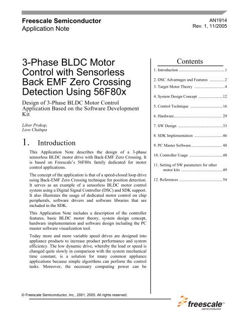
Figure 4-1. System Concept<br />
3-<strong>Phase</strong> <strong>BLDC</strong> <strong>Motor</strong> <strong>Control</strong>, Rev. 1<br />
Three-<strong>Phase</strong><br />
Inverter<br />
Commutation<br />
<strong>Control</strong><br />
PWM<br />
Generator<br />
<strong>with</strong><br />
Dead Time<br />
PWM<br />
Duty<br />
Cycle<br />
DSP56F80x<br />
<strong>Sensorless</strong> Drive Concept<br />
3-ph<br />
<strong>BLDC</strong><br />
<strong>Motor</strong><br />
The <strong>Back</strong>-<strong>EMF</strong> zero crossing detection enables position recognition. The resistor network is used to divide<br />
sensed voltages down to a 0-3.3V voltage level. Zero Crossing detection is synchronized <strong>with</strong> the center of<br />
center aligned PWM signal by the SW in order to filter high voltage spikes produced by the switching of the<br />
IGBTs (MOSFETs). This signal is transferred to the device’s Encoder Input which is also used as a digital<br />
filter. The SW selects one of the phase comparator outputs which corresponds to the current commutation step.<br />
<strong>Freescale</strong> Semiconductor 15<br />
Preliminary
<strong>Control</strong> Technique<br />
5. <strong>Control</strong> Technique<br />
5.1 <strong>Control</strong> Technique - General Overview<br />
The general overview of used control technique is shown in Figure 4-1. It will be described in following<br />
subsections:<br />
• PWM voltage generation for <strong>BLDC</strong><br />
• <strong>Sensorless</strong> Commutation <strong>Control</strong><br />
• Speed <strong>Control</strong><br />
The implementation of the control technique <strong>with</strong> all the SW processes is shown in Flow Chart, State diagrams<br />
and Data Flow (see Figure 7-2 through Figure 7-8).<br />
5.2 PWM voltage Generation for <strong>BLDC</strong><br />
As was already explained, the three phase voltage system shown in Figure 3-2 needs to be created to run the<br />
<strong>BLDC</strong> motor. It is provided by 3-phase power stage <strong>with</strong> 6 IGBTs (MOSFET) controlled by the on-chip PWM<br />
module (see Figure 5-1). The PWM signals <strong>with</strong> state currents are shown in Figure 5-2 and Figure 5-3.<br />
Figure 5-2 shows that both Bottom and Top power switches of the “free“ phase must be switched off. This is<br />
needed for any effective control of Brushless DC motor <strong>with</strong> trapezoidal B<strong>EMF</strong>.<br />
POWER<br />
SOURCE<br />
DC VOLTAGE<br />
3-PHASE POWER STAGE<br />
PWM1<br />
S AT<br />
PWM2<br />
S AB<br />
PWM3<br />
S BT<br />
PWM4<br />
S BT<br />
MOSFET/IGBT DRIVERS<br />
3-<strong>Phase</strong> <strong>BLDC</strong> <strong>Motor</strong> <strong>Control</strong>, Rev. 1<br />
3-PHASE <strong>BLDC</strong> MOT<br />
16 <strong>Freescale</strong> Semiconductor<br />
Preliminary<br />
PWM5<br />
S CT<br />
PWM6<br />
S CT<br />
PWM1 PWM2 PWM3 PWM4 PWM5 PWM6<br />
PULSE WIDTH MODULATOR<br />
(PWM) MODULE<br />
A<br />
56F80X<br />
Figure 5-1. PWM <strong>with</strong> <strong>BLDC</strong> Power Stage<br />
B<br />
C
PWM1 S At<br />
PWM2 S Ab<br />
PWM3 S Bt<br />
PWM4 S Bb<br />
PWM5 S Ct<br />
PWM6 S Cb<br />
I A<br />
I B<br />
I C<br />
PWM1 S At<br />
PWM2 S Ab<br />
PWM3 S Bt<br />
PWM4 S Bb<br />
PWM5 S Ct<br />
PWM6 S Cb<br />
I A<br />
I B<br />
I C<br />
A-off<br />
A-off<br />
A-off<br />
commutation commutation commutation commutation<br />
commutation commutation commutation<br />
B-off<br />
B-off<br />
A-off<br />
A-off<br />
C-off C-off<br />
C-off<br />
C-off<br />
B-off<br />
A-off<br />
C-off<br />
C-off<br />
B-off<br />
B-off<br />
B-off<br />
A-off<br />
A-off<br />
A-off<br />
0 60 120 180 240 300 360<br />
3-<strong>Phase</strong> <strong>BLDC</strong> <strong>Motor</strong> <strong>Control</strong>, Rev. 1<br />
C-off<br />
C-off<br />
C-off<br />
Figure 5-2. 3-phase <strong>BLDC</strong> <strong>Motor</strong> Commutation PWM Signal<br />
Commutation Commutation<br />
60 120<br />
Figure 5-3. <strong>BLDC</strong> Commutation <strong>with</strong> Bipolar (Hard) Switching<br />
PWM voltage Generation for <strong>BLDC</strong><br />
electrical angle<br />
electrical angle<br />
<strong>Freescale</strong> Semiconductor 17<br />
Preliminary
<strong>Control</strong> Technique<br />
Figure 5-3 shows that the diagonal power switches are driven by the same PWM signal as shown <strong>with</strong> arrow<br />
lines. This technique is called bipolar (hard) switching. The voltage across the two connected coils is always<br />
±DC bus voltage whenever there is a current flowing through these coils. Thus the condition for successful<br />
B<strong>EMF</strong> Zero Crossing sensing is fulfilled as described in Section 3.<br />
5.3 B<strong>EMF</strong> Zero Crossing Sensing<br />
5.3.1 B<strong>EMF</strong> Zero Crossing Checking<br />
The B<strong>EMF</strong> Zero Crossing of the 3 phases is checked using hardware comparators as described in Section 3.<br />
The outputs of the comparators are led to Quadrature Decoder Inputs. Where the digital filtration block is used<br />
to filter the spike on the Zero Crossing signals.<br />
The software selects the “free” phase at each commutation step and reads the filtered signal to detect the<br />
B<strong>EMF</strong> Zero Crossing event.<br />
5.3.2 B<strong>EMF</strong> Zero Crossing Synchronization <strong>with</strong> PWM<br />
The power stage PWM switching causes the high voltage transient of the phase voltages. This transient is<br />
passed to “free” phase due to mutual capacitor between the motor windings coupling. Figure 5-4 shows that<br />
free phase “branch” voltage U va is disturbed by PWM voltage shown on phase “branch” voltage U vb .<br />
Figure 5-4. B<strong>EMF</strong> Zero Crossing Synchronization <strong>with</strong> PWM<br />
3-<strong>Phase</strong> <strong>BLDC</strong> <strong>Motor</strong> <strong>Control</strong>, Rev. 1<br />
18 <strong>Freescale</strong> Semiconductor<br />
Preliminary<br />
u va<br />
u vb<br />
Zero Crossing Sample<br />
s/w flag<br />
The non-fed phase “branch” voltage U va is disturbed at the PWM edges. Therefore the presented <strong>BLDC</strong> <strong>Motor</strong><br />
<strong>Control</strong> application synchronizes the B<strong>EMF</strong> Zero Crossing detection <strong>with</strong> PWM.<br />
5.4 <strong>Sensorless</strong> Commutation <strong>Control</strong><br />
This chapter concentrates on sensorless <strong>BLDC</strong> motor commutation <strong>with</strong> B<strong>EMF</strong> Zero Crossing technique.<br />
In order to start and run the <strong>BLDC</strong> motor, the control algorithm has to go through the following states:<br />
• Alignment<br />
• Starting (<strong>Back</strong>-<strong>EMF</strong> Acquisition)<br />
• Running
3-<strong>Phase</strong> <strong>BLDC</strong> <strong>Motor</strong> <strong>Control</strong>, Rev. 1<br />
<strong>Sensorless</strong> Commutation <strong>Control</strong><br />
Figure 5-5 shows the transitions between the states. First the rotor is aligned to a known position; then the<br />
rotation is started <strong>with</strong>out the position feedback. When the rotor moves, the <strong>Back</strong>-<strong>EMF</strong> is acquired so the<br />
position is known and can be used to calculate the speed and processing of the commutation in the Running<br />
state.<br />
5.4.1 Alignment<br />
Start motor<br />
Alignment<br />
Alignment time<br />
expired?<br />
Yes<br />
Starting<br />
(B<strong>EMF</strong> Acquisition)<br />
Minimal correct<br />
commutations done?<br />
Yes<br />
Running<br />
<strong>Freescale</strong> Semiconductor 19<br />
Preliminary<br />
No<br />
No<br />
Figure 5-5. Commutation <strong>Control</strong> Stages<br />
Before the motor starts, there is a short time (which depends on the motor’s electrical time constant) when the<br />
rotor position is stabilized by applying PWM signals to only two motor phases (no commutation). The Current<br />
<strong>Control</strong>ler keeps the current <strong>with</strong>in predefined limits. This state is necessary in order to create a high start-up<br />
torque. When the preset time-out expires then this state is finished.<br />
• The Current <strong>Control</strong>ler subroutine <strong>with</strong> PI regulator is called to control DC Bus current. It sets the<br />
correct PWM ratio for the required current.<br />
The current PI controller works <strong>with</strong> constant execution (sampling) period determined by PWM frequency:<br />
Current <strong>Control</strong>ler period = 1/PWM frequency.
<strong>Control</strong> Technique<br />
The <strong>BLDC</strong> motor rotor position <strong>with</strong> flux vectors during alignment is shown in Figure 5-6.<br />
5.4.2 Running<br />
Figure 5-6. Alignment<br />
The commutation process is the series of states which assure that the <strong>Back</strong>-<strong>EMF</strong> zero crossing is successfully<br />
captured, the new commutation time is calculated and, finally, the commutation is performed. The following<br />
processes needs to be provided:<br />
• <strong>BLDC</strong> motor commutation service<br />
• <strong>Back</strong>-<strong>EMF</strong> Zero Crossing moment capture service<br />
• Computation of commutation times<br />
• Handler for interaction between these commutation processes<br />
5.4.2.1 Algorithms <strong>BLDC</strong> <strong>Motor</strong> Commutation <strong>with</strong> Zero Crossing Sensing<br />
All these processes are provided by new algorithms which were designed for these type of applications <strong>with</strong>in<br />
SDK. They are described in <strong>Motor</strong> <strong>Control</strong>.pdf, chapter <strong>BLDC</strong> <strong>Motor</strong> Commutation <strong>with</strong> Zero Crossing<br />
Sensing (see [12.1]).<br />
From pictures an overview of how the commutation works can be understood. After commuting the motor<br />
phases there is a time interval (Per_Toff[n]) when the shape of <strong>Back</strong>-<strong>EMF</strong> must stabilized (after the<br />
commutation the fly-back diodes are conducting the decaying phase current, therefore sensing of the<br />
<strong>Back</strong>-<strong>EMF</strong> is not possible). Then the new commutation time (T2[n]) is preset. The new commutation will be<br />
performed at this time if the <strong>Back</strong>-<strong>EMF</strong> zero crossing is not captured. If the <strong>Back</strong>-<strong>EMF</strong> zero crossing is<br />
3-<strong>Phase</strong> <strong>BLDC</strong> <strong>Motor</strong> <strong>Control</strong>, Rev. 1<br />
20 <strong>Freescale</strong> Semiconductor<br />
Preliminary
3-<strong>Phase</strong> <strong>BLDC</strong> <strong>Motor</strong> <strong>Control</strong>, Rev. 1<br />
<strong>Sensorless</strong> Commutation <strong>Control</strong><br />
captured before the preset commutation time expires, then the exact calculation of the commutation time<br />
(T2*[n]) is made based on the captured zero crossing time (T_ZCros[n]). The new commutation is performed<br />
at this new time.<br />
If (for any reason) the <strong>Back</strong>-<strong>EMF</strong> feedback is lost <strong>with</strong>in one commutation period corrective actions are taken<br />
in order to return to the regular states.<br />
The flow chart explaining the principle of <strong>BLDC</strong> Commutation<strong>Control</strong> <strong>with</strong> B<strong>EMF</strong> Zero Crossing Sensing is<br />
shown in Figure 5-7.<br />
<strong>Freescale</strong> Semiconductor 21<br />
Preliminary
<strong>Control</strong> Technique<br />
No<br />
Commutation Done<br />
B<strong>EMF</strong> Zero Crossing<br />
detected between previous<br />
commutations?<br />
Yes<br />
Service of Commutation:<br />
Preset commutation<br />
Wait for Per_Toff until phase<br />
current decays to zero<br />
B<strong>EMF</strong> Zero Crossing<br />
missed?<br />
No<br />
B<strong>EMF</strong> Zero Crossing<br />
Detected?<br />
No<br />
has commutation<br />
time expired?<br />
Yes<br />
Yes<br />
No<br />
Yes<br />
Make <strong>Motor</strong> Commutation<br />
Corrective Calculation 1.<br />
B<strong>EMF</strong> Zero Crossing missed<br />
Corrective Calculation 2.<br />
corrected setting of<br />
commutation time<br />
Service of received B<strong>EMF</strong><br />
Zero Crossing:<br />
corrected setting of<br />
commutation time<br />
Yes<br />
has commutation<br />
time expired?<br />
Figure 5-7. Flow Chart - <strong>BLDC</strong> Commutation <strong>with</strong> B<strong>EMF</strong> Zero Crossing Sensing<br />
3-<strong>Phase</strong> <strong>BLDC</strong> <strong>Motor</strong> <strong>Control</strong>, Rev. 1<br />
22 <strong>Freescale</strong> Semiconductor<br />
Preliminary<br />
No
5.4.2.2 Running - Commutation Times Calculation<br />
3-<strong>Phase</strong> <strong>BLDC</strong> <strong>Motor</strong> <strong>Control</strong>, Rev. 1<br />
<strong>Sensorless</strong> Commutation <strong>Control</strong><br />
Commutation time calculation is provided by algorithm bldcZCComput described in <strong>Motor</strong> <strong>Control</strong>.pdf,<br />
chapter <strong>BLDC</strong> <strong>Motor</strong> Commutation <strong>with</strong> Zero Crossing Sensing (see [12.1]).<br />
T_Cmt0[n-2] T_Cmt0[n-1] T_Cmt0[n]<br />
Per_ZCros[n-2]<br />
n-2 n-1 n<br />
Zero Crossing<br />
Detection Signal<br />
Per_ZCros0[n] =<br />
Per_ZCros[n-1]<br />
Zero Crossing<br />
Detection Signal<br />
T_ZCros[n-1]<br />
Per_Toff[n]<br />
Zero Crossing<br />
Detection Signal<br />
COEF_CMT_PRESET *<br />
* Per_ZCrosFlt[n-1]<br />
Per_ZCros[n]<br />
Per_ZCros[n]<br />
Per_ZCros[n]<br />
Per_HlfCmt[n]<br />
T_ZCros[n]<br />
Per_HlfCmt[n]<br />
T_Next[n]<br />
Commutation is preset<br />
T_Cmt0**[n+1]<br />
Commuted at preset time.<br />
No <strong>Back</strong>-<strong>EMF</strong> feedback<br />
was received<br />
- Corrective Calculation 1.<br />
T_Cmt0*[n+1]<br />
<strong>Back</strong>-<strong>EMF</strong> feedback<br />
received and evaluated<br />
Commuted when <strong>Back</strong>-<strong>EMF</strong><br />
Zero Crossing is missed<br />
- Corrective Calculation 2.<br />
Figure 5-8. <strong>BLDC</strong> Commutation Times <strong>with</strong> Zero Crossing sensing<br />
The following calculations are made to calculate the commutation times (T_Next[n])<br />
during the Running Stage:<br />
• Service of Commutation - The commutation time (T_Next[n]) is predicted:<br />
T_Next[n] = T_Cmt0[n] + Per_CmtPreset[n] =<br />
= T_Cmt0[n] + Coef_CmtPrecomp*Per_ZCrosFlt[n-1]<br />
coefficient Coef_CmtPrecomp = 2 at Running Stage!<br />
If Coef_CmtPrecomp*Per_ZCrosFlt>Max_PerCmt<br />
then result is limited at Max_PerCmt<br />
<strong>Freescale</strong> Semiconductor 23<br />
Preliminary
<strong>Control</strong> Technique<br />
• Service of received <strong>Back</strong>-<strong>EMF</strong> zero crossing - The commutation time (T_Next*[n]) is evaluated<br />
from the captured <strong>Back</strong>-<strong>EMF</strong> zero crossing time (T_ZCros[n]):<br />
Per_ZCros[n] = T_ZCros[n] - T_ZCros[n-1] = T_ZCros[n] - T_ZCros0<br />
Per_ZCrosFlt[n] = (1/2*Per_ZCros[n]+1/2*Per_ZCros0)<br />
HlfCmt[n] = 1/2*Per_ZCrosFlt[n]- Advance_angle =<br />
= 1/2*Per_ZCrosFlt[n]- C_CMT_ADVANCE*Per_ZCrosFlt[n]=<br />
Coef_HlfCmt*Per_ZCrosFlt[n]<br />
The best commutation was get <strong>with</strong> Advance_angle: 60Deg*1/8 = 7.5Deg<br />
which means Coef_HlfCmt = 0.375 at Running Stage!<br />
Per_Toff[n+1] = Per_ZCrosFlt*Coef_Toff and Max_PerCmtProc minimum<br />
Coef_Toff = 0.35 at Running Stage, Max_PerCmtProc = 100!<br />
Per_ZCros0
3-<strong>Phase</strong> <strong>BLDC</strong> <strong>Motor</strong> <strong>Control</strong>, Rev. 1<br />
<strong>Sensorless</strong> Commutation <strong>Control</strong><br />
• Where:<br />
T_Cnt0 = time of the last commutation<br />
T_Next = Time of the Next Time event (for Timer Setting)<br />
T_zCros = Time of the last Zero Crossing<br />
T_zCros0 = Time of the previous Zero Crossing<br />
Per_Toff = Period of the Zero Crossing off<br />
Per_CmtPreset = Preset Commutation Periof from commutation to next commutation if no<br />
Zero Crossing was captured<br />
Per_ZCros = Period between Zero Crossings (estimates required commutation period)<br />
Per_ZCros0 = Pervious period between Zero Crossings<br />
Per_ZCrosFlt = Estimated period of commutation filtered<br />
Per_HlfCmt = Period from Zero Crossing to commutation (half commutation)<br />
The required commutation timing is provided by setting of commutation constants Coef_CmtPrecompFrac,<br />
Coef_CmtPrecompLShft, Coef_HlfCmt, Coef_Toff, in structure RunComputInit.<br />
5.4.3 Starting (<strong>Back</strong>-<strong>EMF</strong> Acquisition)<br />
The <strong>Back</strong>-<strong>EMF</strong> sensing technique enables a sensorless detection of the rotor position, however the drive must<br />
be first started <strong>with</strong>out this feedback. It is caused by the fact that the amplitude of the induced voltage is<br />
proportional to the motor speed. Hence, the <strong>Back</strong>-<strong>EMF</strong> cannot be sensed at a very low speed and a special<br />
start-up algorithm must be performed.<br />
In order to start the <strong>BLDC</strong> motor the adequate torque must be generated. The motor torque is proportional to<br />
the multiplication of the stator magnetic flux, the rotor magnetic flux and the sine of angle between these<br />
magnetic fluxes.<br />
It implies (for <strong>BLDC</strong> motors) the following:<br />
1. The level of phase current must be high enough.<br />
2. The angle between the stator and rotor magnetic fields must be 90deg±30deg.<br />
The first condition is satisfied during the Alignment state by keeping the DC Bus current on the level which is<br />
sufficient to start the motor. In the Starting (<strong>Back</strong>-<strong>EMF</strong> Acquisition) state the same value of PWM duty cycle<br />
is used as the one which has stabilized the DC-Bus current during the Align state.<br />
The second condition is more difficult to fulfill <strong>with</strong>out any position feedback information. After the<br />
Alignment state the stator and the rotor magnetic fields are aligned (0deg angle). Therefore the two fast (faster<br />
then the rotor can follow) commutations must be applied to create an angular difference of the magnetic fields<br />
(see Figure 5-9).<br />
The commutation time is defined by start commutation period (Per_CmtStart).<br />
This allows starting the motor such that minimal speed (defined by state when <strong>Back</strong>-<strong>EMF</strong> can be sensed) is<br />
achieved during several commutations while producing the required torque. Until the <strong>Back</strong>-<strong>EMF</strong> feedback is<br />
locked the Commutation Process (explained in Section 5.4.2) assures that commutations are done in advance,<br />
so that successive <strong>Back</strong>-<strong>EMF</strong> zero crossing events are not missed.<br />
After several successive <strong>Back</strong>-<strong>EMF</strong> zero crossings the exact commutation times can be calculated. The<br />
commutation process is adjusted and the control flow continues to the Running state. The <strong>BLDC</strong> motor is then<br />
running <strong>with</strong> regular feedback and the speed controller can be used to control the motor speed by changing the<br />
PWM duty cycle value.<br />
<strong>Freescale</strong> Semiconductor 25<br />
Preliminary
<strong>Control</strong> Technique<br />
at steady-state condition<br />
<strong>with</strong> regular <strong>Back</strong>-<strong>EMF</strong> feedback<br />
Stator magnetic field Rotor magnetic<br />
field<br />
(created by PM)<br />
Border of<br />
stator pole<br />
Rotor movement<br />
during one<br />
commutation<br />
Zero crossing<br />
edge indicator<br />
<strong>Motor</strong> is Running<br />
Direction of<br />
<strong>Phase</strong> current<br />
<strong>Phase</strong> winding<br />
<strong>Motor</strong> is Starting<br />
Alignment Stage<br />
The rotor position is stabilized by<br />
applying PWM signals to only two<br />
motor phases<br />
Starting (B<strong>EMF</strong> Acquisition)<br />
The two fast (faster then the rotor can<br />
move) commutations are applied to<br />
create an angular difference of the<br />
stator magnetic field and rotor<br />
magnetic field.<br />
The <strong>Back</strong>-<strong>EMF</strong> feedback is tested.<br />
When the <strong>Back</strong>-<strong>EMF</strong> zero crossing<br />
is recognized the time of new<br />
commutation is evaluated. Until at<br />
least two successive <strong>Back</strong>-<strong>EMF</strong> zero<br />
crossings are received the exact<br />
commutation time can not be<br />
calculated. Therefore the<br />
commutation is done in advance in<br />
order to assure that successive<br />
<strong>Back</strong>-<strong>EMF</strong> zero crossing events<br />
would not be missed.<br />
Running<br />
Figure 5-9. Vectors of Magnetic Fields<br />
3-<strong>Phase</strong> <strong>BLDC</strong> <strong>Motor</strong> <strong>Control</strong>, Rev. 1<br />
After several <strong>Back</strong>-<strong>EMF</strong> zero<br />
crossing events the exact<br />
commutation time is calculated. The<br />
commutation process is adjusted.<br />
<strong>Motor</strong> is running <strong>with</strong> regular<br />
<strong>Back</strong>-<strong>EMF</strong> feedback.<br />
26 <strong>Freescale</strong> Semiconductor<br />
Preliminary
<strong>Phase</strong> <strong>Back</strong>-<strong>EMF</strong>s<br />
<strong>Back</strong>-<strong>EMF</strong> Zero Crossings<br />
Ideal Commutation Pattern when position is known<br />
B TOP<br />
C BOT<br />
Real Commutation Pattern when position is estimated<br />
B TOP<br />
C BOT<br />
Align<br />
<strong>Phase</strong> C<br />
<strong>Phase</strong> B<br />
<strong>Phase</strong> A<br />
CTOP ATOP BTOP CTOP ABOT BBOT CBOT ABOT CTOP ATOP BTOP CTOP ABOT BBOT CBOT ABOT 1’ st 2’ nd 3’ rd 4’ rd .................<br />
Starting (<strong>Back</strong>-<strong>EMF</strong> Acquisition)<br />
Figure 5-10. <strong>Back</strong>-<strong>EMF</strong> at Start-Up<br />
3-<strong>Phase</strong> <strong>BLDC</strong> <strong>Motor</strong> <strong>Control</strong>, Rev. 1<br />
<strong>Sensorless</strong> Commutation <strong>Control</strong><br />
Running<br />
Figure 5-10 demonstrates the <strong>Back</strong>-<strong>EMF</strong> during the start-up. The amplitude of the <strong>Back</strong>-<strong>EMF</strong> varies<br />
according to the rotor speed. During the Starting (<strong>Back</strong>-<strong>EMF</strong> Acquisition) state the commutation is done in<br />
advance. In the Running state the commutation is done at the right moments.<br />
Figure 5-11 illustrates the sequence of the commutations during the Starting (<strong>Back</strong>-<strong>EMF</strong> Acquisition) Stage.<br />
The commutation times T2[1] and T2[2] are calculated <strong>with</strong>out any influence of <strong>Back</strong>-<strong>EMF</strong> feedback.<br />
<strong>Freescale</strong> Semiconductor 27<br />
Preliminary
<strong>Control</strong> Technique<br />
.<br />
T_Cmt0[1] T_Cmt0[2] T_Cmt0[3]<br />
Per_CmtStart 2*Per_CmtStart<br />
T_ZCros[0]<br />
T2[1] T2[2] T2[n]<br />
n=1 n=2 n=3<br />
Zero Crossing<br />
Detection Signal<br />
Zero Crossing<br />
Detection Signal<br />
Zero Crossing<br />
Detection Signal<br />
Per_Toff[n]<br />
COEF_CMT_PRESET *<br />
* Per_ZCrosFlt[n-1]<br />
Per_HlfCmt[n]<br />
T_ZCros[n]<br />
T2**[n]<br />
Per_HlfCmt[n]<br />
T2*[n]<br />
3-<strong>Phase</strong> <strong>BLDC</strong> <strong>Motor</strong> <strong>Control</strong>, Rev. 1<br />
Commutation is preset<br />
Commuted at preset time.<br />
No <strong>Back</strong>-<strong>EMF</strong> feedback was<br />
received - Corrective Calculation 1.<br />
Commuted when correct<br />
<strong>Back</strong>-<strong>EMF</strong> feedback<br />
received and evaluated.<br />
Commuted when <strong>Back</strong>-<strong>EMF</strong><br />
Zero Crossing is missed<br />
- Corrective Calculation 2.<br />
Figure 5-11. Calculation of the Commutation Times during the Starting (<strong>Back</strong>-<strong>EMF</strong> Acquisition)<br />
Stage<br />
5.4.3.1 Starting - Commutation Times Calculation<br />
The calculations made during Starting (<strong>Back</strong>-<strong>EMF</strong> Acquisition) Stage can be seen in <strong>Motor</strong> <strong>Control</strong>.pdf,<br />
chapter <strong>BLDC</strong> <strong>Motor</strong> Commutation <strong>with</strong> Zero Crossing Sensing (see Section 12.2).<br />
Even the sub-states of the commutation process of Starting (<strong>Back</strong>-<strong>EMF</strong> Acquisition) state remain the same as<br />
during Running state, the required commutation timing depends on MCS state (Starting Stage, Running Stage).<br />
It is provided by different setting of commutation constants Coef_CmtPrecompFrac,<br />
Coef_CmtPrecompLShft, Coef_HlfCmt, Coef_Toff, in structure StartComputInit (differs from<br />
RunComputInit). So the commutation times calculation is same as described in Section 5.4.2.2, but the<br />
following computation coefficients are different:<br />
coefficient Coef_CmtPrecomp = 2 at Starting Stage!<br />
coefficient Coef_HlfCmt = 0.125 <strong>with</strong> advanced angle Advance_angle: 60Deg*3/8 = 22.5Deg<br />
at Starting Stage!<br />
Coef_Toff = 0.5 at Running Stage, Max_PerCmtProc = 100!<br />
28 <strong>Freescale</strong> Semiconductor<br />
Preliminary
3-<strong>Phase</strong> <strong>BLDC</strong> <strong>Motor</strong> <strong>Control</strong>, Rev. 1<br />
System Outline<br />
5.5 Speed <strong>Control</strong><br />
The speed close loop control is provided by a well known PI regulator as shown in Section 7.2.4. The actual<br />
speed (Omega_Actual) is computed from average of two B<strong>EMF</strong> Zero Crossing periods (time intervals)<br />
received from the sensorless commutation control block.<br />
The speed controller works <strong>with</strong> constant execution (sampling) period PER_SPEED_SAMPLE_S (request<br />
from timer interrupt).<br />
6. Hardware<br />
6.1 System Outline<br />
The motor control system is designed to drive the 3-phase <strong>BLDC</strong> motor in a speed closed loop.<br />
There are more software versions targeted for a specific device and Evaluation Module:<br />
• 56F803<br />
• 56F805<br />
• 56F807<br />
The hardware setup of the system for a particular device varies only by the EVM Board used. The application<br />
software is identical for all devices; the EVM and chip differences are handled by SDK drivers for the<br />
particular EVM board.<br />
Automatic board identification allows one software program runs on each of three hardware and motor<br />
platforms <strong>with</strong>out any change of parameters:<br />
• Low Voltage Evaluation <strong>Motor</strong> Hardware Set<br />
• Low Voltage Hardware Set<br />
• High Voltage Hardware Set<br />
The hardware setup is shown in Figure 6-1, Figure 6-2 and Figure 6-3. More information can also be found in<br />
Section 12.1.<br />
Notes: The detailed description of individual boards can be found in comprehensive user’s manuals belonging<br />
to each board. The user’s manual incorporates the schematic of the board, description of individual<br />
function blocks and bill of materials. The individual boards can be ordered from <strong>Freescale</strong> as a<br />
standard product.<br />
<strong>Freescale</strong> Semiconductor 29<br />
Preliminary
Hardware<br />
6.2 Low Voltage Evaluation <strong>Motor</strong> Hardware Set<br />
The system configuration is shown in Figure 6-1.<br />
+12<br />
J3<br />
GND <strong>Motor</strong> Board J1<br />
12VDC<br />
M1<br />
U2<br />
Evaluation<br />
J2<br />
IB23810<br />
<strong>Motor</strong><br />
40w flat<br />
ribbon<br />
cable<br />
ECMTREVAL<br />
3-<strong>Phase</strong> <strong>BLDC</strong> <strong>Motor</strong> <strong>Control</strong>, Rev. 1<br />
<strong>Control</strong>ler Board<br />
DSP56805EVM<br />
(DSP56803EVM)<br />
30 <strong>Freescale</strong> Semiconductor<br />
Preliminary<br />
J30<br />
(P1)<br />
Figure 6-1. Low Voltage Evaluation <strong>Motor</strong> Hardware System Configuration<br />
All the system parts are supplied and documented according the following references:<br />
• M1 - IB23810 <strong>Motor</strong><br />
— supplied in kit <strong>with</strong> IB23810 <strong>Motor</strong> as: ECMTREVAL - Evaluation <strong>Motor</strong> Board Kit<br />
• U2 3 ph AC/<strong>BLDC</strong> Low Voltage POWER STAGE:<br />
— supplied in kit <strong>with</strong> IB23810 <strong>Motor</strong> as: ECMTREVAL - Evaluation <strong>Motor</strong> Board Kit<br />
— described in: Evaluation <strong>Motor</strong> Board User’s Manual<br />
• U1 CONTROLLER BOARD for 56F805:<br />
— supplied as: 56F805EVM<br />
— described in: 56F805 Evaluation Module Hardware User’s Manual<br />
• or U1 CONTROLLER BOARD for 56F803:<br />
— supplied as: 56F803EVM<br />
— described in: 56F803 Evaluation Module Hardware User’s Manual<br />
Information of all above mentioned boards and documents can be found on:<br />
http://mot-sps.com/motor/devtools/index.html<br />
U1
6.3 Low Voltage Hardware Set<br />
The system configuration is shown in Figure 6-2.<br />
+12<br />
GND<br />
12VDC<br />
U2<br />
J19<br />
J20<br />
MB1<br />
J16 J17 J18<br />
Black<br />
White<br />
Red<br />
3ph AC/<strong>BLDC</strong><br />
Low Voltage<br />
Power Stage<br />
SM40N<br />
ECLOVAC<strong>BLDC</strong><br />
J5<br />
Red<br />
White<br />
Black<br />
Not Connected Not Connected<br />
Figure 6-2. Low Voltage Hardware System Configuration<br />
3-<strong>Phase</strong> <strong>BLDC</strong> <strong>Motor</strong> <strong>Control</strong>, Rev. 1<br />
Low Voltage Hardware Set<br />
<strong>Freescale</strong> Semiconductor 31<br />
Preliminary<br />
J13<br />
<strong>Motor</strong>-Brake<br />
SG40N<br />
40w flat<br />
ribbon<br />
cable<br />
J30<br />
(P1)<br />
U1<br />
ECMTRLOV<strong>BLDC</strong><br />
All the system parts are supplied and documented according the following references:<br />
• U1 <strong>Control</strong>ler Board for 56F805:<br />
— supplied as: 56F805EVM<br />
— described in: 56F805 Evaluation Module Hardware User’s Manual<br />
• or U1 <strong>Control</strong>ler Board for 56F803:<br />
— supplied as: 56F803EVM<br />
— described in: 56F803 Evaluation Module Hardware User’s Manual<br />
• U2 - 3 ph AC/<strong>BLDC</strong> Low Voltage Power Stage<br />
— supplied as: ECLOVAC<strong>BLDC</strong><br />
— described in: 3 <strong>Phase</strong> Brushless DC Low Voltage Power Stage<br />
• MB1 - <strong>Motor</strong>-Brake SM40N + SG40N<br />
— supplied as: ECMTRLOV<strong>BLDC</strong><br />
Information of all above mentioned boards and documents can be found on:<br />
http://mot-sps.com/motor/devtools/index.html<br />
<strong>Control</strong>ler Board<br />
DSP56805EVM<br />
(DSP56803EVM)
Hardware<br />
6.4 High Voltage Hardware Set<br />
The system configuration is shown in Figure 6-3.<br />
L<br />
N<br />
PE<br />
100 - 240VAC<br />
49 - 61 Hz<br />
U2<br />
MB1<br />
J11.1<br />
J11.2<br />
Black<br />
White<br />
Red<br />
Not Connected<br />
3ph AC/<strong>BLDC</strong><br />
High Voltage<br />
+12VDC<br />
GND<br />
40w flat ribbon<br />
cable<br />
Power Stage J14<br />
J1 Board<br />
J2<br />
J30<br />
(P1)<br />
J13.1 J13.2 J13.3<br />
SM40V<br />
J5<br />
<strong>Motor</strong>-Brake<br />
SG40N<br />
Red<br />
White<br />
Black<br />
Not Connected<br />
ECMTRHIV<strong>BLDC</strong><br />
Optoisolation<br />
3-<strong>Phase</strong> <strong>BLDC</strong> <strong>Motor</strong> <strong>Control</strong>, Rev. 1<br />
40w flat ribbon<br />
cable<br />
32 <strong>Freescale</strong> Semiconductor<br />
Preliminary<br />
U3<br />
ECOPT<br />
ECOPTHIVAC<strong>BLDC</strong><br />
JP1.1 JP1.2<br />
Figure 6-3. High Voltage Hardware System Configuration<br />
All the system parts are supplied and documented according the following references:<br />
U1<br />
<strong>Control</strong>ler Board<br />
• U1 - <strong>Control</strong>ler Board for 56F805:<br />
— supplied as: 56F805EVM<br />
— described in: Evaluation Module Hardware User’s Manual<br />
• or U1 - <strong>Control</strong>ler Board for 56F803:<br />
— supplied as: 56F803EVM<br />
— described in: 56F803 Evaluation Module Hardware User’s Manual<br />
• U2 - 3 ph AC/<strong>BLDC</strong> High Voltage Power Stage<br />
— supplied in kit <strong>with</strong> Optoisolation Board as: ECOPTHIVAC<strong>BLDC</strong><br />
— described in: 3 <strong>Phase</strong> Brushless DC High Voltage Power Stage<br />
• U3 - Optoisolation Board<br />
— supplied <strong>with</strong> 3 ph AC/<strong>BLDC</strong> High Voltage Power Stage as: ECOPTHIVAC<strong>BLDC</strong><br />
— or supplied alone as: ECOPT - ECOPT optoisolation board<br />
— described in: Optoisolation Board User’s Manual<br />
DSP56805EVM<br />
(DSP56803EVM)<br />
Warning: It is strongly recommended to use opto-isolation (optocouplers and optoisolation amplifiers) during<br />
the development time to avoid any damage to the development equipment.<br />
• MB1 <strong>Motor</strong>-Brake SM40V + SG40N<br />
— supplied as: ECMTRHIV<strong>BLDC</strong><br />
Information for all boards and documents can be found at:<br />
www.freescale.com
7. SW Design<br />
3-<strong>Phase</strong> <strong>BLDC</strong> <strong>Motor</strong> <strong>Control</strong>, Rev. 1<br />
Main SW Flow Chart<br />
This section describes the design of the software blocks of the drive. The software will be described in terms<br />
of:<br />
• Main Software Flow Chart<br />
• Data Flow<br />
• State Diagram<br />
For more information of the used control technique see Section 5.<br />
7.1 Main SW Flow Chart<br />
The main software flow chart incorporates the Main routine entered from Reset, and interrupt states. The Main<br />
routine includes the initialization of the device and the main loop. It is shown in Figure 7-1 and Figure 7-2.<br />
The main loop incorporates Application State Machine - the highest SW level which precedes settings for other<br />
software levels, <strong>BLDC</strong> motor Commutation <strong>Control</strong>, Speed <strong>Control</strong>, Alignment Current <strong>Control</strong>, etc. The<br />
inputs of Application State Machine are Run/Stop Switch state, Required Speed Omega and Drive Fault Status.<br />
Required Mechanical Speed can be set from PC master software or manually <strong>with</strong> Up/Down buttons.<br />
Commutation <strong>Control</strong> proceeds <strong>BLDC</strong> motor commutation <strong>with</strong> the states described in Section 5 and<br />
Section 7.3.4.<br />
The Speed <strong>Control</strong> is detailed description is in sections Section 7.2.3 and Section 7.3.5. Alignment Current<br />
<strong>Control</strong> is described in Section 7.2.4 and Section 7.3.6.<br />
Run/Stop switch is checked to provide an input for Application State Machine (ApplicationMode Start or<br />
Stop).<br />
The interrupt subroutines provide commutation Timer services, ADC starting in the PWM reload interrupt,<br />
ADC service, ADC Zero Crossing checking, Limit analog values handling, overcurrent and overvoltage PWM<br />
fault handler.<br />
The Commutation Timer ISR is used for Commutation Timing and Commutation <strong>Control</strong> and Zero Crossing<br />
Checking proceeding.<br />
The Speed/Alignment Timer ISR is used for Speed regulator time base and for Alignment stage duration<br />
timing.<br />
The PWM Reload ISR is used to evaluate B<strong>EMF</strong> Zero Crossing, start ADC conversion and memorize Zero<br />
Crossing sampling time T_ZCSample.<br />
The ADC Complete ISR is used to read voltages, current and temperature samples from the ADC. It also sets<br />
Current control and when the Current <strong>Control</strong> setting is enabled.<br />
The other interrupts in Figure 7-2 are used for System Fault handling and setting of Required Mechanical<br />
Speed input for Application State Machine (ApplicationMode Start or Stop).<br />
<strong>Freescale</strong> Semiconductor 33<br />
Preliminary
SW Design<br />
Reset<br />
Initialize<br />
Application State Machine:<br />
precedes/sets requirements of:<br />
Drive Fault Status<br />
Application Mode<br />
Omega Required Mechanical<br />
<strong>Control</strong> Speed<br />
<strong>Control</strong> Alignment Current<br />
Commutation <strong>Control</strong><br />
proceed Status_Commutation:<br />
Running<br />
Starting<br />
Alignment<br />
Stopped<br />
Check Run/Stop Switch<br />
Interrupt<br />
ADC complete<br />
ADC complete ISR:<br />
read Temperature<br />
DC bus Voltage/Current<br />
set Current <strong>Control</strong> Rq<br />
RTI<br />
3-<strong>Phase</strong> <strong>BLDC</strong> <strong>Motor</strong> <strong>Control</strong>, Rev. 1<br />
Interrupt<br />
OC Cmt Timer<br />
Commutation Timer OC ISR:<br />
<strong>Motor</strong> Commutation Timing<br />
Commutate. <strong>Control</strong> Proceed<br />
Zero Crossing Setting<br />
RTI<br />
Interrupt<br />
OC Cmt2Timer<br />
Speed/Alignment Timer OC ISR:<br />
set Speed <strong>Control</strong> Request<br />
Alignment stage timing<br />
RTI<br />
Interrupt<br />
PWM A Reload<br />
PWM Reload ISR:<br />
start ADC<br />
memorize sampling time<br />
evaluate Zero Crossing<br />
34 <strong>Freescale</strong> Semiconductor<br />
Preliminary<br />
RTI<br />
Figure 7-1. Main Software Flow Chart - Part 1
Interrupt<br />
Up Button<br />
Up Button ISR:<br />
increment<br />
Omega Required Mechanical<br />
RTI<br />
Interrupt<br />
ADC Low Limit<br />
ADC Low Limit ISR:<br />
set Undervoltage Fault<br />
set Overheating Fault<br />
Interrupt<br />
PWM A Fault<br />
PWM Fault ISR:<br />
set Overcurrent Fault<br />
set Overvoltage Fault<br />
Emergency Stop<br />
Interrupt<br />
ADC High Limit<br />
ADC High Limit ISR:<br />
set Overvoltage Fault<br />
set Overcurrent Fault<br />
Emergency Stop Emergency Stop<br />
RTI<br />
RTI<br />
Figure 7-2. Main Software Flow Chart - Part 2<br />
3-<strong>Phase</strong> <strong>BLDC</strong> <strong>Motor</strong> <strong>Control</strong>, Rev. 1<br />
Interrupt<br />
Down Button<br />
Down Button ISR:<br />
decrement<br />
Omega Required Mechanical<br />
RTI<br />
RTI<br />
Data Flow<br />
7.2 Data Flow<br />
The control algorithm obtains values from the user interface and sensors, processes them and generates 3-phase<br />
PWM signals for motor control as can be seen on the data flow analysis shown in Figure 7-3.<br />
<strong>Freescale</strong> Semiconductor 35<br />
Preliminary
SW Design<br />
DC-Bus Current<br />
(A/D)<br />
I_Dc_Bus Omega_Required_Mech ApplicationMode<br />
Cmd_Application<br />
Process<br />
Current PI <strong>Control</strong>ler<br />
Manual Speed PC<br />
Setting Master<br />
U_Desired<br />
Process<br />
Application<br />
State Machine<br />
Omega_Desired_Mech<br />
Process<br />
Speed PI <strong>Control</strong>ler<br />
START/STOP<br />
Switch<br />
Omega_Actual_Mech<br />
Process<br />
PWM Generation<br />
Status_Commutation<br />
BldcMode<br />
Step_Cmt,<br />
Cmt_Drv_RqFlag<br />
PVAL0,PVAL1 PVAL2,PVAL3 PVAL4,PVAL5<br />
Figure 7-3. Data Flow - Part 1<br />
3-<strong>Phase</strong> <strong>BLDC</strong> <strong>Motor</strong> <strong>Control</strong>, Rev. 1<br />
B<strong>EMF</strong> Zero Crossing<br />
Comparators<br />
Process<br />
Commutation <strong>Control</strong><br />
36 <strong>Freescale</strong> Semiconductor<br />
Preliminary
Protection processes are shown in Figure 7-4 and described in the following sub-sections.<br />
DC-Bus Current<br />
(A/D)<br />
I_Dc_Bus<br />
Process<br />
Application<br />
State Machine<br />
Temperature<br />
(A/D)<br />
Temperature<br />
Process<br />
Fault <strong>Control</strong><br />
DriveFaultStatus<br />
DC-Bus Voltage<br />
(A/D)<br />
U_Dc_Bus<br />
3-<strong>Phase</strong> <strong>BLDC</strong> <strong>Motor</strong> <strong>Control</strong>, Rev. 1<br />
Process<br />
PWM Generation<br />
PWM Faults<br />
(OverVoltage/OverCurrent)<br />
PVAL0,PVAL1 PVAL2,PVAL3 PVAL4,PVAL5<br />
Figure 7-4. Data Flow - part2<br />
Data Flow<br />
7.2.1 Process Application State Machine<br />
This process controls the application subprocesses by status and command words as can be seen in Figure 7-3.<br />
Based on the status of the Status_Commutation (set by the Commutation <strong>Control</strong> process) the<br />
Cmd_Application Rq flags are set to request calculation of the Current PI <strong>Control</strong>ler (Alignment state) or<br />
Speed PI <strong>Control</strong>ler (Running state) and to control the angular speed setting (reflects the status of the<br />
START/STOP Switch and the Run/Stop commands).<br />
7.2.2 Process Commutation <strong>Control</strong><br />
This process controls sensorless <strong>BLDC</strong> motor commutations as explained in Section 5. Its outputs, Step_Cmt<br />
and Cmt_Drv_RqFlag, are used to set the PWM Generation process. The output Omega_Actual_Mech is<br />
used for the Speed <strong>Control</strong>ler process.<br />
7.2.3 Process Speed PI <strong>Control</strong>ler<br />
The general principle of the speed PI control loop is illustrated in Figure 7-5.<br />
<strong>Freescale</strong> Semiconductor 37<br />
Preliminary
SW Design<br />
.<br />
Reference<br />
Speed<br />
(Omega_Desired)<br />
-<br />
Speed<br />
Error<br />
PI<br />
<strong>Control</strong>ler<br />
Corrected<br />
Speed<br />
(U_Desired)<br />
Figure 7-5. Closed Loop <strong>Control</strong> System<br />
3-<strong>Phase</strong> <strong>BLDC</strong> <strong>Motor</strong> <strong>Control</strong>, Rev. 1<br />
<strong>Control</strong>led<br />
System<br />
Actual <strong>Motor</strong><br />
Speed<br />
(Omega_Actual)<br />
The speed closed loop control is characterized by the feedback of the actual motor speed. This information is<br />
compared <strong>with</strong> the reference set point and the error signal is generated. The magnitude and polarity of the error<br />
signal corresponds to the difference between the actual and desired speed. Based on the speed error, the PI<br />
controller generates the corrected motor voltage in order to compensate for the error.<br />
The speed controller works <strong>with</strong> a constant execution (sampling) period. The request is driven from the timer<br />
interrupt <strong>with</strong> the constant PER_SPEED_SAMPLE_S. The PI controller is proportional and integral<br />
constants were set experimentally.<br />
7.2.4 Process Current PI <strong>Control</strong>ler<br />
The process is similar to the Speed controller. The I_Dc_Bus current is controlled based on the<br />
U_Dc_Bus_Desired Reference current. The current controller is processed only during Alignment stage.<br />
The current controller works <strong>with</strong> a constant execution (sampling) period. determined by PWM frequency:<br />
Current <strong>Control</strong>ler period = 1/pwm frequency.<br />
The PI controller is proportional and integral constants were set experimentally.<br />
7.2.5 Process PWM Generation<br />
The Process PWM Generation creates:<br />
• the <strong>BLDC</strong> motor commutation pattern as described in Section 1.<br />
• required duty cycle<br />
7.2.6 Process Fault <strong>Control</strong><br />
The Process Fault <strong>Control</strong> is used for drive protection. It can be understood from Figure 7-4. The<br />
DriveFaultStatus is passed to the PWM Generation process and to the Application State Machine process in<br />
order to disable the PWMs and to control the application accordingly.<br />
7.3 State Diagram<br />
The state diagrams of the whole SW are described below.<br />
38 <strong>Freescale</strong> Semiconductor<br />
Preliminary
7.3.1 Main SW States - General Overview<br />
The SW can be split into following processes:<br />
• Process Application State Machine<br />
• Process Commutation <strong>Control</strong><br />
• Process Speed PI <strong>Control</strong>ler<br />
• Process Current PI <strong>Control</strong>ler<br />
• Process PWM Generation<br />
• Process PWM Generation<br />
3-<strong>Phase</strong> <strong>BLDC</strong> <strong>Motor</strong> <strong>Control</strong>, Rev. 1<br />
State Diagram<br />
as shown in Section 7.2. The general overview of the software states is in the State Diagram - Process<br />
Application State Machine, which is the highest level (only the process Fault <strong>Control</strong> is on the same level<br />
because of the motor emergency stop).<br />
The status of all the processes after reset is defined in Section 7.3.2.<br />
7.3.2 Initialize<br />
In Main SW initialization provides following actions:<br />
• CmdApplication = 0<br />
• DriveFaultStatus = NO_FAULT<br />
• PCB <strong>Motor</strong> Set Identification<br />
— boardId function is used to detect one of 3 possible hardware sets. According to used hardware<br />
one of three control constant sets are loaded (functions EVM_<strong>Motor</strong>_Settings,<br />
LV_<strong>Motor</strong>_Settings, HV_<strong>Motor</strong>_Settings)<br />
• ADC Initialization<br />
• Led diodes initialization<br />
• Switch (Start/Stop) initialization<br />
• Push Buttons (Speed up/down) initialization<br />
• Commutation control initialization<br />
• PWM initialization<br />
• PWM fault interrupts initialization<br />
• Zero Crossing inputs = Quadrature decoder filter initialization<br />
• Output Compare Timers initialization<br />
Notes: The EVM board can be connected to the power stage boards. In order to assure the right hardware is<br />
connected the board identification is performed. When inappropriate hardware is detected the<br />
DriveFaultStatus|=WRONG_HARDWARE is set, motor remains stopped!<br />
7.3.3 State Diagram - Process Application State Machine<br />
Process Application State Machine state diagram is displayed in Figure 7-6. Application State Machine<br />
controls the main application functionality.<br />
The application can be controlled:<br />
• manually<br />
• from PC master software<br />
<strong>Freescale</strong> Semiconductor 39<br />
Preliminary
SW Design<br />
In manual control, the application is controlled <strong>with</strong> Start/Stop switch and Up Down Push buttons to set<br />
Required Speed.<br />
In PC master software control mode the Start/Stop is controlled manually and the Required Speed is set via the<br />
PC master software.<br />
The motor is stopped whenever the absolute value of Required speed is lower then Minimal Speed or switch<br />
set to stop or if there is a system failure - Drive Fault (Emergency Stop) state is entered. All the SW processes<br />
are controlled according this Application State Machine status.<br />
Reset<br />
Drive Fault<br />
Up Button<br />
Increment<br />
Required Speed<br />
(Switch = Stop) || (abs (Required Speed) Minimal Speed)<br />
Drive Fault<br />
Emergency Stop<br />
Down Button<br />
Decrement<br />
Required Speed<br />
3-<strong>Phase</strong> <strong>BLDC</strong> <strong>Motor</strong> <strong>Control</strong>, Rev. 1<br />
PC Master Software<br />
Required Speed setting<br />
Set<br />
Required Speed<br />
Figure 7-6. State Diagram - Process Application State Machine<br />
7.3.4 State Diagram - Process Commutation <strong>Control</strong><br />
Drive Fault<br />
State Diagram of the process Commutation <strong>Control</strong> is shown in Figure 7-7. The Commutation <strong>Control</strong> process<br />
takes care of the sensorless <strong>BLDC</strong> motor commutation. The requirement to run the <strong>BLDC</strong> motor is determined<br />
by upper software level Application State Machine. When the Application State Machine is in <strong>BLDC</strong> Stop<br />
state, Commutation <strong>Control</strong> status is Stopped. If it is in <strong>BLDC</strong> Stop state, the Commutation <strong>Control</strong> goes<br />
through the states described in section Section 5. So there are the following possible states:<br />
• Alignment state<br />
— motor is powered <strong>with</strong> current through 2 phases - no commutations provided.<br />
40 <strong>Freescale</strong> Semiconductor<br />
Preliminary
• Starting (<strong>Back</strong>-<strong>EMF</strong> Acquisition) State<br />
3-<strong>Phase</strong> <strong>BLDC</strong> <strong>Motor</strong> <strong>Control</strong>, Rev. 1<br />
State Diagram<br />
— motor is started <strong>with</strong> making first 2 commutations, then it is running as at Running state using Start<br />
parameters for commutation calculation StartComputInit (so the commutation advance angle and<br />
the Per_Toff time are different)<br />
• Running state<br />
— motor is running <strong>with</strong> Run parameters for commutation calculation RunComputInit.<br />
• Stopped state<br />
— motor is stopped <strong>with</strong> no power going to motor phases.<br />
Drive starts by setting the Alignment stage where the Alignment commutation step is set and Alignment stage<br />
is timed. After the time-out the Starting stage is entered <strong>with</strong> initialization of B<strong>EMF</strong> Zero Crossing algorithms.<br />
After the required number of successive commutations <strong>with</strong> correct Zero Crossing are done, the Running stage<br />
is entered. If the number of commutations <strong>with</strong> wrong Zero Crossing exceeds a pre-determined Maximal<br />
number, the Running and Starting stages are exited to the Stop stage. The commutation control is determined<br />
by the variable StatusCommutation.<br />
Reset<br />
Stopped<br />
Set Stop<br />
exceeded Maximal<br />
Zero Crossing<br />
Error commutations<br />
<strong>BLDC</strong> Run<br />
<strong>BLDC</strong> Stop<br />
Running<br />
Set Alignment<br />
done<br />
Alignment<br />
Set Running<br />
Alignment Time-out<br />
Set Starting<br />
Starting<br />
Minimal commutations<br />
<strong>with</strong> Zero Crossing OK<br />
passed<br />
<strong>Freescale</strong> Semiconductor 41<br />
Preliminary<br />
done<br />
done<br />
Figure 7-7. State Diagram - Process Commutation <strong>Control</strong><br />
7.3.4.1 Commutation <strong>Control</strong> - Running State<br />
The State diagram of Commutation <strong>Control</strong> state Running is shown in Figure 7-7 and is explained in<br />
Section 5. The selection of the state after the motor commutation depends on the detection of the B<strong>EMF</strong> Zero<br />
Crossing during previous commutation period. If no B<strong>EMF</strong> Zero Crossing was detected, the commutation<br />
period is corrected using Corrective Calculation 1. Then the Next Commutation time and commutation
SW Design<br />
registers are preset. If Zero Crossing already happen during Per_Toff time period, the commutation period is<br />
corrected using Corrective Calculation 2. When the commutation time expires, then a new commutation is<br />
performed.<br />
No Zero Crossing<br />
detected during last<br />
commutation period<br />
Running - Begin<br />
Calculate Next Commutation<br />
after No Zero Crossing<br />
Corrective Calculation 1.<br />
Preset Next Commutation<br />
settings and timing<br />
Zero Crossing Missed<br />
during Per_Toff<br />
motor Commutation<br />
commutation time<br />
(T_Next) expired<br />
Zero Crossing<br />
Detected/Missed during last<br />
commutation period<br />
Zero Crossing Get<br />
3-<strong>Phase</strong> <strong>BLDC</strong> <strong>Motor</strong> <strong>Control</strong>, Rev. 1<br />
Calculate Next Commutation<br />
after Zero Crossing Get<br />
Calculate Next Commutation<br />
after Zero Crossing Missed<br />
Corrective Calculation 2.<br />
Figure 7-8. Substates - Running<br />
This state is almost wholly serviced by the <strong>BLDC</strong> Zero Crossing algorithms which are documented in <strong>Motor</strong><br />
<strong>Control</strong>.pdf, chapter <strong>BLDC</strong> <strong>Motor</strong> Commutation <strong>with</strong> Zero Crossing Sensing (see Section 12.1). First the<br />
bldczcHndlr is called <strong>with</strong> actual time from Cmt Timer Counter to control requests and commutation control<br />
registers. Other <strong>BLDC</strong> Zero Crossing algorithms are called, according to the request flags. The state services<br />
are located in main loop and in Cmt (commutation) Timer Interrupt.<br />
7.3.4.2 Commutation <strong>Control</strong> - Starting state<br />
The starting state is the Running state as described in Figure 7-8.<br />
42 <strong>Freescale</strong> Semiconductor<br />
Preliminary
7.3.4.3 Commutation <strong>Control</strong> - Set Running<br />
3-<strong>Phase</strong> <strong>BLDC</strong> <strong>Motor</strong> <strong>Control</strong>, Rev. 1<br />
State Diagram<br />
This state services the transition from Starting (<strong>Back</strong>-<strong>EMF</strong> Acquisition) state to Running state by the <strong>BLDC</strong><br />
Zero Crossing algorithms (see Section 12.1) according to the following actions:<br />
• T_Actual = Cmt Timer Counter<br />
• setting new commutation parameters and initialized commutation <strong>with</strong> bldczcHndlrInit algorithm<br />
• initialization of computation <strong>with</strong> bldczcComputInit algorithm<br />
7.3.4.4 Commutation <strong>Control</strong> - Set Starting<br />
This state is used to set the start of the motor commutation.<br />
The following actions are performed in this state:<br />
• Commutation initialized to start commutation step and required direction<br />
• 2 additional motor commutations are prepared (in order to create starting torque)<br />
• setting commutation parameters and commutation handler initialization by bldczcHndlrInit<br />
algorithm<br />
• first action from bldczcHndlrInit algorithm (for commutations algorithms) is timed by Output<br />
Compare Timer for Commutation timing control (OC Cmt)<br />
• PWM is set according the above prepared motor commutation steps<br />
• Zero Crossing is initialized by bldcZCrosInit<br />
• Zero Crossing computation is initialized by bldczcComputInit<br />
• Zero Crossing is Enabled<br />
7.3.4.5 Commutation <strong>Control</strong> - Set Stop<br />
In this state:<br />
• bldczcHndlrStop algorithm is called<br />
• PWM output pad is disabled in order to stop motor rotation and switch off the motor power supply<br />
7.3.4.6 Commutation <strong>Control</strong> - Set Alignment<br />
In this state <strong>BLDC</strong> motor is set to Alignment state, where voltage is put across 2 motor phases and current is<br />
controlled to be at required value. The following actions are provided in Set Alignment state:<br />
• PWM set according to Align_Step_Cmt variable status<br />
• current controller is initialized<br />
• PWM output is enabled<br />
• Alignment Time is timed by Output Compare Timer for Speed and Alignment<br />
<strong>Freescale</strong> Semiconductor 43<br />
Preliminary
SW Design<br />
7.3.5 State Diagram - Process Speed PI <strong>Control</strong>ler<br />
Commutation<br />
Running<br />
U_Desired =<br />
PI (Reference Speed - Actual <strong>Motor</strong> Speed)<br />
Speed <strong>Control</strong><br />
Request<br />
Commutation<br />
Stopped/Alignment/Starting<br />
Set Speed <strong>Control</strong><br />
Request<br />
3-<strong>Phase</strong> <strong>BLDC</strong> <strong>Motor</strong> <strong>Control</strong>, Rev. 1<br />
Speed <strong>Control</strong><br />
Disabled<br />
Speed <strong>Control</strong><br />
Timer Interrupt<br />
(PER_SPEED_SAMPLE)<br />
Figure 7-9. State Diagram - Process Speed PI <strong>Control</strong>ler<br />
Reset<br />
The Speed PI controller algorithm controllerPItype1 is described in the SDK documentation. The controller<br />
execution (sampling) period is PER_SPEED_SAMPLE, period of Speed <strong>Control</strong> Timer Interrupt.<br />
44 <strong>Freescale</strong> Semiconductor<br />
Preliminary
7.3.6 State Diagram - Process Current PI <strong>Control</strong>ler<br />
U_Desired =<br />
PI (Reference Current - Actual Current)<br />
Current <strong>Control</strong><br />
Request<br />
Start ADC<br />
Conversions<br />
Commutation Status<br />
Alignment<br />
Commutation<br />
Stopped/Starting/Running<br />
PWM Reload<br />
Interrupt<br />
(PWM period)<br />
3-<strong>Phase</strong> <strong>BLDC</strong> <strong>Motor</strong> <strong>Control</strong>, Rev. 1<br />
Current <strong>Control</strong><br />
Disabled<br />
ADC Conversion<br />
Complete Interrupt<br />
(PWM period)<br />
Set Current <strong>Control</strong><br />
Request<br />
Figure 7-10. State Diagram - Process Speed PI <strong>Control</strong>ler<br />
Reset<br />
State Diagram<br />
The Current PI controller algorithm controllerPItype1 is described in the SDK documentation. The controller<br />
execution (sampling) period is determined by the PWM module period, because the ADC conversion is started<br />
each PWM reload (once per PWM period). The Current <strong>Control</strong> Request is set in ADC Conversion Complete<br />
Interrupt.<br />
7.3.7 State Diagram - Process Fault <strong>Control</strong><br />
The process Fault State is described by Interrupt subroutines which provide its functionality.<br />
7.3.7.1 PWM Fault A Interrupt Subroutine<br />
This subroutine is called at PWM A (or PWM in case of a 56F803) Fault Interrupt.<br />
In this interrupt subroutine following faults from PWM Fault pins are processed:<br />
• when Overvoltage occurs (the Overvoltage fault pin set)<br />
— DriveFaultStatus |= OVERVOLTAGE<br />
• when Overcurrent occurs (the Overcurrent fault pin set)<br />
— DriveFaultStatus |= OVERCURRENT<br />
<strong>Freescale</strong> Semiconductor 45<br />
Preliminary
SDK Implementation<br />
7.3.7.2 ADC Low Limit Interrupt Subroutine<br />
This subroutine is called when at least one ADC low limit is detected.<br />
In this interrupt subroutine following low limit exceeds are processed:<br />
• the undervoltage of the DC Bus voltage<br />
— DriveFaultStatus |= UNDERVOLTAGE_ADC_DCB<br />
• the over temperature (detected here because of the sensor reverse temperature characteristic)<br />
— DriveFaultStatus |= OVERHEATING<br />
7.3.7.3 ADC High Limit Interrupt Subroutine<br />
This subroutine is called when at least one ADC high limit is exceeded.<br />
In this interrupt subroutine following high limit exceeds are processed:<br />
• the overvoltage of the DC Bus voltage<br />
— DriveFaultStatus |= OVERVOLTAGE_ADC_DCB<br />
• the overcurrent of the DC bus current input<br />
— DriveFaultStatus |= OVERCURRENT_ADC_DCB<br />
8. SDK Implementation<br />
The Embedded SDK is a collection of APIs, libraries, services, rules and guidelines. This software<br />
infrastructure is designed to let 56F8xx software developers create high-level, efficient, portable code. This<br />
chapter describes how the <strong>BLDC</strong> motor control application <strong>with</strong> B<strong>EMF</strong> Zero Crossing is written under SDK.<br />
8.1 Drivers and Library Function<br />
The <strong>BLDC</strong> motor control application <strong>with</strong> B<strong>EMF</strong> Zero Crossing uses the following drivers:<br />
• ADC driver<br />
• Quadrature Timer driver<br />
• Quadrature encoder<br />
• PWM driver<br />
• Led driver<br />
• Switch driver<br />
• Button driver<br />
The all driver except Timer driver are included in BSP.LIB library. The Timer driver is included in SYS.LIB<br />
library.<br />
The <strong>BLDC</strong> motor control application <strong>with</strong> B<strong>EMF</strong> Zero Crossing uses the following library functions:<br />
• bldczcHndlrInit (handler initialization for <strong>BLDC</strong> commutation control <strong>with</strong> B<strong>EMF</strong> Zero Crossing;<br />
bldc.lib library)<br />
• bldczcHndlr (handler for <strong>BLDC</strong> commutation control <strong>with</strong> B<strong>EMF</strong> Zero Crossing; bldc.lib library)<br />
• bldczcTimeoutIntAlg (time-out interrupt algorithm for <strong>BLDC</strong> commutation control <strong>with</strong> B<strong>EMF</strong> Zero<br />
Crossing; bldc.lib library)<br />
3-<strong>Phase</strong> <strong>BLDC</strong> <strong>Motor</strong> <strong>Control</strong>, Rev. 1<br />
46 <strong>Freescale</strong> Semiconductor<br />
Preliminary
3-<strong>Phase</strong> <strong>BLDC</strong> <strong>Motor</strong> <strong>Control</strong>, Rev. 1<br />
Driver Initialization<br />
• bldczcHndlrStop (stop handler for <strong>BLDC</strong> commutation control <strong>with</strong> B<strong>EMF</strong> Zero Crossing; <strong>BLDC</strong>.LIB<br />
library)<br />
• bldczcComputInit (computation initialization for <strong>BLDC</strong> commutation control <strong>with</strong> B<strong>EMF</strong> Zero<br />
Crossing; <strong>BLDC</strong>.LIB library)<br />
• bldczcComput (computation for <strong>BLDC</strong> commutation control <strong>with</strong> B<strong>EMF</strong> Zero Crossing; bldc.lib<br />
library)<br />
• bldczcCmtInit (commutation initialization for <strong>BLDC</strong> commutation control <strong>with</strong> B<strong>EMF</strong> Zero Crossing;<br />
<strong>BLDC</strong>.LIB library)<br />
• bldczcCmtServ (commutation serve for <strong>BLDC</strong> commutation control <strong>with</strong> B<strong>EMF</strong> Zero Crossing;<br />
<strong>BLDC</strong>.LIB library)<br />
• bldczcZCrosInit (zero crossing initialization for <strong>BLDC</strong> commutation control <strong>with</strong> B<strong>EMF</strong> Zero<br />
Crossing; <strong>BLDC</strong>.LIB library)<br />
• bldczcZCrosIntAlg (zero crossing interrupt algorithm for <strong>BLDC</strong> commutation control <strong>with</strong> B<strong>EMF</strong><br />
Zero Crossing; <strong>BLDC</strong>.LIB library)<br />
• bldczcZCrosServ (zero crossing service for <strong>BLDC</strong> commutation control <strong>with</strong> B<strong>EMF</strong> Zero Crossing;<br />
<strong>BLDC</strong>.LIB library)<br />
• controllerPItype1 (calculation of PI controller; MCFUNC.LIB library)<br />
• boardId (hardware board identification; BSP.LIB library)<br />
8.2 Appconfig.h File<br />
The purpose of the appconfig.h file is to provide a mechanism for overwriting default configuration settings<br />
which are defined in the config.h file (..\config directory).<br />
There are two appconfig.h files The first appconfig.h file is dedicated for External RAM (..\ConfigExtRam<br />
directory) and the second one is dedicated for FLASH memory (..\ConfigFlash directory). In case of <strong>BLDC</strong><br />
motor control application <strong>with</strong> B<strong>EMF</strong> Zero Crossing, the both files are identical.<br />
The appconfig.h file is divided to two sections. The first section defines which components of SDK are<br />
included in the application. The second part of the appconfig.h file overrides standard settings of components<br />
during their initialization.<br />
8.3 Driver Initialization<br />
Each peripheral on the chip or on the EVM board is accessible through its driver. The driver initialization of all<br />
used peripherals is described in this chapter. For detailed description of drivers see document Embedded SDK<br />
(Software Development Kit) Targeting 5680X Platform where X means the target device (56F803, 56F805,<br />
56F807).<br />
To open driver the following step must be done:<br />
• fill configuration structure if necessary (this depends on the type of driver)<br />
• write the configuration items to appconfig.h if necessary (this depends on the type of driver)<br />
• call the open (create) function<br />
The access to peripheral functions driver is provided by the ioctl function.<br />
<strong>Freescale</strong> Semiconductor 47<br />
Preliminary
PC Master Software<br />
8.4 Interrupts<br />
The SDK serves the calling of interrupt routines and automatically clears interrupt flags. The user defines the<br />
callback functions which are called during interrupts. The callback functions are assigned during the driver’s<br />
opening. The callback function assignment is defined as one item of the initialization structure which is used as<br />
input parameter of open function. Some drivers define the callback function in the appconfig.h file.<br />
9. PC Master Software<br />
PC master software was designed to provide the debugging, diagnostic and demonstration tool for<br />
development of algorithms and application. It consists of components running on PC and parts running on the<br />
target development board.<br />
The PC master software application is part of the Embedded SDK and may be selectively installed during SDK<br />
installation.<br />
The baud rate of the SCI communication is 9600Bd. It is set automatically by the PC master software driver.<br />
To enable the PC master software operation on the target board application, the following lines must be added<br />
to the appconfig.h file:<br />
#define SCI_DRIVER<br />
#define INCLUDE_PCMASTER<br />
This can be seen in the Software Design chapter of the SDK. It automatically includes the SCI driver and<br />
installs all necessary services.<br />
A detailed PC master software description is provided by the PC Master User Manual.<br />
10. <strong>Control</strong>ler Usage<br />
Figure 10-1 shows how much memory is used to run the <strong>BLDC</strong> motor drive <strong>with</strong> B<strong>EMF</strong> Zero Crossing in a<br />
speed closed loop. A part of the device’s memory is still available for other tasks.<br />
Memory<br />
(in 16 bit Words)<br />
Table 10-1. RAM and FLASH Memory Usage for SDK2.2<br />
Available<br />
56F803<br />
56F805<br />
Used<br />
Application + Stack<br />
3-<strong>Phase</strong> <strong>BLDC</strong> <strong>Motor</strong> <strong>Control</strong>, Rev. 1<br />
Used<br />
Application <strong>with</strong>out PC master<br />
software, SCI<br />
Program FLASH 32K 13094 8915<br />
Data RAM 2K 1425+352 1057+352<br />
48 <strong>Freescale</strong> Semiconductor<br />
Preliminary
11. Setting of SW parameters for other motor kits<br />
3-<strong>Phase</strong> <strong>BLDC</strong> <strong>Motor</strong> <strong>Control</strong>, Rev. 1<br />
Current and Voltage Settings<br />
The SW was tuned for three hardware and motor kits (EVM, LV, HV) as described in Section 6. and<br />
Section 4.1. It can, of course, be used for other motors, but the software parameters need to be set accordingly.<br />
The parameters are located in the file (External RAM version):<br />
...\dsp5680xevm\nos\applications\bldc_zerocross\bldcadczcdefines.h<br />
and config files:<br />
...\dsp5680xevm\nos\applications\bldc_zerocross\configextram\appconfig.h<br />
or in the file (Flash version):<br />
...\dsp5680xevm\nos\applications\bldc_zerocross\configFlash\appconfig.h.<br />
The motor control drive usually needs setting/tuning of:<br />
• dynamic parameters<br />
• current/voltage parameters<br />
The SW selects valid parameters (one of the 3 parameter sets) based in the identified hardware. Table 11-1<br />
shows the starting string of the SW constants used for each hardware.<br />
Table 11-1. SW Parameters Marking<br />
Hardware Set Software Parameters Marking<br />
Low Voltage Evaluation <strong>Motor</strong> Hardware Set EVM_yyy<br />
Low Voltage Hardware Set LV_yyy<br />
High Voltage Hardware Set HV_yyy<br />
In the following text the EVM, LV, HV will be replaced by x. The sections is sorted in order recommended to<br />
follow, when one is tuning/changing parameters.<br />
Notes: Most important constants for reliable motor start-up are described in Section 11.2.2 and in<br />
Section 11.1.2.<br />
11.1 Current and Voltage Settings<br />
11.1.1 DC Bus Voltage, Maximal and Minimal Voltage and Current Limits Setting<br />
For the right regulator settings, it is required to set the expected DC bus voltage in bldcadczcdefines.h:<br />
#define x_VOLT_DC_BUS 12.0 /* DC bus expected voltage */<br />
The current voltage limits for SW protection are:<br />
#define x_DCB_UNDERVOLTAGE 3.0 /* Undervoltage limit [V] */<br />
#define x_DCB_OVERVOLTAGE 15.8 /* Overvoltage limit [V] */<br />
#define x_DCB_OVERCURRENT 48.0 /* Overcurrent limit [A] */<br />
Notes: Note the hardware protection <strong>with</strong> setting of pots R116, R71 for 56F805EVM or R40, R45 for<br />
56F803EVM (see EVM manuals for details)<br />
<strong>Freescale</strong> Semiconductor 49<br />
Preliminary
Setting of SW parameters for other motor kits<br />
11.1.2 Alignment Current and Current Regulator Setting<br />
All this section’s settings are in bldcadczcdefines.h.<br />
The current during Alignment stage (before motor starts) is recommended to be set to nominal motor current<br />
value.<br />
#define x_CURR_ALIGN_DESIRED_A 17.0 /* Alignment Current Desired [A] */<br />
Usually it is necessary to set the PI regulator constants. (The PI regulator is described in algorithm<br />
controllerPItype1 description in SDK documentation.)<br />
The current controller works <strong>with</strong> constant execution (sampling) period determined by PWM frequency:<br />
Current <strong>Control</strong>ler period = 1/pwm frequency.<br />
Both proportional and integral gain have two coefficients: gain portion and scale<br />
Current Proportional gain:<br />
#define x_CURR_PI_PROPORTIONAL_GAIN 30000 /* proportional gain portion */<br />
#define x_CURR_PI_PROPORTIONAL_GAIN_SCALE 24 /* proportional gain scale*/<br />
Current Integral gain:<br />
#define x_CURR_PI_INTEGRAL_GAIN 19000 /* integral gain portion */<br />
#define x_CURR_PI_INTEGRAL_GAIN_SCALE 23 /* integral gain gain scale */<br />
The PI controller proportional and integral constants can be set experimentally.<br />
Notes: If the overcurrent fault is experienced during Alignment stage, then it is recommended to slow down<br />
the regulator. If the yy_GAIN_SCALE is increased, the gain is decreased.<br />
Notes: The coefficients x_CURR_PI_PROPORTIONAL_GAIN_REAL (resp.<br />
x_CURR_PI_INTEGRAL_TI_REAL) are not directly used for regulator setting, but can be used to<br />
calculate the x_CURR_PI_PROPORTIONAL_GAIN, x_CURR_PI_PROPORTIONAL_GAIN_SCALE (resp.<br />
x_CURR_PI_INTEGRAL_GAIN, x_CURR_PI_INTEGRAL_GAIN_SCALE) using the formulae in the<br />
comments<br />
11.2 Commutation <strong>Control</strong> Settings<br />
In order to get the motor reliably started the commutation control constants must be properly set.<br />
11.2.1 Alignment Period<br />
The time duration of alignment stage must be long enough to stabilize the rotor before it starts.<br />
This is set in seconds in bldcadczcdefines.h.<br />
#define x_PER_ALIGNMENT_S 0.5 /* Alignment period [s] */<br />
Notes: For first tuning it is recommended to set this period high enough (e.g. 5s). Then, if the motor works<br />
well it can be significantly lowered (e.g. 0.1s).<br />
3-<strong>Phase</strong> <strong>BLDC</strong> <strong>Motor</strong> <strong>Control</strong>, Rev. 1<br />
50 <strong>Freescale</strong> Semiconductor<br />
Preliminary
11.2.2 Start-up Periods<br />
The constants defining the start up need to be changed according to drive dynamic.<br />
All this section settings are in bldcadczcdefines.h:<br />
3-<strong>Phase</strong> <strong>BLDC</strong> <strong>Motor</strong> <strong>Control</strong>, Rev. 1<br />
Commutation <strong>Control</strong> Settings<br />
#define x_PER_CMTSTART_US 7200.0 /* Start Commutation Period [micros] */<br />
#define x_PER_TOFFSTART_US 14400.0 /* Start Zero Crossing<br />
Toff Period [micros] */<br />
The unit of these constants is 1 µs.<br />
x_PER_CMTSTART_US is the commutation period used to compute the first (start) commutation period.<br />
x_PER_TOFFSTART_US is the first (start) Toff interval after commutation where B<strong>EMF</strong> Zero Crossing is not<br />
sensed.<br />
The older versions of the software (SDK 2.2) used the constants <strong>with</strong> system units:<br />
#define x_PER_CMTSTART 0x0c00 /* Start Commutation Period * [1.7777us] */<br />
#define x_PER_TOFFSTART 0x1800 /* Start Zero Crossing<br />
Toff Period * [1.7777us] */<br />
The unit of these constant is 1.777us. These constants are automatically calculated in newer SDK software<br />
versions.<br />
Notes: It is recommended to set x_PER_TOFFSTART_US = 2*x_PER_CMTSTART_US.<br />
Then the first motor commutation period = x_PER_CMTSTART_US * 2<br />
The <strong>Back</strong>-<strong>EMF</strong> Zero Crossing is not sensed during whole first period, because it is very small and hence the<br />
Zero Crossing information is not reliable during this period.<br />
Notes: Setting of this constant is an empirical process. It is difficult to use a precise formula, because there are<br />
many factors involved which are difficult to obtain in the case of a real drive (motor and load<br />
mechanical inertia, motor electromechanical constants, and sometimes also the motor load). So they<br />
need to be set <strong>with</strong> a specific motor.<br />
Table 11-2 helps <strong>with</strong> setting of this constant.<br />
Table 11-2. Start-up Periods<br />
<strong>Motor</strong> size x_PER_CMTSTART_US x_PER_TOFFSTART_US First commutation<br />
period<br />
Slow motor / high load motor<br />
mechanical inertia<br />
Fast motor / high load motor<br />
mechanical inertia<br />
[µs] [µs] [s]<br />
>5000 >10000 >10ms<br />
Setting of SW parameters for other motor kits<br />
11.2.3 Minimal Zero Commutation of Starting (<strong>Back</strong>-<strong>EMF</strong> Acquisition) Stage<br />
#define x_MIN_ZCROSOK_START 0x02 /* minimal Zero Crossing OK commutation<br />
to finish Bldc starting phase */<br />
This constant x_MIN_ZCROSOK_START determines the minimal number of the Zero Crossing OK<br />
commutation to finish the <strong>BLDC</strong> starting phase.<br />
Notes: It is recommended to use the value 0x02 or 0x03 only. If this constant is set too high, the motor control<br />
will not enter the Running stage fast enough.<br />
11.2.4 Wrong Zero Crossing<br />
#define x_MAX_ZCROSERR 0x04 /*Maximal Zero Crossing Errors (to stop commutations) */<br />
The constant x_MAX_ZCROSERR is used for control of commuting problems. The application software stops and<br />
starts the motor again, whenever x_MAX_ZCROSERR successive commutations <strong>with</strong> problematical Zero<br />
Crossing appears.<br />
Notes: During tuning of the software for other motors, this constant can be temporarily increased.<br />
11.2.5 Commutation Proceeding Period<br />
Commutation preceeding period is the constant time after motor commutation, when B<strong>EMF</strong> Zero Crossing is<br />
not measured (until the phase current decays to zero).<br />
#define x_CONST_PERPROCCMT_US 170.0 /* Period of Commutation proceeding [micros]*/<br />
The unit of this constant is 1 µs.<br />
Notes: This constant needs to be lower than 1/3 of (minimal) commutation period at motor maximal speed.<br />
The older versions of the software (SDK 2.2) used the constant <strong>with</strong> system units:<br />
#define x_CONST_PERPROCCMT 100 /* Period of Commutation proceeding [1.7777us]*/<br />
The unit of this constant is 1.777us. This constant is automatically calculated in newer SDK software versions.<br />
11.2.6 Commutation Timing Setting<br />
Notes: Normally this structure should not necessarily be changed. If the constants described in this section<br />
need to be changed a detailed study of the control principle needs to be studied in Section 5 and SDK<br />
document describing algorithms <strong>BLDC</strong> motor commutation <strong>with</strong> Zero Crossing sensing<br />
(<strong>Motor</strong><strong>Control</strong>.pdf).<br />
If it is required to change the motor commutation advancing (retardation) the coefficients in starting and<br />
running structures need to be changed:<br />
x_StartComputInit<br />
x_RunComputInit<br />
Both structures are in bldcadczcdefines.h.<br />
The x_StartComputInit structure is used by the application software during Starting stage (see Section 5.4.3).<br />
The x_RunComputInit structure is used by the application software during Running stage (see Section 5.4.2).<br />
3-<strong>Phase</strong> <strong>BLDC</strong> <strong>Motor</strong> <strong>Control</strong>, Rev. 1<br />
52 <strong>Freescale</strong> Semiconductor<br />
Preliminary
Coef_CmtPrecompLShft<br />
Coef_CmtPrecompFrac<br />
fractional and scaling part of Coef_CmtPrecomp<br />
final Coef_CmtPrecomp = Coef_CmtPrecompFrac
References<br />
Speed Integral gain:<br />
#define x_SPEED_PI_INTEGRAL_GAIN 27500 /* speed integral gain portion */<br />
#define x_SPEED_PI_INTEGRAL_GAIN_SCALE 23 /* speed integralgain gain scale */<br />
The PI controller proportional and integral constants can be set experimentally.<br />
Notes: If the motor has problems when requested speed is changed, then it is recommended to slow down the<br />
regulator. If the yy_GAIN_SCALE is increased, the gain is decreased.<br />
The coefficients x_SPEED_PI_PROPORTIONAL_GAIN_REAL (resp.<br />
x_SPEED_PI_INTEGRAL_TI_REAL) are not directly used for regulator setting, but can be used to calculate<br />
x_SPEED_PI_PROPORTIONAL_GAIN, x_SPEED_PI_PROPORTIONAL_GAIN_SCALE (resp.<br />
x_SPEED_PI_INTEGRAL_GAIN, x_SPEED_PI_INTEGRAL_GAIN_SCALE) using the formulae in the comments.<br />
12. References<br />
12.1 Software Development Kit, SDK Rev.2.2<br />
• Targetting_DSP56805_Platform.pdf<br />
— located at:<br />
Embedded SDK\help\docs\sdk\targets\Targetting_DSP56805_Platform\content<br />
• Targetting_DSP56803_Platform.pdf<br />
— located at:<br />
Embedded SDK\help\docs\sdk\targets\Targetting_DSP56803_Platform\content<br />
• <strong>Motor</strong> <strong>Control</strong>.pdf, chapter <strong>BLDC</strong> <strong>Motor</strong> Commutation <strong>with</strong> Zero Crossing Sensing<br />
— located at: Embedded SDK\help\docs\sdk\libraries\motorcontrol\content<br />
12.2 User’s Manuals and Application Notes<br />
• Low Cost High Efficiency <strong>Sensorless</strong> Drive for Brushless DC <strong>Motor</strong> using MC68HC(7)05MC4,<br />
AN1627, <strong>Freescale</strong> Semiconductor, Inc.<br />
• 56F800 16-bit Digital Signal Processor Family Manual, DSP56F800FM, <strong>Freescale</strong> Semiconductor,<br />
Inc.<br />
• 56F803 Evaluation Module Hardware User’s Manual, DSP56F803EVMUM, <strong>Freescale</strong><br />
Semiconductor, Inc.<br />
• 56F805 Evaluation Module Hardware User’s Manual, DSP56F805EVMUM, <strong>Freescale</strong><br />
Semiconductor, Inc.<br />
• 56F80x 16-bit Digital Signal Processor User’s Manual, DSP56F801-7UM, <strong>Freescale</strong><br />
Semiconductor, Inc.<br />
• Evaluation <strong>Motor</strong> Board User’s Manual, MEMCEVMBUM, <strong>Freescale</strong> Semiconductor, Inc.<br />
• Optoisolation Board User’s Manual, <strong>Freescale</strong> Semiconductor, Inc.<br />
• PC Master User Manual, <strong>Freescale</strong> Semiconductor, Inc.<br />
• Web page: www.freescale.com<br />
3-<strong>Phase</strong> <strong>BLDC</strong> <strong>Motor</strong> <strong>Control</strong>, Rev. 1<br />
54 <strong>Freescale</strong> Semiconductor<br />
Preliminary
3-<strong>Phase</strong> <strong>BLDC</strong> <strong>Motor</strong> <strong>Control</strong>, Rev. 1<br />
User’s Manuals and Application Notes<br />
<strong>Freescale</strong> Semiconductor 55<br />
Preliminary
How to Reach Us:<br />
Home Page:<br />
www.freescale.com<br />
E-mail:<br />
support@freescale.com<br />
USA/Europe or Locations Not Listed:<br />
<strong>Freescale</strong> Semiconductor<br />
Technical Information Center, CH370<br />
1300 N. Alma School Road<br />
Chandler, Arizona 85224<br />
+1-800-521-6274 or +1-480-768-2130<br />
support@freescale.com<br />
Europe, Middle East, and Africa:<br />
<strong>Freescale</strong> Halbleiter Deutschland GmbH<br />
Technical Information Center<br />
Schatzbogen 7<br />
81829 Muenchen, Germany<br />
+44 1296 380 456 (English)<br />
+46 8 52200080 (English)<br />
+49 89 92103 559 (German)<br />
+33 1 69 35 48 48 (French)<br />
support@freescale.com<br />
Japan:<br />
<strong>Freescale</strong> Semiconductor Japan Ltd.<br />
Headquarters<br />
ARCO Tower 15F<br />
1-8-1, Shimo-Meguro, Meguro-ku,<br />
Tokyo 153-0064, Japan<br />
0120 191014 or +81 3 5437 9125<br />
support.japan@freescale.com<br />
Asia/Pacific:<br />
<strong>Freescale</strong> Semiconductor Hong Kong Ltd.<br />
Technical Information Center<br />
2 Dai King Street<br />
Tai Po Industrial Estate<br />
Tai Po, N.T., Hong Kong<br />
+800 2666 8080<br />
support.asia@freescale.com<br />
For Literature Requests Only:<br />
<strong>Freescale</strong> Semiconductor Literature Distribution Center<br />
P.O. Box 5405<br />
Denver, Colorado 80217<br />
1-800-441-2447 or 303-675-2140<br />
Fax: 303-675-2150<br />
LDCFor<strong>Freescale</strong>Semiconductor@hibbertgroup.com<br />
Information in this document is provided solely to enable system and<br />
software implementers to use <strong>Freescale</strong> Semiconductor products. There are<br />
no express or implied copyright licenses granted hereunder to design or<br />
fabricate any integrated circuits or integrated circuits based on the<br />
information in this document.<br />
<strong>Freescale</strong> Semiconductor reserves the right to make changes <strong>with</strong>out further<br />
notice to any products herein. <strong>Freescale</strong> Semiconductor makes no warranty,<br />
representation or guarantee regarding the suitability of its products for any<br />
particular purpose, nor does <strong>Freescale</strong> Semiconductor assume any liability<br />
arising out of the application or use of any product or circuit, and specifically<br />
disclaims any and all liability, including <strong>with</strong>out limitation consequential or<br />
incidental damages. “Typical” parameters that may be provided in <strong>Freescale</strong><br />
Semiconductor data sheets and/or specifications can and do vary in different<br />
applications and actual performance may vary over time. All operating<br />
parameters, including “Typicals”, must be validated for each customer<br />
application by customer’s technical experts. <strong>Freescale</strong> Semiconductor does<br />
not convey any license under its patent rights nor the rights of others.<br />
<strong>Freescale</strong> Semiconductor products are not designed, intended, or authorized<br />
for use as components in systems intended for surgical implant into the body,<br />
or other applications intended to support or sustain life, or for any other<br />
application in which the failure of the <strong>Freescale</strong> Semiconductor product could<br />
create a situation where personal injury or death may occur. Should Buyer<br />
purchase or use <strong>Freescale</strong> Semiconductor products for any such unintended<br />
or unauthorized application, Buyer shall indemnify and hold <strong>Freescale</strong><br />
Semiconductor and its officers, employees, subsidiaries, affiliates, and<br />
distributors harmless against all claims, costs, damages, and expenses, and<br />
reasonable attorney fees arising out of, directly or indirectly, any claim of<br />
personal injury or death associated <strong>with</strong> such unintended or unauthorized<br />
use, even if such claim alleges that <strong>Freescale</strong> Semiconductor was negligent<br />
regarding the design or manufacture of the part.<br />
<strong>Freescale</strong> and the <strong>Freescale</strong> logo are trademarks of <strong>Freescale</strong> Semiconductor,<br />
Inc. All other product or service names are the property of their respective owners.<br />
This product incorporates SuperFlash® technology licensed from SST.<br />
© <strong>Freescale</strong> Semiconductor, Inc. 2005. All rights reserved.<br />
AN1914<br />
Rev. 1<br />
11/2005


