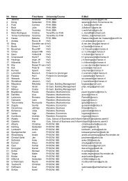
You also want an ePaper? Increase the reach of your titles
YUMPU automatically turns print PDFs into web optimized ePapers that Google loves.
AD538–SPECIFICATIONS<br />
(V S = 15 V, T A = +25C unless otherwise noted)<br />
AD538AD AD538BD AD538SD<br />
Parameters Conditions Min Typ Max Min Typ Max Min Typ Max Units<br />
MULTIPLIER DIVIDER<br />
PERFORMANCE<br />
Nominal Transfer<br />
Function<br />
⎛ V Z<br />
⎞<br />
10 V ≥ V X , V Y , V Z ≥ 0 V O = V Y ⎜ ⎟<br />
⎝ ⎠<br />
V X<br />
m<br />
⎛<br />
V O = Vy ⎜<br />
⎝<br />
m<br />
V Z<br />
⎞<br />
V<br />
⎟<br />
X ⎠<br />
⎛<br />
V O = V Y ⎜<br />
⎝<br />
m<br />
V Z<br />
⎞<br />
V<br />
⎟<br />
X ⎠<br />
m<br />
400 µA ≥ I X , I Y, I Z ≥ 0<br />
⎛ I Z<br />
⎞<br />
⎛ I<br />
V O = 25 kΩ × I Y ⎜<br />
⎝ I<br />
⎟ V O = 25 kΩ × I Z<br />
⎞<br />
⎛ I Z<br />
⎞<br />
Y ⎜<br />
X ⎠<br />
⎝ I<br />
⎟ V O = 25 kΩ × I Y ⎜<br />
X ⎠<br />
⎝ I<br />
⎟<br />
X ⎠<br />
Total Error Terms 100 mV ≤ V X ≤ 10 V ±0.5 1 ± 0.25 0.5 ± 0.5 1 % of Reading +<br />
100:1 Input Range 1 100 mV ≤ V Y ≤ 10 V ±200 500 ± 100 250 ± 200 500 µV<br />
100 mV ≤ V Z ≤ 10 V<br />
V Z ≤ 10 V X , m = 1.0<br />
T A = T MIN to T MAX ±1 2 ± 0.5 1 ± 1.25 2.5 % of Reading +<br />
±450 750 ± 350 500 ± 750 1000 µV<br />
Wide Dynamic Range 2 10 mV ≤ V X ≤ 10 V ±1 2 ± 0.5 1 ± 1 2 % of Reading +<br />
1 mV ≤ V Y ≤ 10 V ±200 500 ± 100 250 ± 200 500 µV +<br />
0 mV ≤ V Z ≤ 10 V ±100 250 ± 750 150 ± 200 250 µV × (V Y + V Z )/V X<br />
V Z ≤ 10 V X , m = 1.0<br />
T A = T MIN to T MAX ±1 3 ± 1 2 ± 2 4 % of Reading +<br />
±450 750 ± 350 500 ± 750 1000 µV +<br />
±450 750 ± 350 500 ± 750 1000 µV × (V Y + V Z )/V X<br />
Exponent (m) Range T A = T MIN to T MAX 0.2 5 0.2 5 0.2 5<br />
OUTPUT<br />
CHARACTERISTICS<br />
Offset Voltage V Y = 0, V C = –600 mV ±200 500 ± 100 250 ± 200 500 µV<br />
T A = T MIN to T MAX ±450 750 ± 350 500 ± 750 1000 µV<br />
Output Voltage Swing R L = 2 kΩ –11 +11 –11 +11 –11 +11 V<br />
Output Current 5 10 5 10 5 10 mA<br />
FREQUENCY RESPONSE<br />
Slew Rate 1.4 1.4 1.4 V/µs<br />
Small Signal Bandwidth 100 mV ≤ 10 V Y , V Z , 400 400 400 kHz<br />
V X ≤ 10 V<br />
VOLTAGE REFERENCE<br />
Accuracy V REF = 10 V or 2 V ±25 50 ± 15 25 ± 25 50 mV<br />
Additional Error T A = T MIN or T MAX ±20 30 ± 20 30 ± 30 50 mV<br />
Output Current V REF = 10 V to 2 V 1 2.5 1 2.5 1 2.5 mA<br />
Power Supply Rejection<br />
+2 V = V REF ±4.5 V ≤ V S ≤ ± 18 V 300 600 300 600 300 600 µV/V<br />
+10 V = V REF ±13 V ≤ V S ≤ ±18 V 200 500 200 500 200 500 µV/V<br />
POWER SUPPLY<br />
Rated R L = 2 kΩ ±15 ± 15 ± 15 V<br />
Operating Range 3 4.5 18 4.5 18 4.5 18 V<br />
PSRR ±4.5 V < V S < ±18 V 0.5 0.1 0.05 0.1 0.5 0.1 %/V<br />
V X = V Y = V Z = 1 V<br />
V OUT = 1 V<br />
Quiescent Current 4.5 7 4.5 7 4.5 7 mA<br />
TEMPERATURE RANGE<br />
Rated –25 +85 –25 +85 –55 +125 °C<br />
Storage –65 +150 –65 +150 –65 +150 °C<br />
PACKAGE OPTIONS<br />
Ceramic (D-18) AD538AD AD538BD AD538SD<br />
AD538SD/883B<br />
Chips<br />
AD538ACHIPS<br />
NOTES<br />
1 Over the 100 mV to 10 V operating range total error is the sum of a percent of reading term and an output offset. With this input dynamic range the input offset<br />
contribution to total error is negligible compared to the percent of reading error. Thus, it is specified indirectly as a part of the percent of reading error.<br />
2 The most accurate representation of total error with low level inputs is the summation of a percent of reading term, an output offset and an input offset multiplied by<br />
the incremental gain (V Y + V Z ) V X .<br />
3 When using supplies below ± 13 V, the 10 V reference pin must be connected to the 2 V pin in order for the AD538 to operate correctly.<br />
Specifications subject to change without notice.<br />
Specifications shown in boldface are tested on all production units at final electrical test. Results from those tests are used to calculate outgoing quality levels. All min<br />
and max specifications are guaranteed, although only those shown in boldface are tested on all production units.<br />
m<br />
m<br />
–2– REV. C