You also want an ePaper? Increase the reach of your titles
YUMPU automatically turns print PDFs into web optimized ePapers that Google loves.
AD538<br />
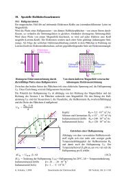
V O IN mV PEAK-TO-PEAK<br />
150<br />
100<br />
10<br />
1.0<br />
V X = 10V<br />
V Y = 5V +5V SIN t VOLTS<br />
V Z = 0V<br />
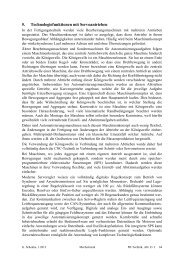
VOLTAGE NOISE, e n – V Hz<br />
100<br />
10<br />
1<br />
0.10<br />
FOR THE FREQUENCY RANGE OF 10Hz<br />
TO 100kHz THE TOTAL RMS OUTPUT<br />
NOISE, e o , FOR A GIVEN BANDWIDTH<br />
Bw, IS CALCULATED e o = e n Bw<br />
V X = 0.01V<br />
V X = 10V<br />
0.1<br />
100<br />
1k 10k 100k 1M<br />
INPUT FREQUENCY – Hz<br />
Figure 7. V Y Feedthrough vs. Frequency<br />
0.01<br />
0.01<br />
0.1 1 10<br />
DC OUTPUT VOLTAGE – Volts<br />
Figure 8. 1 kHz Output Noise Spectral Density vs. DC Output<br />
Voltage<br />
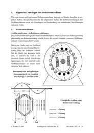
I Z 1 18 A<br />
25k<br />
LOG<br />
V Z 2<br />
RATIO<br />
17 D<br />
B 3<br />
16 I X<br />
+10V 4<br />
15 V X<br />
25k<br />
100 100<br />
+2V 5<br />
14<br />
INTERNAL<br />
VOLTAGE<br />
+V S 6<br />
REFERENCE AD538<br />
13<br />
–V S 7 OUTPUT<br />
12 C<br />
25k<br />
V O 8<br />
11 I Y<br />
ANTILOG<br />
I<br />
9<br />
LOG<br />
PWR<br />
GND<br />
10 V Y<br />
25k<br />
Figure 9. Functional Block Diagram<br />
SIGNAL<br />
GND<br />
FUNCTIONAL DESCRIPTION<br />
As shown in Figures 9 and 10, the V Z and V X inputs connect<br />
directly to the AD538’s input log ratio amplifiers. This subsection<br />
provides an output voltage proportional to the natural log<br />
of input voltage V Z , minus the natural log of input voltage V X .<br />
The output of the log ratio subsection at B can be expressed by<br />
the transfer function:<br />
V B = kT q ln ⎛ V Z<br />
⎞<br />
⎜ ⎟<br />
⎝ ⎠<br />
V X<br />
where k = 1.3806 × 10 –23 J/K,<br />
q = 1.60219 × 10 –19 C,<br />
T is in Kelvins.<br />
The log ratio configuration may be used alone, if correctly temperature<br />
compensated and scaled to the desired output level<br />
(see Applications section).<br />
Under normal operation, the log-ratio output will be directly<br />
connected to a second functional block at input C, the antilog<br />
subsection. This section performs the antilog according to the<br />
transfer function:<br />
⎛<br />
⎜<br />
V O = V Y e V C<br />
⎝<br />
q ⎞<br />
kT<br />
⎟<br />
⎠<br />
As with the log-ratio circuit included in the AD538, the user<br />
may use the antilog subsection by itself. When both subsections<br />
are combined, the output at B is tied to C, the transfer function<br />
of the AD538 computational unit is:<br />
which reduces to:<br />
V O = V Y e<br />
⎡⎛<br />
⎢⎜<br />
⎣⎢<br />
⎝<br />
V<br />
kT<br />
q<br />
O<br />
⎞ ⎛ q ⎞<br />
⎟ ⎜<br />
⎠ ⎝ kT<br />
⎟<br />
⎠<br />
ln ⎛ V Z ⎞ ⎤<br />
⎜<br />
⎝ V<br />
⎟ ⎥<br />
X ⎠ ⎦<br />
= V<br />
Y<br />
⎛VZ<br />
⎞<br />
⎜<br />
⎝V<br />
⎟<br />
X ⎠<br />
⎥<br />
; V B<br />
= V C<br />
Finally, by increasing the gain, or attenuating the output of the<br />
log ratio subsection via resistor programming, it is possible to<br />
raise the quantity V Z /V X to the m th power. Without external<br />
programming, m is unity. Thus the overall AD538 transfer<br />
function equals:<br />
V O = V Y<br />
⎛<br />
⎜<br />
⎝<br />
V Z<br />
V X<br />
where 0.2 < m < 5.<br />
When the AD538 is used as an analog divider, the V Y input can<br />
be used to multiply the ratio V Z /V X by a convenient scale factor.<br />
The actual multiplication by the V Y input signal is accomplished<br />
by adding the log of the V Y input signal to the signal at C, which<br />
is already in the log domain.<br />
⎞<br />
⎟<br />
⎠<br />
m<br />
–6– REV. C