You also want an ePaper? Increase the reach of your titles
YUMPU automatically turns print PDFs into web optimized ePapers that Google loves.
AD538<br />
TWO-QUADRANT DIVISION<br />
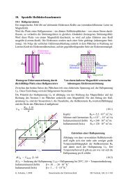
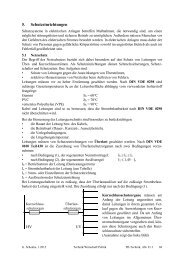
The two-quadrant linear divider circuit illustrated in Figure 13<br />
uses the same basic connections as the one-quadrant version.<br />
However, in this circuit the numerator has been offset in the<br />
positive direction by adding the denominator input voltage to it.<br />
The offsetting scheme changes the divider’s transfer function<br />
from:<br />
to:<br />
V O = 10V<br />
V O<br />
(<br />
= 10V V Z + AV X )<br />
⎛<br />
⎜<br />
⎝<br />
V Z<br />
V X<br />
⎞<br />
⎟<br />
⎠<br />
⎛<br />
= 10 V 1 A + V ⎞<br />
Z<br />
⎜ ⎟<br />
V X ⎝ ⎠<br />
V X<br />
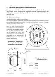
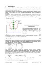
LOG RATIO OPERATION<br />
Figure 14 shows the AD538 configured for computing the log of<br />
the ratio of two input voltages (or currents). The output signal<br />
from B is connected to the summing junction of the output amplifier<br />
via two series resistors. The 90.9 Ω metal film resistor effectively<br />
degrades the temperature coefficient of the ± 3500 ppm/°C<br />
resistor to produce a 1.09 kΩ +3300 ppm/°C equivalent value.<br />
In this configuration, the V Y input must be tied to some voltage<br />
less than zero (–1.2 V in this case) removing this input from the<br />
transfer function.<br />
The 5 kΩ potentiometer controls the circuit’s scale factor adjustment<br />
providing a +1 V per decade adjustment. The output<br />
offset potentiometer should be set to provide a zero output with<br />
V X = V Z = 1 V. The input V Z adjustment should be set for an<br />
output of 3 V with V Z = l mV and V X = 1 V.<br />
⎛<br />
= 10 A +10 V V ⎞<br />
Z<br />
⎜ ⎟<br />
⎝ ⎠<br />
V X<br />
–V S<br />
68k<br />
5%<br />
AD589<br />
–1.2V<br />
V<br />
V O = 1V LOG 10 ( Z<br />
)<br />
V X<br />
⎛ 35 kΩ ⎞<br />
where A = ⎜<br />
⎝ 25 kΩ<br />
⎟<br />
⎠<br />
As long as the magnitude of the denominator input is equal to<br />
or greater than the magnitude of the numerator input, the circuit<br />
will accept bipolar numerator voltages. However, under the<br />
conditions of a 0 V numerator input, the output would incorrectly<br />
equal +14 V. The offset can be removed by connecting<br />
the +10 V reference through resistors R1 and R2 to the output<br />
section’s summing node I at Pin 9 thus providing a gain of 1.4<br />
at the center of the trimming potentiometer. The pot R2 adjusts<br />
out or corrects this offset, leaving the desired transfer function<br />
of 10 V (V Z /V X ).<br />
OPTIONAL<br />
INPUT V OS<br />
ADJUSTMENT<br />
90.9<br />
1%<br />
10M I Z<br />
1M<br />
1<br />
V Z 25k<br />
2<br />
B<br />
3<br />
+10V<br />
4<br />
100<br />
+2V<br />
5<br />
1k<br />
+3500<br />
ppm/C<br />
OUTPUT<br />
5k<br />
SCALE<br />
FACTOR<br />
ADJUST<br />
2k<br />
1%<br />
+15V 6<br />
–15V 7<br />
V O<br />
8<br />
I<br />
9<br />
OUTPUT<br />
25k<br />
LOG<br />
RATIO<br />
INTERNAL<br />
VOLTAGE<br />
REFERENCE<br />
ANTILOG<br />
LOG<br />
100<br />
AD538<br />
A<br />
18<br />
48.7<br />
D<br />
17<br />
16 I X V X<br />
V X INPUT<br />
15<br />
25k SIGNAL<br />
GND<br />
14<br />
PWR<br />
GND<br />
13<br />
C<br />
12<br />
I Y<br />
11<br />
IN4148<br />
V Y<br />
10<br />
25k<br />
NUMERATOR<br />
OPTIONAL V Z<br />
Z OFFSET TRIM<br />
AD589<br />
1M<br />
V OS ADJ<br />
OUTPUT<br />
–V S<br />
68k<br />
5%<br />
–1.2V<br />
10M<br />
3.9M<br />
+15V<br />
I Z<br />
1<br />
V Z 25k<br />
2<br />
B<br />
3<br />
+10V<br />
4<br />
100<br />
+2V 5<br />
6<br />
–15V 7<br />
V O<br />
8<br />
R2 R1<br />
10k 12.4k I<br />
9<br />
ZERO<br />
ADJUST<br />
35k<br />
OUTPUT<br />
25k<br />
DENOMINATOR<br />
V X<br />
18 A<br />
LOG<br />
35k<br />
RATIO<br />
17 D<br />
I X<br />
16<br />
15 V X<br />
100<br />
25k SIGNAL<br />
GND<br />
14<br />
PWR<br />
AD538<br />
GND<br />
13<br />
IN4148<br />
C<br />
12<br />
I Y<br />
11<br />
ANTILOG<br />
V Y<br />
LOG<br />
10<br />
25k<br />
V<br />
V OUT = 10 ( Z<br />
FOR<br />
) V<br />
V X V Z<br />
X<br />
INTERNAL<br />
VOLTAGE<br />
REFERENCE<br />
10M<br />
+V S<br />
10k<br />
–V S<br />
OPTIONAL<br />
OUTPUT V OS<br />
ADJUSTMENT<br />
Figure 14. Log Ratio Circuit<br />
The log ratio circuit shown achieves ±0.5% accuracy in the log<br />
domain for input voltages within three decades of input range:<br />
10 mV to 10 V. This error is not defined as a percent of fullscale<br />
output, but as a percent of input. For example, using a<br />
1 V/decade scale factor, a 1% error in the positive direction at<br />
the INPUT of the log ratio amplifier translates into a 4.3 mV<br />
deviation from the ideal OUTPUT (i.e., 1 V × log 10 (1.01) =<br />
4.3214 mV). An input error 1% in the negative direction is<br />
slightly different, giving an output deviation of 4.3648 mV.<br />
Figure 13. Two-Quadrant Division with 10 V Scaling<br />
–8– REV. C