
You also want an ePaper? Increase the reach of your titles
YUMPU automatically turns print PDFs into web optimized ePapers that Google loves.
a<br />
FEATURES<br />
m<br />
⎛ V Z ⎞<br />
V OUT = V Y ⎜<br />
⎝ V<br />
⎟ Transfer Function<br />
X ⎠<br />
Wide Dynamic Range (Denominator) –1000:1<br />
Simultaneous Multiplication and Division<br />
Resistor-Programmable Powers and Roots<br />
No External Trims Required<br />
Low Input Offsets
AD538–SPECIFICATIONS<br />
(V S = 15 V, T A = +25C unless otherwise noted)<br />
AD538AD AD538BD AD538SD<br />
Parameters Conditions Min Typ Max Min Typ Max Min Typ Max Units<br />
MULTIPLIER DIVIDER<br />
PERFORMANCE<br />
Nominal Transfer<br />
Function<br />
⎛ V Z<br />
⎞<br />
10 V ≥ V X , V Y , V Z ≥ 0 V O = V Y ⎜ ⎟<br />
⎝ ⎠<br />
V X<br />
m<br />
⎛<br />
V O = Vy ⎜<br />
⎝<br />
m<br />
V Z<br />
⎞<br />
V<br />
⎟<br />
X ⎠<br />
⎛<br />
V O = V Y ⎜<br />
⎝<br />
m<br />
V Z<br />
⎞<br />
V<br />
⎟<br />
X ⎠<br />
m<br />
400 µA ≥ I X , I Y, I Z ≥ 0<br />
⎛ I Z<br />
⎞<br />
⎛ I<br />
V O = 25 kΩ × I Y ⎜<br />
⎝ I<br />
⎟ V O = 25 kΩ × I Z<br />
⎞<br />
⎛ I Z<br />
⎞<br />
Y ⎜<br />
X ⎠<br />
⎝ I<br />
⎟ V O = 25 kΩ × I Y ⎜<br />
X ⎠<br />
⎝ I<br />
⎟<br />
X ⎠<br />
Total Error Terms 100 mV ≤ V X ≤ 10 V ±0.5 1 ± 0.25 0.5 ± 0.5 1 % of Reading +<br />
100:1 Input Range 1 100 mV ≤ V Y ≤ 10 V ±200 500 ± 100 250 ± 200 500 µV<br />
100 mV ≤ V Z ≤ 10 V<br />
V Z ≤ 10 V X , m = 1.0<br />
T A = T MIN to T MAX ±1 2 ± 0.5 1 ± 1.25 2.5 % of Reading +<br />
±450 750 ± 350 500 ± 750 1000 µV<br />
Wide Dynamic Range 2 10 mV ≤ V X ≤ 10 V ±1 2 ± 0.5 1 ± 1 2 % of Reading +<br />
1 mV ≤ V Y ≤ 10 V ±200 500 ± 100 250 ± 200 500 µV +<br />
0 mV ≤ V Z ≤ 10 V ±100 250 ± 750 150 ± 200 250 µV × (V Y + V Z )/V X<br />
V Z ≤ 10 V X , m = 1.0<br />
T A = T MIN to T MAX ±1 3 ± 1 2 ± 2 4 % of Reading +<br />
±450 750 ± 350 500 ± 750 1000 µV +<br />
±450 750 ± 350 500 ± 750 1000 µV × (V Y + V Z )/V X<br />
Exponent (m) Range T A = T MIN to T MAX 0.2 5 0.2 5 0.2 5<br />
OUTPUT<br />
CHARACTERISTICS<br />
Offset Voltage V Y = 0, V C = –600 mV ±200 500 ± 100 250 ± 200 500 µV<br />
T A = T MIN to T MAX ±450 750 ± 350 500 ± 750 1000 µV<br />
Output Voltage Swing R L = 2 kΩ –11 +11 –11 +11 –11 +11 V<br />
Output Current 5 10 5 10 5 10 mA<br />
FREQUENCY RESPONSE<br />
Slew Rate 1.4 1.4 1.4 V/µs<br />
Small Signal Bandwidth 100 mV ≤ 10 V Y , V Z , 400 400 400 kHz<br />
V X ≤ 10 V<br />
VOLTAGE REFERENCE<br />
Accuracy V REF = 10 V or 2 V ±25 50 ± 15 25 ± 25 50 mV<br />
Additional Error T A = T MIN or T MAX ±20 30 ± 20 30 ± 30 50 mV<br />
Output Current V REF = 10 V to 2 V 1 2.5 1 2.5 1 2.5 mA<br />
Power Supply Rejection<br />
+2 V = V REF ±4.5 V ≤ V S ≤ ± 18 V 300 600 300 600 300 600 µV/V<br />
+10 V = V REF ±13 V ≤ V S ≤ ±18 V 200 500 200 500 200 500 µV/V<br />
POWER SUPPLY<br />
Rated R L = 2 kΩ ±15 ± 15 ± 15 V<br />
Operating Range 3 4.5 18 4.5 18 4.5 18 V<br />
PSRR ±4.5 V < V S < ±18 V 0.5 0.1 0.05 0.1 0.5 0.1 %/V<br />
V X = V Y = V Z = 1 V<br />
V OUT = 1 V<br />
Quiescent Current 4.5 7 4.5 7 4.5 7 mA<br />
TEMPERATURE RANGE<br />
Rated –25 +85 –25 +85 –55 +125 °C<br />
Storage –65 +150 –65 +150 –65 +150 °C<br />
PACKAGE OPTIONS<br />
Ceramic (D-18) AD538AD AD538BD AD538SD<br />
AD538SD/883B<br />
Chips<br />
AD538ACHIPS<br />
NOTES<br />
1 Over the 100 mV to 10 V operating range total error is the sum of a percent of reading term and an output offset. With this input dynamic range the input offset<br />
contribution to total error is negligible compared to the percent of reading error. Thus, it is specified indirectly as a part of the percent of reading error.<br />
2 The most accurate representation of total error with low level inputs is the summation of a percent of reading term, an output offset and an input offset multiplied by<br />
the incremental gain (V Y + V Z ) V X .<br />
3 When using supplies below ± 13 V, the 10 V reference pin must be connected to the 2 V pin in order for the AD538 to operate correctly.<br />
Specifications subject to change without notice.<br />
Specifications shown in boldface are tested on all production units at final electrical test. Results from those tests are used to calculate outgoing quality levels. All min<br />
and max specifications are guaranteed, although only those shown in boldface are tested on all production units.<br />
m<br />
m<br />
–2– REV. C
AD538<br />
RE-EXAMINATION OF MULTIPLIER/DIVIDER<br />
ACCURACY<br />
Traditionally, the “accuracy” (actually the errors) of analog<br />
multipliers and dividers have been specified in terms of percent<br />
of full scale. Thus specified, a 1% multiplier error with a 10 V<br />
full-scale output would mean a worst case error of +100 mV at<br />
“any” level within its designated output range. While this type<br />
of error specification is easy to test evaluate, and interpret, it can<br />
leave the user guessing as to how useful the multiplier actually is<br />
at low output levels, those approaching the specified error limit<br />
(in this case) 100 mV.<br />
The AD538’s error sources do not follow the percent of fullscale<br />
approach to specification, thus it more optimally fits the<br />
needs of the very wide dynamic range applications for which it is<br />
best suited. Rather than as a percent of full scale, the AD538’s<br />
error as a multiplier or divider for a 100:1 (100 mV to 10 V)<br />
input range is specified as the sum of two error components: a<br />
percent of reading (ideal output) term plus a fixed output offset.<br />
Following this format the AD538AD, operating as a multiplier<br />
or divider with inputs down to 100 mV, has a maximum error of<br />
± 1% of reading ± 500 µV. Some sample total error calculations<br />
for both grades over the 100:1 input range are illustrated in the<br />
chart below. This error specification format is a familiar one to<br />
designers and users of digital voltmeters where error is specified<br />
as a percent of reading ± a certain number of digits on the meter<br />
readout.<br />
For operation as a multiplier or divider over a wider dynamic<br />
range (>100:1), the AD538 has a more detailed error specification<br />
that is the sum of three components: a percent of reading<br />
term, an output offset term and an input offset term for the<br />
V Y /V X log ratio section. A sample application of this specification,<br />
taken from Table I, for the AD538AD with V Y = 1 V, V Z =<br />
100 mV and V X = 10 mV would yield a maximum error of<br />
± 2.0% of reading ± 500 µV ± (1 V + 100 mV)/10 mV × 250 µV<br />
or ± 2.0% of reading ±500 µV ± 27.5 mV. This example illustrates<br />
that with very low level inputs the AD538’s incremental<br />
gain (V Y + V Z )/V X has increased to make the input offset contribution<br />
to error substantial.<br />
Table I. Sample Error Calculation Chart (Worst Case)<br />
±<br />
V Y V Z V X Ideal Total Offset % of Reading Total Error Total Error Summation<br />
Input Input Input Output Error Term Error Term Summation as a % of the Ideal<br />
(in V) (in V) (in V) (in V) (in mV) (in mV) (in mV) Output<br />
100:1 10 10 10 10 0.5 (AD) 100 (AD) 100.5 (AD) 1.0 (AD)<br />
INPUT 0.25 (BD) 50 (BD) 50.25 (BD) 0.5 (BD)<br />
RANGE<br />
Total Error = 10 0.1 0.1 10 0.5 (AD) 100 (AD) 100.5 (AD) 1.0 (AD)<br />
± % rdg 0.25 (BD) 50 (BD) 50.25 (BD) 0.5 (BD)<br />
Output V OS<br />
1 1 1 1 0.5 (AD) 10 (AD) 10.5 (AD) 1.05 (AD)<br />
0.25 (BD) 5 (BD) 5.25 (BD) 0.5 (BD)<br />
0.1 0.1 0.1 0.1 0.5 (AD) 1 (AD) 1.5 (AD) 1.5 (AD)<br />
0.25 (BD) 0.5 (BD) 0.75 (BD) 0.75 (BD)<br />
WIDE 1 0.10 0.01 10 28 (AD) 200 (AD) 228 (AD) 2.28 (AD)<br />
DYNAMIC 16.75 (BD) 100 (BD) 116.75 (BD) 1.17 (BD)<br />
RANGE<br />
Total Error = 10 0.05 2 0.25 1.76 (AD) 5 (AD) 6.76 (AD) 2.7 (AD)<br />
± % rdg 1 (BD) 2.5 (BD) 3.5 (BD) 1.4 (BD)<br />
± Output V OS<br />
± Input V OS × 5 0.01 0.01 5 125.75 (AD) 100 (AD) 225.75 (AD) 4.52 (AD)<br />
(V Y + V Z )/V X 75.4 (BD) 50 (BD) 125.4 (BD) 2.51 (BD)<br />
10 0.01 0.1 1 25.53 (AD) 20 (AD) 45.53 (AD) 4.55 (AD)<br />
15.27 (BD) 10 (BD) 25.27 (BD) 2.53 (BD)<br />
REV. C<br />
–3–
AD538<br />
ABSOLUTE MAXIMUM RATINGS<br />
Supply Voltage . . . . . . . . . . . . . . . . . . . . . . . . . . . . . . . ± 18 V<br />
Internal Power Dissipation . . . . . . . . . . . . . . . . . . . . 250 mW<br />
Output Short Circuit-to-Ground . . . . . . . . . . . . . . . Indefinite<br />
Input Voltages V X , V Y , V Z . . . . . . . . . . . . . (+V S – 1 V), –1 V<br />
Input Currents I X , I Y , I Z , I O . . . . . . . . . . . . . . . . . . . . . . 1 mA<br />
Operating Temperature Range . . . . . . . . . . . –25°C to +85°C<br />
Storage Temperature Range . . . . . . . . . . . . –65°C to +150°C<br />
Lead Temperature, Storage . . . . . . . . . . . . . . 60 sec, +300°C<br />
Thermal Resistance<br />
θ JC . . . . . . . . . . . . . . . . . . . . . . . . . . . . . . . . . . . . . 35°C/W<br />
θ JA . . . . . . . . . . . . . . . . . . . . . . . . . . . . . . . . . . . . 120°C/W<br />
PIN CONFIGURATION<br />
I Z<br />
V Z<br />
1<br />
2<br />
B 3<br />
+10V 4<br />
18 A<br />
17 D<br />
16 I X<br />
15 V X<br />
+2V 5 TOP VIEW<br />
(Not to Scale)<br />
14 SIGNAL GND<br />
+V S<br />
–V S<br />
6<br />
7<br />
13<br />
12<br />
PWR GND<br />
C<br />
V O<br />
I<br />
AD538<br />
8 11 I Y<br />
9 10 V Y<br />
ORDERING GUIDE<br />
Temperature Package Package<br />
Model Range Description Option<br />
AD538AD –25°C to +85°C Side-Brazed Ceramic DIP D-18<br />
AD538BD –25°C to +85°C Side-Brazed Ceramic DIP D-18<br />
AD538ACHIPS –25°C to +85°C Chips<br />
AD538SD –55°C to +125°C Side-Brazed Ceramic DIP D-18<br />
AD538SD/883B –55°C to +125°C Side-Brazed Ceramic DIP D-18<br />
CAUTION<br />
ESD (electrostatic discharge) sensitive device. Electrostatic charges as high as 4000 V readily<br />
accumulate on the human body and test equipment and can discharge without detection.<br />
Although the AD538 features proprietary ESD protection circuitry, permanent damage may<br />
occur on devices subjected to high energy electrostatic discharges. Therefore, proper ESD<br />
precautions are recommended to avoid performance degradation or loss of functionality.<br />
WARNING!<br />
ESD SENSITIVE DEVICE<br />
–4– REV. C
5.0<br />
1000<br />
Typical Performance Characteristics– AD538<br />
1M<br />
TOTAL % OF READING ERROR<br />
4.0<br />
3.0<br />
2.0<br />
1.0<br />
OFFSET<br />
800<br />
600<br />
400<br />
200<br />
OUTPUT STAGE OFFSET – V<br />
SMALL SIGNAL BANDWITH – Hz<br />
400k<br />
100k<br />
40k<br />
V Y = 10V dc<br />
V Z = V X +0.05 V X SIN t<br />
% OF READING<br />
0<br />
0<br />
–55 –40 –20 0 20 40 60 80 100 125<br />
TEMPERATURE – C<br />
10k<br />
0.01<br />
0.1 1 10<br />
DENOMINATOR VOLTAGE, V X – V dc<br />
Figure 1. Multiplier Error vs. Temperature<br />
(100 mV < V X , V Y , V Z ≤ 10 V)<br />
Figure 4. Small Signal Bandwidth vs. Denominator<br />
Voltage (One-Quadrant Mult/Div)<br />
5.0<br />
1000<br />
6.0<br />
1200<br />
TOTAL % OF READING ERROR<br />
4.0<br />
3.0<br />
2.0<br />
1.0<br />
OFFSET<br />
% OF READING<br />
0<br />
0<br />
–55 –40 –20 0 20 40 60 80 100 125<br />
TEMPERATURE – C<br />
Figure 2. Divider Error vs. Temperature<br />
(100 mV < V X , V Y , V Z ≤ 10 V)<br />
800<br />
600<br />
400<br />
200<br />
OUTPUT STAGE OFFSET – V<br />
TOTAL % OF READING ERROR<br />
5.0<br />
4.0<br />
3.0<br />
2.0<br />
1.0<br />
% OF READING<br />
OFFSET<br />
0<br />
0<br />
–55 –40 –20 0 20 40 60 80 100 125<br />
TEMPERATURE – C<br />
Figure 5. Multiplier Error vs. Temperature<br />
(10 mV < V X , V Y , V Z ≤ 100 mV)<br />
1000<br />
800<br />
600<br />
400<br />
200<br />
OUTPUT STAGE OFFSET – V<br />
V O IN mV PEAK-TO-PEAK<br />
1000<br />
100<br />
10<br />
V X = 10V<br />
V Y = 0V<br />
V Z = 5V +5V SIN t VOLTS<br />
TOTAL % OF READING ERROR<br />
5.0<br />
4.0<br />
3.0<br />
2.0<br />
1.0<br />
% OF READING<br />
1000<br />
800<br />
600<br />
400<br />
200<br />
OUTPUT STAGE OFFSET – V<br />
1<br />
100<br />
1k 10k 100k 1M<br />
INPUT FREQUENCY – Hz<br />
Figure 3. V Z Feedthrough vs. Frequency<br />
OFFSET<br />
0<br />
0<br />
–55 –40 –20 0 20 40 60 80 100 125<br />
TEMPERATURE – C<br />
Figure 6. Divider Error vs. Temperature<br />
(10 mV < V X , V Y , V Z ≤ 100 mV)<br />
REV. C<br />
–5–
AD538<br />
V O IN mV PEAK-TO-PEAK<br />
150<br />
100<br />
10<br />
1.0<br />
V X = 10V<br />
V Y = 5V +5V SIN t VOLTS<br />
V Z = 0V<br />
VOLTAGE NOISE, e n – V Hz<br />
100<br />
10<br />
1<br />
0.10<br />
FOR THE FREQUENCY RANGE OF 10Hz<br />
TO 100kHz THE TOTAL RMS OUTPUT<br />
NOISE, e o , FOR A GIVEN BANDWIDTH<br />
Bw, IS CALCULATED e o = e n Bw<br />
V X = 0.01V<br />
V X = 10V<br />
0.1<br />
100<br />
1k 10k 100k 1M<br />
INPUT FREQUENCY – Hz<br />
Figure 7. V Y Feedthrough vs. Frequency<br />
0.01<br />
0.01<br />
0.1 1 10<br />
DC OUTPUT VOLTAGE – Volts<br />
Figure 8. 1 kHz Output Noise Spectral Density vs. DC Output<br />
Voltage<br />
I Z 1 18 A<br />
25k<br />
LOG<br />
V Z 2<br />
RATIO<br />
17 D<br />
B 3<br />
16 I X<br />
+10V 4<br />
15 V X<br />
25k<br />
100 100<br />
+2V 5<br />
14<br />
INTERNAL<br />
VOLTAGE<br />
+V S 6<br />
REFERENCE AD538<br />
13<br />
–V S 7 OUTPUT<br />
12 C<br />
25k<br />
V O 8<br />
11 I Y<br />
ANTILOG<br />
I<br />
9<br />
LOG<br />
PWR<br />
GND<br />
10 V Y<br />
25k<br />
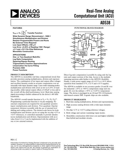
Figure 9. Functional Block Diagram<br />
SIGNAL<br />
GND<br />
FUNCTIONAL DESCRIPTION<br />
As shown in Figures 9 and 10, the V Z and V X inputs connect<br />
directly to the AD538’s input log ratio amplifiers. This subsection<br />
provides an output voltage proportional to the natural log<br />
of input voltage V Z , minus the natural log of input voltage V X .<br />
The output of the log ratio subsection at B can be expressed by<br />
the transfer function:<br />
V B = kT q ln ⎛ V Z<br />
⎞<br />
⎜ ⎟<br />
⎝ ⎠<br />
V X<br />
where k = 1.3806 × 10 –23 J/K,<br />
q = 1.60219 × 10 –19 C,<br />
T is in Kelvins.<br />
The log ratio configuration may be used alone, if correctly temperature<br />
compensated and scaled to the desired output level<br />
(see Applications section).<br />
Under normal operation, the log-ratio output will be directly<br />
connected to a second functional block at input C, the antilog<br />
subsection. This section performs the antilog according to the<br />
transfer function:<br />
⎛<br />
⎜<br />
V O = V Y e V C<br />
⎝<br />
q ⎞<br />
kT<br />
⎟<br />
⎠<br />
As with the log-ratio circuit included in the AD538, the user<br />
may use the antilog subsection by itself. When both subsections<br />
are combined, the output at B is tied to C, the transfer function<br />
of the AD538 computational unit is:<br />
which reduces to:<br />
V O = V Y e<br />
⎡⎛<br />
⎢⎜<br />
⎣⎢<br />
⎝<br />
V<br />
kT<br />
q<br />
O<br />
⎞ ⎛ q ⎞<br />
⎟ ⎜<br />
⎠ ⎝ kT<br />
⎟<br />
⎠<br />
ln ⎛ V Z ⎞ ⎤<br />
⎜<br />
⎝ V<br />
⎟ ⎥<br />
X ⎠ ⎦<br />
= V<br />
Y<br />
⎛VZ<br />
⎞<br />
⎜<br />
⎝V<br />
⎟<br />
X ⎠<br />
⎥<br />
; V B<br />
= V C<br />
Finally, by increasing the gain, or attenuating the output of the<br />
log ratio subsection via resistor programming, it is possible to<br />
raise the quantity V Z /V X to the m th power. Without external<br />
programming, m is unity. Thus the overall AD538 transfer<br />
function equals:<br />
V O = V Y<br />
⎛<br />
⎜<br />
⎝<br />
V Z<br />
V X<br />
where 0.2 < m < 5.<br />
When the AD538 is used as an analog divider, the V Y input can<br />
be used to multiply the ratio V Z /V X by a convenient scale factor.<br />
The actual multiplication by the V Y input signal is accomplished<br />
by adding the log of the V Y input signal to the signal at C, which<br />
is already in the log domain.<br />
⎞<br />
⎟<br />
⎠<br />
m<br />
–6– REV. C
AD538<br />
STABILITY PRECAUTIONS<br />
At higher frequencies, the multistaged signal path of the AD538,<br />
as illustrated in Figure 10, can result in large phase shifts. If a<br />
condition of high incremental gain exists along that path (e.g.,<br />
V O = V Y × V Z /V X = 10 V × 10 mV/10 mV = 10 V so that<br />
∆V O /∆V X = 1000), then small amounts of capacitive feedback<br />
from V O to the current inputs I Z or I X can result in instability.<br />
Appropriate care should be exercised in board layout to prevent<br />
capacitive feedback mechanisms under these conditions.<br />
I X<br />
V X<br />
I Z<br />
V Z<br />
LOG e<br />
LOG e<br />
Ln Z – Ln X<br />
Ln X<br />
M(Ln Z – Ln X)<br />
M(Ln Z – Ln X) +Ln Y<br />
–<br />
0.2M5<br />
+ <br />
+ +<br />
Ln Z<br />
I Y<br />
V Y<br />
LOG e<br />
Ln Y<br />
ANTILOG e<br />
Figure 10. Model Circuit<br />
BUFFER<br />
V O = V Y<br />
V M Z<br />
V X<br />
USING THE VOLTAGE REFERENCES<br />
A stable bandgap voltage reference for scaling is included in the<br />
AD538. It is laser-trimmed to provide a selectable voltage output<br />
of +10 V buffered (Pin 4), +2 V unbuffered (Pin 5) or any<br />
voltages between +2 V and +10.2 V buffered as shown in Figure<br />
11. The output impedance at Pin 5 is approximately 5 kΩ. Note<br />
that any loading of this pin will produce an error in the +10 V<br />
reference voltage. External loads on the +2 V output should be<br />
greater than 500 kΩ to maintain errors less than 1%.<br />
+2V TO +10.2V<br />
BUFFERED<br />
50k<br />
11.5k<br />
I Z 1 18 A<br />
25k<br />
LOG<br />
V Z 2<br />
RATIO<br />
17 D<br />
B 3<br />
16 I X<br />
REF OUT<br />
4<br />
15 V X<br />
25k<br />
100 100<br />
+2V<br />
5<br />
14<br />
INTERNAL<br />
VOLTAGE<br />
+V S 6 REFERENCE AD538<br />
13<br />
–V S 7 OUTPUT<br />
12 C<br />
25k<br />
V O 8<br />
11 I Y<br />
ANTILOG<br />
I<br />
9<br />
LOG<br />
PWR<br />
GND<br />
10 V Y<br />
25k<br />
SIGNAL<br />
GND<br />
Figure 11. +2 V to +10.2 V Adjustable Reference<br />
In situations not requiring both reference levels, the +2 V output<br />
can be converted to a buffered output by tying Pins 4 and 5<br />
together. If both references are required simultaneously, the<br />
+10 V output should be used directly and the +2 V output<br />
should be externally buffered.<br />
ONE-QUADRANT MULTIPLICATION/DIVISION<br />
Figure 12 shows how the AD538 may be easily configured as a<br />
precision one-quadrant multiplier/divider. The transfer function<br />
V OUT = V Y (V Z /V X ) allows “three” independent input variables,<br />
a calculation not available with a conventional multiplier. In<br />
addition, the 1000:1 (i.e., 10 mV to 10 V) input dynamic range<br />
of the AD538 greatly exceeds that of analog multipliers computing<br />
one-quadrant multiplication and division.<br />
V<br />
V OUT = V Y ( Z<br />
V X<br />
)<br />
I Z 1 18 A<br />
V 25k<br />
LOG<br />
Z<br />
V Z<br />
2<br />
RATIO<br />
17 D<br />
INPUT<br />
B<br />
3<br />
16 I X<br />
V X<br />
+10V 4<br />
15<br />
25k<br />
100 100<br />
SIGNAL<br />
GND<br />
+2V 5<br />
14<br />
INTERNAL<br />
PWR<br />
VOLTAGE<br />
GND<br />
+15V 6 REFERENCE AD538<br />
13<br />
C<br />
–15V 7 OUTPUT<br />
12<br />
25k<br />
IN4148<br />
V O<br />
I Y<br />
8<br />
11<br />
OUTPUT<br />
ANTILOG<br />
V Y<br />
I 9<br />
LOG<br />
10<br />
25k<br />
V X<br />
INPUT<br />
V Y<br />
INPUT<br />
Figure 12. One-Quadrant Combination Multiplier/Divider<br />
By simply connecting the input V X (Pin 15) to the +10 V reference<br />
(Pin 4), and tying the log-ratio output at B to the antilog<br />
input at C, the AD538 can be configured as a one-quadrant<br />
analog multiplier with 10-volt scaling. If 2-volt scaling is desired,<br />
V X can be tied to the +2 V reference.<br />
When the input V X is tied to the +10 V reference terminal, the<br />
multiplier transfer function becomes:<br />
V O = V Y<br />
⎛ V Z<br />
⎞<br />
⎜<br />
⎝ 10 V<br />
⎟<br />
⎠<br />
As a multiplier, this circuit provides a typical bandwidth of<br />
400 kHz with values of V X , V Y or V Z varying over a 100:1 range<br />
(i.e., 100 mV to 10 V). The maximum error with a 100 mV to<br />
10 V range for the two input variables will typically be +0.5% of<br />
reading. Using the optional Z offset trim scheme, as shown in<br />
Figure 13, this error can be reduced to +0.25% of reading.<br />
By using the +10 V reference as the V Y input, the circuit of<br />
Figure 12 is configured as a one-quadrant divider with a fixed<br />
scale factor. As with the one-quadrant multiplier, the inputs<br />
accept only single (positive) polarity signals. The output of the<br />
one-quadrant divider with a +10 V scale factor is:<br />
V O = 10V<br />
⎛<br />
⎜<br />
⎝<br />
V Z<br />
V X<br />
The typical bandwidth of this circuit is 370 kHz with 1 V to<br />
10 V denominator input levels. At lower amplitudes, the bandwidth<br />
gradually decreases to approximately 200 kHz at the<br />
2 mV input level.<br />
⎞<br />
⎟<br />
⎠<br />
REV. C<br />
–7–
AD538<br />
TWO-QUADRANT DIVISION<br />
The two-quadrant linear divider circuit illustrated in Figure 13<br />
uses the same basic connections as the one-quadrant version.<br />
However, in this circuit the numerator has been offset in the<br />
positive direction by adding the denominator input voltage to it.<br />
The offsetting scheme changes the divider’s transfer function<br />
from:<br />
to:<br />
V O = 10V<br />
V O<br />
(<br />
= 10V V Z + AV X )<br />
⎛<br />
⎜<br />
⎝<br />
V Z<br />
V X<br />
⎞<br />
⎟<br />
⎠<br />
⎛<br />
= 10 V 1 A + V ⎞<br />
Z<br />
⎜ ⎟<br />
V X ⎝ ⎠<br />
V X<br />
LOG RATIO OPERATION<br />
Figure 14 shows the AD538 configured for computing the log of<br />
the ratio of two input voltages (or currents). The output signal<br />
from B is connected to the summing junction of the output amplifier<br />
via two series resistors. The 90.9 Ω metal film resistor effectively<br />
degrades the temperature coefficient of the ± 3500 ppm/°C<br />
resistor to produce a 1.09 kΩ +3300 ppm/°C equivalent value.<br />
In this configuration, the V Y input must be tied to some voltage<br />
less than zero (–1.2 V in this case) removing this input from the<br />
transfer function.<br />
The 5 kΩ potentiometer controls the circuit’s scale factor adjustment<br />
providing a +1 V per decade adjustment. The output<br />
offset potentiometer should be set to provide a zero output with<br />
V X = V Z = 1 V. The input V Z adjustment should be set for an<br />
output of 3 V with V Z = l mV and V X = 1 V.<br />
⎛<br />
= 10 A +10 V V ⎞<br />
Z<br />
⎜ ⎟<br />
⎝ ⎠<br />
V X<br />
–V S<br />
68k<br />
5%<br />
AD589<br />
–1.2V<br />
V<br />
V O = 1V LOG 10 ( Z<br />
)<br />
V X<br />
⎛ 35 kΩ ⎞<br />
where A = ⎜<br />
⎝ 25 kΩ<br />
⎟<br />
⎠<br />
As long as the magnitude of the denominator input is equal to<br />
or greater than the magnitude of the numerator input, the circuit<br />
will accept bipolar numerator voltages. However, under the<br />
conditions of a 0 V numerator input, the output would incorrectly<br />
equal +14 V. The offset can be removed by connecting<br />
the +10 V reference through resistors R1 and R2 to the output<br />
section’s summing node I at Pin 9 thus providing a gain of 1.4<br />
at the center of the trimming potentiometer. The pot R2 adjusts<br />
out or corrects this offset, leaving the desired transfer function<br />
of 10 V (V Z /V X ).<br />
OPTIONAL<br />
INPUT V OS<br />
ADJUSTMENT<br />
90.9<br />
1%<br />
10M I Z<br />
1M<br />
1<br />
V Z 25k<br />
2<br />
B<br />
3<br />
+10V<br />
4<br />
100<br />
+2V<br />
5<br />
1k<br />
+3500<br />
ppm/C<br />
OUTPUT<br />
5k<br />
SCALE<br />
FACTOR<br />
ADJUST<br />
2k<br />
1%<br />
+15V 6<br />
–15V 7<br />
V O<br />
8<br />
I<br />
9<br />
OUTPUT<br />
25k<br />
LOG<br />
RATIO<br />
INTERNAL<br />
VOLTAGE<br />
REFERENCE<br />
ANTILOG<br />
LOG<br />
100<br />
AD538<br />
A<br />
18<br />
48.7<br />
D<br />
17<br />
16 I X V X<br />
V X INPUT<br />
15<br />
25k SIGNAL<br />
GND<br />
14<br />
PWR<br />
GND<br />
13<br />
C<br />
12<br />
I Y<br />
11<br />
IN4148<br />
V Y<br />
10<br />
25k<br />
NUMERATOR<br />
OPTIONAL V Z<br />
Z OFFSET TRIM<br />
AD589<br />
1M<br />
V OS ADJ<br />
OUTPUT<br />
–V S<br />
68k<br />
5%<br />
–1.2V<br />
10M<br />
3.9M<br />
+15V<br />
I Z<br />
1<br />
V Z 25k<br />
2<br />
B<br />
3<br />
+10V<br />
4<br />
100<br />
+2V 5<br />
6<br />
–15V 7<br />
V O<br />
8<br />
R2 R1<br />
10k 12.4k I<br />
9<br />
ZERO<br />
ADJUST<br />
35k<br />
OUTPUT<br />
25k<br />
DENOMINATOR<br />
V X<br />
18 A<br />
LOG<br />
35k<br />
RATIO<br />
17 D<br />
I X<br />
16<br />
15 V X<br />
100<br />
25k SIGNAL<br />
GND<br />
14<br />
PWR<br />
AD538<br />
GND<br />
13<br />
IN4148<br />
C<br />
12<br />
I Y<br />
11<br />
ANTILOG<br />
V Y<br />
LOG<br />
10<br />
25k<br />
V<br />
V OUT = 10 ( Z<br />
FOR<br />
) V<br />
V X V Z<br />
X<br />
INTERNAL<br />
VOLTAGE<br />
REFERENCE<br />
10M<br />
+V S<br />
10k<br />
–V S<br />
OPTIONAL<br />
OUTPUT V OS<br />
ADJUSTMENT<br />
Figure 14. Log Ratio Circuit<br />
The log ratio circuit shown achieves ±0.5% accuracy in the log<br />
domain for input voltages within three decades of input range:<br />
10 mV to 10 V. This error is not defined as a percent of fullscale<br />
output, but as a percent of input. For example, using a<br />
1 V/decade scale factor, a 1% error in the positive direction at<br />
the INPUT of the log ratio amplifier translates into a 4.3 mV<br />
deviation from the ideal OUTPUT (i.e., 1 V × log 10 (1.01) =<br />
4.3214 mV). An input error 1% in the negative direction is<br />
slightly different, giving an output deviation of 4.3648 mV.<br />
Figure 13. Two-Quadrant Division with 10 V Scaling<br />
–8– REV. C
AD538<br />
ANALOG COMPUTATION OF POWERS AND ROOTS<br />
It is often necessary to raise the quotient of two input signals to<br />
a power or take a root. This could be squaring, cubing, squarerooting<br />
or exponentiation to some noninteger power. Examples<br />
include power series generation. With the AD538, only one or<br />
two external resistors are required to set ANY desired power,<br />
over the range of 0.2 to 5. Raising the basic quantity V Z /V X to a<br />
power greater than one requires that the gain of the AD538’s log<br />
ratio subtractor be increased, via an external resistor between<br />
pins A and D. Similarly, a voltage divider that attenuates the log<br />
ratio output between points B and C will program the power to<br />
a value less than one.<br />
R A<br />
V Y<br />
B C A D<br />
3 12 18 17<br />
V Z 2<br />
V Z<br />
V Y ( ) m 8<br />
V REF<br />
10<br />
V O<br />
15<br />
V REF V X<br />
B<br />
3 12<br />
V Z 2<br />
V Z<br />
V Y ( )<br />
V m<br />
REF<br />
V Y 10<br />
15<br />
V REF V X<br />
8<br />
R A = 196<br />
M –1<br />
R B = R C 200<br />
V O<br />
POWERS<br />
m R A<br />
2 196<br />
3 97.6<br />
4 64.9<br />
5 48.7<br />
R B R C<br />
C<br />
ROOTS<br />
R B<br />
=<br />
1<br />
–1<br />
R C M<br />
m R B R C<br />
1/2 100 100<br />
1/3 100 49.9<br />
1/4 150 49.9<br />
1/5 162 40.2<br />
Figure 15. Basic Configurations and Transfer Functions<br />
for the AD538<br />
SQUARE ROOT OPERATION<br />
The explicit square root circuit of Figure 16 illustrates a precise<br />
method for performing a real-time square root computation. For<br />
added flexibility and accuracy, this circuit has a scale factor<br />
adjustment.<br />
The actual square rooting operation is performed in this circuit<br />
by raising the quantity V Z /V X to the one-half power via the<br />
resistor divider network consisting of resistors R B and R C . For<br />
maximum linearity, the two resistors should be 1% (or better)<br />
ratio-matched metal film types.<br />
One volt scaling is achieved by dividing-down the 2 V reference<br />
and applying approximately 1 V to both the V Y and V X inputs.<br />
In this circuit, the V X input is intentionally set low, to about<br />
0.95 V, so that the V Y input can be adjusted high, permitting a<br />
± 5% scale factor trim. Using this trim scheme, the output voltage<br />
will be within ± 3 mV ± 0.2% of the ideal value over a 10 V<br />
to 1 mV input range (80 dB). For a decreased input dynamic<br />
range of 10 mV to 10 V (60 dB) the error is even less; here the<br />
output will be within ± 2 mV ± 0.2% of the ideal value. The<br />
bandwidth of the AD538 square root circuit is approximately<br />
280 kHz with a 1 V p-p sine wave with a +2 V dc offset.<br />
This basic circuit may also be used to compute the cube, fourth<br />
or fifth roots of an input waveform. All that is required for a<br />
given root is that the correct ratio of resistors, R C and R B , be<br />
selected such that their sum is between 150 Ω and 200 Ω.<br />
The optional absolute value circuit shown preceding the AD538<br />
allows the use of bipolar input voltages. Only one op amp is<br />
required for the absolute value function because the I Z input of<br />
the AD538 functions as a summing junction. If it is necessary to<br />
preserve the sign of the input voltage, the polarity of the op amp<br />
output may be sensed and used after the computation to switch<br />
the sign bit of a D.V.M. chip.<br />
OPTIONAL<br />
ABSOLUTE VALUE SECTION<br />
5k<br />
10k<br />
20k<br />
IN4148 IN4148<br />
V Z<br />
+V S<br />
B<br />
20k V<br />
7 OS<br />
20k 1<br />
V<br />
2<br />
+10V<br />
IN 8 6<br />
3 AD OP-07 +2V +2V<br />
4 OR AD611<br />
(V OS TAP<br />
–V S<br />
TO –V S )<br />
+15V<br />
V OUT<br />
1k<br />
100<br />
SCALE FACTOR<br />
TRIM<br />
1k<br />
–15V<br />
V O<br />
I Z<br />
I<br />
V OUT = 1V<br />
V IN<br />
1V<br />
1 18 A<br />
25k<br />
LOG<br />
2<br />
RATIO<br />
17 D<br />
3<br />
16 I X<br />
V X<br />
4<br />
15<br />
25k<br />
100 100<br />
5<br />
14<br />
INTERNAL<br />
VOLTAGE<br />
6 REFERENCE AD538<br />
13<br />
C<br />
7 OUTPUT<br />
12<br />
25k<br />
I Y<br />
8<br />
11<br />
ANTILOG<br />
9<br />
LOG<br />
* RATIO MATCH 1% METAL FILM<br />
RESISTORS FOR BEST ACCURACY<br />
PWR<br />
GND<br />
V Y<br />
10<br />
25k<br />
SIGNAL<br />
GND<br />
D1<br />
IN4148<br />
R B<br />
100<br />
R C<br />
100<br />
*<br />
*<br />
Figure 16. Square Root Circuit<br />
REV. C<br />
–9–
AD538<br />
TRANSDUCER LINEARIZATION<br />
Many electronic transducers used in scientific, commercial or<br />
industrial equipment monitor the physical properties of a device<br />
and/or its environment. Sensing (and perhaps compensating for)<br />
changes in pressure, temperature, moisture or other physical<br />
phenomenon can be an expensive undertaking, particularly<br />
where high accuracy and very low nonlinearity are important. In<br />
conventional analog systems accuracy may be easily increased<br />
by offset and scale factor trims, however, nonlinearity is usually<br />
the absolute limitation of the sensing device.<br />
With the ability to easily program a complex analog function,<br />
the AD538 can effectively compensate for the nonlinearities of<br />
an inexpensive transducer. The AD538 can be connected between<br />
the transducer preamplifier output and the next stage of<br />
monitoring or transmitting circuitry. The recommended procedure<br />
for linearizing a particular transducer is first to find the<br />
closest function which best approximates the nonlinearity of the<br />
device and then, to select the appropriate exponent resistor<br />
value(s).<br />
ARC-TANGENT APPROXIMATION<br />
The circuit of Figure 17 is typical of those AD538 applications<br />
where the quantity V Z /V X is raised to powers greater than one.<br />
In an approximate arc-tangent function, the AD538 will accurately<br />
compute the angle that is defined by X and Y displacements<br />
represented by input voltages V X and V Z . With accuracy<br />
to within one degree (for input voltages between 100 µV and<br />
10 volts), the AD538 arc-tangent circuit is more precise than<br />
conventional analog circuits and is faster than most digital techniques.<br />
For a direct arc-tangent computation that requires fewer<br />
external components, refer to the AD639 data sheet. The circuit<br />
shown is set up for the transfer function:<br />
where:<br />
( )<br />
V = V − V<br />
θ θREF<br />
θ<br />
121 .<br />
( Z ) ⎤<br />
⎥<br />
X ⎥<br />
⎡ V<br />
⎢<br />
V<br />
⎣<br />
⎢<br />
( )<br />
θ=Tan −1 ⎛ Z ⎞<br />
⎜ ⎟<br />
⎝ X ⎠<br />
The (V θREF – V θ ) function is implemented in this circuit by<br />
adding together the output, V θ , and an externally applied reference<br />
voltage, V θREF , via an external AD547 op amp. The 1 µF<br />
capacitor connected around the AD547’s 100 kΩ feedback<br />
resistor frequency compensates the loop (formed by the amplifier<br />
between V θ and V Y ).<br />
⎦<br />
V 1.21<br />
V = [V REF –V ] ( Z<br />
) = TAN –1 Z<br />
( )<br />
<br />
A<br />
I Z 1<br />
18<br />
R A<br />
V 25k<br />
LOG<br />
Z D 931, 1%<br />
V Z 2<br />
RATIO<br />
17<br />
B<br />
3<br />
16 I X<br />
+10V<br />
V X<br />
4<br />
15<br />
V X<br />
100<br />
100<br />
25k SIGNAL<br />
GND<br />
+2V 5<br />
14<br />
PWR<br />
+V INTERNAL<br />
S<br />
GND<br />
+15V<br />
6 VOLTAGE AD538 13<br />
1F<br />
REFERENCE<br />
–V S C<br />
–15V<br />
7 OUTPUT<br />
12<br />
1F<br />
V O 25k<br />
IN4148<br />
I Y<br />
V 8<br />
ANTILOG<br />
11<br />
V Y<br />
I 9<br />
LOG<br />
10<br />
25k<br />
0.1F<br />
R1*<br />
+15V R2*<br />
100k<br />
100k<br />
10k<br />
FULL-SCALE<br />
AD547JH<br />
ADJUST 118k<br />
* RATIO MATCH 1% METAL<br />
1F 100k<br />
FILM RESISTORS FOR BEST<br />
ACCURACY<br />
–15V<br />
Figure 17. The Arc-Tangent Function<br />
The V B /V A quantity is calculated in the same manner as in the<br />
one-quadrant divider circuit, except that the resulting quotient<br />
is raised to the 1.21 power. Resistor R A (nominally 931 Ω) sets<br />
the power or m factor.<br />
For the highest arc-tangent accuracy the external resistors R1<br />
and R2 should be ratio matched; however, the offset trim<br />
scheme shown in other circuits is not required since nonlinearity<br />
effects are the predominant source of error. Also note that instability<br />
will occur as the output approaches 90° because, by definition,<br />
the arc-tangent function is infinite and therefore, the AD538’s<br />
gain will be extremely high.<br />
V X<br />
X<br />
–10– REV. C
AD538<br />
OUTLINE DIMENSIONS<br />
Dimensions shown in inches and (mm).<br />
Side-Brazed Ceramic DIP<br />
(D-18)<br />
0.17 (4.32)<br />
MAX<br />
18<br />
0.02 (0.508)<br />
0.015 (0.381)<br />
10<br />
1 9<br />
PIN 1<br />
0.91 (23.12)<br />
0.89 (22.61)<br />
0.105 (2.67)<br />
0.095 (2.42)<br />
0.06 (1.53)<br />
0.04 (1.02)<br />
0.30 (7.62)<br />
0.28 (7.12)<br />
0.175 (4.45)<br />
0.125 (3.18)<br />
SEATING<br />
PLANE<br />
0.306 (7.78)<br />
0.294 (7.47)<br />
0.012 (0.305)<br />
0.008 (0.203)<br />
0.12 (3.05)<br />
0.06 (1.53)<br />
PRINTED IN U.S.A. C959d–0–12/99 (rev. C)<br />
REV. C<br />
–11–