

LM391 Audio Power Driver
LM391 Audio Power Driver
LM391 Audio Power Driver

Create successful ePaper yourself
Turn your PDF publications into a flip-book with our unique Google optimized e-Paper software.
<strong>LM391</strong> <strong>Audio</strong> <strong>Power</strong> <strong>Driver</strong><br />
General Description<br />
The <strong>LM391</strong> audio power driver is designed to drive external<br />
power transistors in 10 to 100 watt power amplifier designs<br />
High power supply voltage operation and true high fidelity<br />
performance distinguish this IC The <strong>LM391</strong> is internally protected<br />
for output faults and thermal overloads circuitry providing<br />
output transistor protection is user programmable<br />
Features<br />
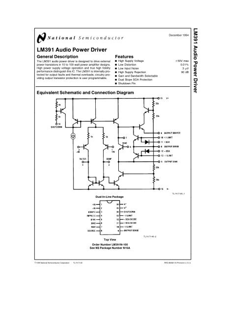
Equivalent Schematic and Connection Diagram<br />
December 1994<br />
Y High Supply Voltage g50V max<br />
Y Low Distortion 001%<br />
Y Low Input Noise 3 mV<br />
Y High Supply Rejection 90 dB<br />
Y<br />
Y<br />
Y<br />
Gain and Bandwidth Selectable<br />
Dual Slope SOA Protection<br />
Shutdown Pin<br />
<strong>LM391</strong> <strong>Audio</strong> <strong>Power</strong> <strong>Driver</strong><br />
Dual-In-Line Package<br />
TLH7146–1<br />
Top View<br />
Order Number <strong>LM391</strong>N-100<br />
See NS Package Number N16A<br />
TLH7146–2<br />
C1995 National Semiconductor Corporation<br />
TLH7146<br />
RRD-B30M115Printed in U S A
Absolute Maximum Ratings<br />
If MilitaryAerospace specified devices are required<br />
please contact the National Semiconductor Sales<br />
OfficeDistributors for availability and specifications<br />
Supply Voltage<br />
<strong>LM391</strong>N-100<br />
Input Voltage<br />
Shutdown Current (Pin 14)<br />
g50V or a100V<br />
Supply Voltage less 5V<br />
1 mA<br />
Package Dissipation (Note 1)<br />
Storage Temperature<br />
Operating Temperature<br />
Lead Temp (Soldering 10 sec)<br />
Thermal Resistance<br />
i JC<br />
i JA<br />
139W<br />
b65Ctoa150C<br />
0Ctoa70C<br />
260C<br />
20CW<br />
63CW<br />
Electrical Characteristics T A e 25C (The following are for V a e 90% V a MAX and V b e 90% V b MAX)<br />
Parameter Conditions Min Typ Max Units<br />
Quiescent Current Current in Pin 15<br />
mA<br />
<strong>LM391</strong>N-100 V IN e 0 5 6<br />
Output Swing Positive V a b 7 V a b 5 V<br />
Negative V b a 7 V b a 5 V<br />
Drive Current Source (Pin 8) 5 mA<br />
Sink (Pin 5) 5 mA<br />
Noise (20 Hz–20 kHz) Input Referred 3 mV<br />
Supply Rejection Input Referred 70 90 dB<br />
Total Harmonic Distortion f e 1 kHz 001 %<br />
f e 20 kHz 010 025 %<br />
Intermodulation Distortion 60 Hz 7 kHz 41 001 %<br />
Open Loop Gain f e 1 kHz 1000 5500 VV<br />
Input Bias Current 01 10 mA<br />
Input Offset Voltage 5 20 mV<br />
Positive Current Limit V BE Pin 10–9 650 mV<br />
Negative Current Limit V BE Pin 9–13 650 mV<br />
Positive Current Limit Bias Current Pin 10 10 100 mA<br />
Negative Current Limit Bias Current Pin 13 10 100 mA<br />
Pin 14 Current Comments<br />
Minimum pin 14 current required for shutdown is 05 mA and must not exceed 1 mA<br />
Maximum pin 14 current for amplifier not shut down is 005 mA<br />
The typical shutdown switch point current is 02 mA<br />
Note 1 For operation in ambient temperatures above 25C the device must be derated based on a 150C maximum junction temperature and a thermal resistance<br />
of 90CW junction to ambient<br />
Typical Applications<br />
FIGURE 1 <strong>LM391</strong> with External ComponentsProtection Circuitry Not Shown<br />
TLH7146–3<br />
2
Typical Performance Characteristics<br />
Total Harmonic Distortion vs<br />
Output <strong>Power</strong> vs Supply Voltage Frequency (R L e 8X)<br />
Total Harmonic Distortion vs<br />
Frequency (R L e 4X)<br />
Open Loop Gain vs Frequency<br />
Input Referred <strong>Power</strong> Supply<br />
Rejection vs Frequency<br />
Total Harmonic Distortion vs<br />
AB Bias Current<br />
Pin Descriptions<br />
TLH7146–4<br />
Pin No Pin Name Comments<br />
1 aInput <strong>Audio</strong> input<br />
2 bInput Feedback input<br />
3 Compensation Sets the dominant pole<br />
4 Ripple Filter Improves negative supply rejection<br />
5 Sink Output Drives output devices and is emitter of AB bias V BE multiplier<br />
6 BIAS Base of V BE multiplier<br />
7 BIAS Collector of V BE multiplier<br />
8 Source Output Drives output devices<br />
9 Output Sense Biases the IC and is used in protection circuits<br />
10 aCurrent Limit Base of positive side protection circuit transistor<br />
11 aSOA Diode Diode used for dual slope SOA protection<br />
12 bSOA Diode Diode used for dual slope SOA protection<br />
13 bCurrent Limit Base of negative side protection circuit transistor<br />
14 Shutdown Shuts off amplifier when current is pulled out of pin<br />
15 V a Positive supply<br />
16 V b Negative supply<br />
3
External Components (Figure 1)<br />
Component Typical Value Comments<br />
C IN 1 mF Input coupling capacitor sets a low frequency pole with R IN <br />
1<br />
f L e<br />
2qR IN C IN<br />
R IN 100k Sets input impedance and DC bias to input<br />
R f2 100k Feedback resistor for minimum offset voltage at the output this should be equal to R IN <br />
R f1 51k Feedback resistor that works with R f2 to set the voltage gain<br />
A V e 1 a R f 2<br />
R f1<br />
C f 10 mF Feedback capacitor This reduces the gain to unity at DC for minimum offset voltage at the<br />
output Also sets a low frequency pole with R f1 <br />
1<br />
f L e<br />
2qR f1 C f<br />
C C 5 pF Compensation capacitor Sets gain bandwidth product and a high frequency pole<br />
1<br />
GBW e<br />
f h e GBW<br />
2q5000C C A V<br />
Max f h for stable design 500 kHz<br />
R A 39k AB bias resistor<br />
R B 10k AB bias potentiometer Adjust to set bias current in the output stage<br />
C AB 01 mF Bypass capacitor for bias This improves high frequency distortion and transient response<br />
C R 5 pF Ripple capacitor This improves negative supply rejection at midband and high frequencies<br />
C R if used must equal C C <br />
R eb 100X Bleed resistor This removes stored charge in output transistors<br />
R O 27X Output compensation resistor This resistor and C O compensate the output stage This value<br />
will vary slightly for different output devices<br />
C O 01 mF Output compensation capacitor This works with R O to form a zero that cancels f b of the<br />
output power transistors<br />
R E 03X Emitter degeneration resistor This resistor gives thermal stability to the output stage<br />
quiescent current IRC PW5 type<br />
R TH 39k Shutdown resistor Sets the amount of current pulled out of pin 14 during shutdown<br />
C 2 C 2 1000 pF Compensation capacitors for protection circuitry<br />
X L 10Xll5 mH Used to isolate capacitive loads usually 20 turns of wire wrapped around a 10X 2W resistor<br />
4
Application Hints<br />
GENERALIZED AUDIO POWER AMP DESIGN<br />
Givens <strong>Power</strong> Output<br />
Load Impedance<br />
Input Sensitivity<br />
Input Impedance<br />
Bandwidth<br />
The power output and load impedance determine the power<br />
supply requirements Output signal swing and current are<br />
found from<br />
V Opeak e 02R L P O<br />
(1)<br />
I Opeak e<br />
0 2P O<br />
(2)<br />
R L<br />
Add 5 volts to the peak output swing (V OP ) for transistor<br />
voltage to get the supplies ie g (V OP a 5V) at a current<br />
of I peak The regulation of the supply determines the unloaded<br />
voltage usually about 15% higher Supply voltage will<br />
also rise 10% during high line conditions<br />
max supplies g(V Opeak a 5) (1 a regulation) (11) (3)<br />
The input sensitivity and output power specs determine the<br />
required gain<br />
A V<br />
t 0P O R L<br />
e V ORMS<br />
(4)<br />
V IN V INRMS<br />
Normally the gain is set between 20 and 200 for a 25 watt<br />
8 ohm amplifier this results in a sensitivity of 710 mV and 71<br />
mV respectively The higher the gain the higher the THD<br />
as can be seen from the characteristics curves Higher gain<br />
also results in more hum and noise at the output<br />
The desired input impedance is set by R IN Very high values<br />
can cause board layout problems and DC offsets at the output<br />
The bandwidth requirements determine the size of C f<br />
and C C as indicated in the external component listing<br />
The output transistors and drivers must have a breakdown<br />
voltage greater than the voltage determined by equation (3)<br />
The current gain of the drive and output device must be high<br />
enough to supply I Opeak with 5 mA of drive from the <strong>LM391</strong><br />
The power transistors must be able to dissipate approximately<br />
40% of the maximum output power the drivers must<br />
dissipate this amount divided by the current gain of the outputs<br />
See the output transistor selection guide Table A<br />
To prevent thermal runaway of the AB bias current the following<br />
equation must be valid<br />
i JA<br />
s R E (b MIN a 1)<br />
(5)<br />
V CEQMAX (K)<br />
where<br />
i JA is the thermal resistance of the driver transistor junction<br />
to ambient in CW<br />
R E is the emitter degeneration resistance in ohms<br />
b min is that of the output transistor<br />
V CEQMAX is the highest possible value of one supply from<br />
equation (3)<br />
K is the temperature coefficient of the driver base-emitter<br />
voltage typically 2 mVC<br />
Often the value of R E is to be determined and equation (5)<br />
is rearranged to be<br />
R E<br />
t i JA (V CEQMAX )K<br />
(6)<br />
b MIN a 1<br />
The maximum average power dissipation in each output<br />
transistor is<br />
P DMAX e 04 P OMAX<br />
(7)<br />
The power dissipation in the driver transistor is<br />
P DRIVER(MAX) e P DMAX<br />
(8)<br />
b MIN<br />
Heat sink requirements are found using the following formulas<br />
i JA<br />
s T JMAX b T AMAX<br />
(9)<br />
P D<br />
i SA<br />
s i JA b i JC b i CS<br />
(10)<br />
where<br />
T jMAX is the maximum transistor junction temperature<br />
T AMAX is the maximum ambient temperature<br />
i JA is thermal resistance junction to ambient<br />
i SA is thermal resistance sink to ambient<br />
i JC is thermal resistance junction to case<br />
i CS is thermal resistance case to sink typically 1CW for<br />
most mountings<br />
5
Application Hints (Continued)<br />
PROTECTION CIRCUITRY<br />
The protection circuits of the <strong>LM391</strong> are very flexible and<br />
should be tailored to the output transistor’s safe operating<br />
area The protection V-I characteristics circuitry and resistor<br />
formulas are described below The diodes from the output<br />
to each supply prevent the output voltage from exceeding<br />
the supplies and harming the output transistors The output<br />
will do this if the protection circuitry is activated while<br />
driving an inductive load<br />
TURN-ON DELAY<br />
It is often desirable to delay the turn-ON of the power amplifier<br />
This is easily implemented by putting a resistor in series<br />
with a capacitor from pin 14 to ground The value of the<br />
Protection Circuitry with External Components<br />
resistor is set to limit the current to less than 1 mA (the<br />
absolute maximum) This resistor with the capacitor gives a<br />
time constant of RC The turn-ON delay is approximately 2<br />
time constants<br />
Example<br />
Amplifier with maximum supply of 30V like the 20W 8X<br />
example in the data sheet requiring a delay of 1 second<br />
Time delay e 2RC<br />
Max Va<br />
Re<br />
1mA<br />
So<br />
R e 30k Solving for C gives 167 mF Use C e 20 mF with<br />
a 30V rating<br />
Protection Characteristics<br />
TLH7146–6<br />
TLH7146–5<br />
Protection Circuit Resistor Formulas (V B e V a )<br />
Type of Protection R E R R 1 R 1 R 2 R 2 R 3 R 3<br />
Current Limit R E e w I L<br />
Not Required Short Not Required<br />
Single Slope SOA<br />
Protection<br />
R E e w I L<br />
Dual Slope SOA<br />
Protection R E e w R 1 e R 2<br />
I L V M b w<br />
(V B e V a )<br />
R 1 e R 2<br />
V M b w<br />
w J<br />
1kX Not Required<br />
w J<br />
1kX R 3 eR 2<br />
<br />
V a<br />
I LR E bw b1 (<br />
Note w is the current limit V BE voltage 650 mV Assumptions V a ll wV M ll wVa is the load supply voltage V M is the maximum rated V CE of the output<br />
transistors<br />
6
Application Hints (Continued)<br />
TRANSIENT INTERMODULATION DISTORTION<br />
There has been a lot of interest in recent years about transient<br />
intermodulation distortion Matti Otala of University of<br />
Oulu Oulu Finland has published several papers on the<br />
subject The results of these investigations show that the<br />
open loop pole of the power amplifier should be above 20<br />
kHz<br />
To do this with the <strong>LM391</strong> is easy Put a1MXresistor from<br />
pin 3 to the output and the open loop gain is reduced to<br />
about 46 dB Now the open loop pole is at 30 kHz The<br />
current in this resistor causes an offset in the input stage<br />
that can be cancelled with a resistor from pin 4 to ground<br />
The resistor from pin 4 to ground should be 910 kX rather<br />
than 1 MX to insure that the shutdown circuitry will operate<br />
correctly The slight difference in resistors results in about<br />
15 mV of offset The 40W 8X amplifier schematic shows<br />
the hookup of these two resistors<br />
BRIDGE AMPLIFIER<br />
A switch can be added to convert a stereo amplifer to a<br />
single bridge amplifer The diagram below shows where the<br />
switch and one resistor are added When operating in the<br />
bridge mode the output load is connected between the two<br />
outputs the input is V IN 1 and V IN 2 is disconnected<br />
OSCILLATIONS GROUNDING<br />
Most power amplifiers work the first time they are turned on<br />
They also tend to oscillate and have excess THD Most oscillation<br />
problems are due to inadequate supply bypassing<br />
andor ground loops A 10 mF 50V electrolytic on each<br />
power supply will stop supply-related oscillations However<br />
if the signal ground is used for these bypass caps the THD<br />
is usually excessive The signal ground must return to the<br />
power supply alone as must the output load ground All<br />
other groundsbypass output R-C protection etc can tie<br />
together and then return to supply This ground is called<br />
high frequency ground On the 40W amplifier schematic all<br />
the grounds are labeled<br />
Capacitive loads can cause instabilities so they are isolated<br />
from the amplifier with an inductor and resistor in the output<br />
lead<br />
AB BIAS CURRENT<br />
To reduce distortion in the output stage all the transistors<br />
are biased ON slightly This results in class AB operation<br />
and reduces the crossover (notch) distortion of the class B<br />
stage to a low level (see performance curve THD vs AB<br />
bias) The potentiometer R B from pins 6–7 is adjusted to<br />
give about 25 mA of current in the output stage This current<br />
is usually monitored at the supply or by measuring the voltage<br />
across R E <br />
Typical Applications (Continued)<br />
Bridge Circuit Diagram<br />
Output Transistors Selection Guide<br />
Table A<br />
<strong>Power</strong> <strong>Driver</strong> Transistor Output Transistor<br />
Output PNP NPN PNP NPN<br />
20W 8X MJE711 MJE721 TIP42A TIP41A<br />
30W 4X MJE171 MJE181 2N6490 2N6487<br />
D43C8<br />
D42C8<br />
40W 8X MJE712 MJE722 2N5882 2N5880<br />
60W 4X MJE172 MJE182<br />
D43C11<br />
D42C11<br />
TLH7146–7<br />
7
Application Hints (Continued)<br />
A 20W 8X 30W 4X AMPLIFIER<br />
Givens<br />
<strong>Power</strong> Output<br />
20W into 8X<br />
30W into 4X<br />
1V Max<br />
100k<br />
20 Hz–20 kHz g 025 dB<br />
Input Sensitivity<br />
Input Impedance<br />
Bandwidth<br />
Equations (1) and (2) give<br />
20W8X V OP e 179V I OP e 224A<br />
30W4X V OP e 155V I OP e 387A<br />
Therefore the supply required is<br />
g23V 224A reducing to <br />
g21V 387A<br />
With 15% regulation and high line we get g29V from equation<br />
(3)<br />
Sensitivity and equation (4) set minimum gain<br />
A V<br />
t 020 c 8 e 1265<br />
1<br />
We will use a gain of 20 with resulting sensitivity of 632 mV<br />
Letting R IN equal 100k gives the required input impedance<br />
For low DC offsets at the output we let R f2 e 100k Solving<br />
for R f1 gives<br />
R f2 e 100k<br />
R f1 e<br />
100k e 526k use 51k<br />
20 b 1<br />
The bandwidth requirement must be stated as a pole ie<br />
the 3 dB frequency Five times away from a pole gives 017<br />
dB down which is better than the required 025 dB Therefore<br />
f L e 20 5 e 4Hz<br />
Solving for C f <br />
1<br />
C f<br />
t e 78 mF use 10 mF<br />
2qR f1 f L<br />
The recommended value for C C is 5 pF for gains of 20 or<br />
larger This gives a gain-bandwidth product of 64 MHz and<br />
a resulting bandwidth of 320 kHz better than required<br />
The breakdown voltage requirement is set by the maximum<br />
supply we need a minimum of 58V and will use 60V We<br />
must now select a 60V power transistor with reasonable<br />
beta at I Opeak 387A The TIP42 TIP41 complementary pair<br />
are 60V 60W transistors with a minimum beta of 30 at 4A<br />
The driver transistor must supply the base drive given 5 mA<br />
drive from the <strong>LM391</strong> The MJE711 MJE721 complementary<br />
driver transistors are 60V devices with a minimum beta of<br />
40 at 200 mA The driver transistors should be much faster<br />
(higher f T ) than the output transistors to insure that the R-C<br />
on the output will prevent instability<br />
To find the heat sink required for each output transistor we<br />
use equations (7) (9) and (10)<br />
P D e 04 (30) e 12W<br />
(7)<br />
150C b 55C<br />
i JA<br />
s e 79CW for T AMAX e 55C (9)<br />
12<br />
i SA<br />
s 79 b 21 b 10 e 48CW (10)<br />
If both transistors are mounted on one heat sink the thermal<br />
resistance should be halved to 24CW<br />
The maximum average power dissipation in each driver is<br />
found using equation (8)<br />
P DRIVER(MAX) e 12 e 400 mW<br />
30<br />
Using equation (9)<br />
155 b 55<br />
i JA<br />
s e 237CW<br />
04<br />
f h e20k c 5 e 100 kHz<br />
8
Application Hints (Continued)<br />
Since the free air thermal resistance of the MJE711<br />
MJE721 is 100CW no heat sink is required Using this<br />
information and equation (6) we can find the minimum value<br />
of R E required to prevent thermal runaway<br />
100 (30) (0002)<br />
R E<br />
t e 019X (6)<br />
30 a 1<br />
We must now use the SOA data on the TIP42 TIP41 transistors<br />
to set up the protection circuit Below is the SOA<br />
curve with the 4X and 8X load lines Also shown are the<br />
desired protection lines Note the value of V B is equal to the<br />
supply voltage so we use the formulas in the table<br />
DC SOA of TIP42 TIP41<br />
Transistors<br />
The data points from the curve are<br />
V M e 60V V B e 23V I L e 3A I L e 7A<br />
Using the dual slope protection formulas<br />
R E e 065<br />
3 e 022X<br />
R 2 e 1k<br />
60 b 065<br />
R 1 e 1k<br />
065 J 91k<br />
23<br />
R 3 e 1k<br />
7(022) b 065 b 1 J 24k<br />
Note that an R E of 022X satisfies equation (6) The final<br />
schematic of this amplifier is below If the output is shorted<br />
the current will be 18A and V CE is 23V Since the input is<br />
AC the average power is<br />
short P D e (18) (23) 21W<br />
This power is greater than was used in the heat sink calculations<br />
so the transistors will overheat for long-duration<br />
shorts unless a larger heat sink is used<br />
TLH7146–8<br />
Typical Applications (Continued)<br />
20W-8X 30W-4X Amplifier with 1 Second Turn-ON Delay<br />
Additional protection for <strong>LM391</strong>N Schottky diodes and R j 100X<br />
TLH7146–9<br />
9
Application Hints (Continued)<br />
A 40W8X 60W4X AMPLIFIER<br />
Given<br />
<strong>Power</strong> Output<br />
40W8X<br />
60W4X<br />
1V Max<br />
100k<br />
20 Hz–20 kHz g 025 dB<br />
Input Sensitivity<br />
Input Impedance<br />
Bandwidth<br />
Equations (1) and (2) give<br />
40W8X V OPeak e 253V I OPeak e 316A<br />
60W4X V OPeak e 219V I OPeak e 548A<br />
Therefore the supply required is<br />
g303V 316A reducing to <br />
g269V 548A<br />
With 15% regulation and high line we get g383V using<br />
equation (3)<br />
The minimum gain from equation (4) is<br />
A V<br />
t 18<br />
We select a gain of 20 resulting sensitivity is 900 mV<br />
The input impedance and bandwidth are the same as the 20<br />
watt amplifier so the components are the same<br />
R f1 e 51k R IN e 100k C C e 5pF<br />
R f2 e100k C f e 10 mF<br />
The maximum supplies dictate using 80V devices The<br />
2N5882 2N5880 pair are 80V 160W transistors with a minimum<br />
beta of 40 at 2A and 20 at 6A This corresponds to a<br />
minimum beta of 225 at 55A (I Opeak ) The MJE712<br />
MJE722 driver pair are 80V transistors with a minimum beta<br />
of 50 at 250 mA This output combination guarantees I Opeak<br />
with 5 mA from the <strong>LM391</strong><br />
Output transistor heat sink requirements are found using<br />
equations (7) (9) and (10)<br />
P D e 04 (60) e 24W<br />
(7)<br />
200 b 55<br />
i JA<br />
s e 60CW for T AMAX e 55C (9)<br />
24<br />
i SA<br />
s 60 b 11 b 10 e 39CW (10)<br />
For both output transistors on one heat sink the thermal<br />
resistance should be 19CW<br />
Now using equation (8) we find the power dissipation in the<br />
driver<br />
P DRIVER e 24 e 12W (8)<br />
20<br />
150 b 55<br />
i JA<br />
s e 79CW (9)<br />
12<br />
Since a heat sink is required on the driver we should investigate<br />
the output stage thermal stability at the same time to<br />
optimize the design If we find a value of R E that is good for<br />
the protection circuitry we can then use equation (5) to find<br />
the heat sink required for the drivers<br />
The SOA characteristics of the 2N5882 2N5880 transistors<br />
are shown in the following curve along with a desired protection<br />
line<br />
SOA 2N5882 2N5880<br />
TLH7146–10<br />
The desired data points are<br />
V M e 80V V B e 47V I L e 3A I L e 11A<br />
Since the break voltage is not equal to the supply we will<br />
use two resistors to replace R 3 and move V B <br />
Circuit Used<br />
Thevenin Equivalent<br />
TLH7146–11<br />
Where R TH e R A 3 ll R B 3<br />
V TH e V b R<br />
<br />
A 3<br />
R A 3 3( a RB<br />
TLH7146–12<br />
10
Application Hints (Continued)<br />
The formulas for R E R 1 and R 2 do not change<br />
R E e 065<br />
3A e 022X<br />
80 b 065<br />
R 2 e 1k R 1 e 1k e 120k<br />
065<br />
The formula for R 3 now gives R TH when the V a in the formula<br />
becomes V B <br />
V<br />
R TH e B<br />
R 2<br />
I L R E b w b 1 (<br />
47<br />
e 1k<br />
11 (022) b 065 b 1 ( e 2555k<br />
V TH is the additional voltage added to the supply voltage to<br />
get V B <br />
V TH eb(V B b V a ) eb(47 b 30) eb17V<br />
Now we must find R A 3 and R B 3 using the Thevenin formulas<br />
Putting V TH V b and R TH into the appropriate formulas reduces<br />
to<br />
R B 3 e 076 RA 3 and 2555k e R A 3 ll R B 3<br />
The easiest way to solve these equations is to iterate with<br />
standard values If we guess R A 3 e 62k then RB 3 e 4712k<br />
use 47k The Thevenin impedance comes out 267k which<br />
is close enough to 2555k<br />
Now we will use equation (5) to determine the heat sinking<br />
requirements of the drivers to insure thermal stability<br />
022 (20 a 1)<br />
i JA<br />
s 57CW (5)<br />
40 (0002)<br />
This value is lower than we got with equation (9) so we will<br />
use it in equation (10)<br />
i SA<br />
s 57 b 6 b 1 e 50CW (10)<br />
This is the required heat sink for each driver For low TIM<br />
we add the 1 MX resistor from pin 3 to the output and a<br />
910k resistor from pin 4 to ground The complete schematic<br />
is shown below<br />
If the output is shorted the transistor voltage is about 28V<br />
and the current is 5A Therefore the average power is<br />
short PD e (28) 5 e 70W<br />
This is much larger than the power used to calculate the<br />
heat sinks and the output transistors will overheat if the output<br />
is shorted too long<br />
Typical Applications (Continued)<br />
40W-8X 60W-4X Amplifier<br />
High Frequency Ground<br />
Input Ground<br />
Speaker Ground<br />
Note All Grounds Should be Tied Together<br />
Only at <strong>Power</strong> Supply Ground<br />
Additional protection for <strong>LM391</strong>N Schottky diodes and R j 100X<br />
TLH7146–13<br />
11
<strong>LM391</strong> <strong>Audio</strong> <strong>Power</strong> <strong>Driver</strong><br />
Physical Dimensions inches (millimeters)<br />
Molded Dual-In-Line Package (N)<br />
Order Number <strong>LM391</strong>N-100<br />
NS Package Number N16A<br />
LIFE SUPPORT POLICY<br />
NATIONAL’S PRODUCTS ARE NOT AUTHORIZED FOR USE AS CRITICAL COMPONENTS IN LIFE SUPPORT<br />
DEVICES OR SYSTEMS WITHOUT THE EXPRESS WRITTEN APPROVAL OF THE PRESIDENT OF NATIONAL<br />
SEMICONDUCTOR CORPORATION As used herein<br />
1 Life support devices or systems are devices or 2 A critical component is any component of a life<br />
systems which (a) are intended for surgical implant support device or system whose failure to perform can<br />
into the body or (b) support or sustain life and whose be reasonably expected to cause the failure of the life<br />
failure to perform when properly used in accordance support device or system or to affect its safety or<br />
with instructions for use provided in the labeling can effectiveness<br />
be reasonably expected to result in a significant injury<br />
to the user<br />
National Semiconductor National Semiconductor National Semiconductor National Semiconductor<br />
Corporation Europe Hong Kong Ltd Japan Ltd<br />
1111 West Bardin Road Fax (a49) 0-180-530 85 86 13th Floor Straight Block Tel 81-043-299-2309<br />
Arlington TX 76017 Email cnjwge tevm2nsccom Ocean Centre 5 Canton Rd Fax 81-043-299-2408<br />
Tel 1(800) 272-9959 Deutsch Tel (a49) 0-180-530 85 85 Tsimshatsui Kowloon<br />
Fax 1(800) 737-7018 English Tel (a49) 0-180-532 78 32 Hong Kong<br />
Franais Tel (a49) 0-180-532 93 58 Tel (852) 2737-1600<br />
Italiano Tel (a49) 0-180-534 16 80 Fax (852) 2736-9960<br />
National does not assume any responsibility for use of any circuitry described no circuit patent licenses are implied and National reserves the right at any time without notice to change said circuitry and specifications


