

LM391 Audio Power Driver
LM391 Audio Power Driver
LM391 Audio Power Driver

You also want an ePaper? Increase the reach of your titles
YUMPU automatically turns print PDFs into web optimized ePapers that Google loves.
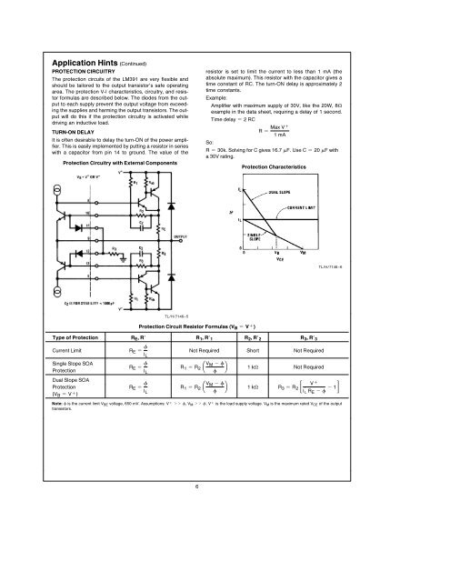
Application Hints (Continued)<br />
PROTECTION CIRCUITRY<br />
The protection circuits of the <strong>LM391</strong> are very flexible and<br />
should be tailored to the output transistor’s safe operating<br />
area The protection V-I characteristics circuitry and resistor<br />
formulas are described below The diodes from the output<br />
to each supply prevent the output voltage from exceeding<br />
the supplies and harming the output transistors The output<br />
will do this if the protection circuitry is activated while<br />
driving an inductive load<br />
TURN-ON DELAY<br />
It is often desirable to delay the turn-ON of the power amplifier<br />
This is easily implemented by putting a resistor in series<br />
with a capacitor from pin 14 to ground The value of the<br />
Protection Circuitry with External Components<br />
resistor is set to limit the current to less than 1 mA (the<br />
absolute maximum) This resistor with the capacitor gives a<br />
time constant of RC The turn-ON delay is approximately 2<br />
time constants<br />
Example<br />
Amplifier with maximum supply of 30V like the 20W 8X<br />
example in the data sheet requiring a delay of 1 second<br />
Time delay e 2RC<br />
Max Va<br />
Re<br />
1mA<br />
So<br />
R e 30k Solving for C gives 167 mF Use C e 20 mF with<br />
a 30V rating<br />
Protection Characteristics<br />
TLH7146–6<br />
TLH7146–5<br />
Protection Circuit Resistor Formulas (V B e V a )<br />
Type of Protection R E R R 1 R 1 R 2 R 2 R 3 R 3<br />
Current Limit R E e w I L<br />
Not Required Short Not Required<br />
Single Slope SOA<br />
Protection<br />
R E e w I L<br />
Dual Slope SOA<br />
Protection R E e w R 1 e R 2<br />
I L V M b w<br />
(V B e V a )<br />
R 1 e R 2<br />
V M b w<br />
w J<br />
1kX Not Required<br />
w J<br />
1kX R 3 eR 2<br />
<br />
V a<br />
I LR E bw b1 (<br />
Note w is the current limit V BE voltage 650 mV Assumptions V a ll wV M ll wVa is the load supply voltage V M is the maximum rated V CE of the output<br />
transistors<br />
6


