LM391 Audio Power Driver
LM391 Audio Power Driver
LM391 Audio Power Driver
You also want an ePaper? Increase the reach of your titles
YUMPU automatically turns print PDFs into web optimized ePapers that Google loves.
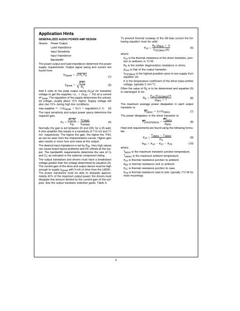
Application Hints<br />
GENERALIZED AUDIO POWER AMP DESIGN<br />
Givens <strong>Power</strong> Output<br />
Load Impedance<br />
Input Sensitivity<br />
Input Impedance<br />
Bandwidth<br />
The power output and load impedance determine the power<br />
supply requirements Output signal swing and current are<br />
found from<br />
V Opeak e 02R L P O<br />
(1)<br />
I Opeak e<br />
0 2P O<br />
(2)<br />
R L<br />
Add 5 volts to the peak output swing (V OP ) for transistor<br />
voltage to get the supplies ie g (V OP a 5V) at a current<br />
of I peak The regulation of the supply determines the unloaded<br />
voltage usually about 15% higher Supply voltage will<br />
also rise 10% during high line conditions<br />
max supplies g(V Opeak a 5) (1 a regulation) (11) (3)<br />
The input sensitivity and output power specs determine the<br />
required gain<br />
A V<br />
t 0P O R L<br />
e V ORMS<br />
(4)<br />
V IN V INRMS<br />
Normally the gain is set between 20 and 200 for a 25 watt<br />
8 ohm amplifier this results in a sensitivity of 710 mV and 71<br />
mV respectively The higher the gain the higher the THD<br />
as can be seen from the characteristics curves Higher gain<br />
also results in more hum and noise at the output<br />
The desired input impedance is set by R IN Very high values<br />
can cause board layout problems and DC offsets at the output<br />
The bandwidth requirements determine the size of C f<br />
and C C as indicated in the external component listing<br />
The output transistors and drivers must have a breakdown<br />
voltage greater than the voltage determined by equation (3)<br />
The current gain of the drive and output device must be high<br />
enough to supply I Opeak with 5 mA of drive from the <strong>LM391</strong><br />
The power transistors must be able to dissipate approximately<br />
40% of the maximum output power the drivers must<br />
dissipate this amount divided by the current gain of the outputs<br />
See the output transistor selection guide Table A<br />
To prevent thermal runaway of the AB bias current the following<br />
equation must be valid<br />
i JA<br />
s R E (b MIN a 1)<br />
(5)<br />
V CEQMAX (K)<br />
where<br />
i JA is the thermal resistance of the driver transistor junction<br />
to ambient in CW<br />
R E is the emitter degeneration resistance in ohms<br />
b min is that of the output transistor<br />
V CEQMAX is the highest possible value of one supply from<br />
equation (3)<br />
K is the temperature coefficient of the driver base-emitter<br />
voltage typically 2 mVC<br />
Often the value of R E is to be determined and equation (5)<br />
is rearranged to be<br />
R E<br />
t i JA (V CEQMAX )K<br />
(6)<br />
b MIN a 1<br />
The maximum average power dissipation in each output<br />
transistor is<br />
P DMAX e 04 P OMAX<br />
(7)<br />
The power dissipation in the driver transistor is<br />
P DRIVER(MAX) e P DMAX<br />
(8)<br />
b MIN<br />
Heat sink requirements are found using the following formulas<br />
i JA<br />
s T JMAX b T AMAX<br />
(9)<br />
P D<br />
i SA<br />
s i JA b i JC b i CS<br />
(10)<br />
where<br />
T jMAX is the maximum transistor junction temperature<br />
T AMAX is the maximum ambient temperature<br />
i JA is thermal resistance junction to ambient<br />
i SA is thermal resistance sink to ambient<br />
i JC is thermal resistance junction to case<br />
i CS is thermal resistance case to sink typically 1CW for<br />
most mountings<br />
5


