

LM391 Audio Power Driver
LM391 Audio Power Driver
LM391 Audio Power Driver

Create successful ePaper yourself
Turn your PDF publications into a flip-book with our unique Google optimized e-Paper software.
Application Hints (Continued)<br />
TRANSIENT INTERMODULATION DISTORTION<br />
There has been a lot of interest in recent years about transient<br />
intermodulation distortion Matti Otala of University of<br />
Oulu Oulu Finland has published several papers on the<br />
subject The results of these investigations show that the<br />
open loop pole of the power amplifier should be above 20<br />
kHz<br />
To do this with the <strong>LM391</strong> is easy Put a1MXresistor from<br />
pin 3 to the output and the open loop gain is reduced to<br />
about 46 dB Now the open loop pole is at 30 kHz The<br />
current in this resistor causes an offset in the input stage<br />
that can be cancelled with a resistor from pin 4 to ground<br />
The resistor from pin 4 to ground should be 910 kX rather<br />
than 1 MX to insure that the shutdown circuitry will operate<br />
correctly The slight difference in resistors results in about<br />
15 mV of offset The 40W 8X amplifier schematic shows<br />
the hookup of these two resistors<br />
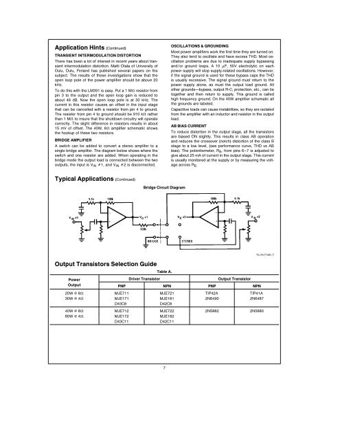
BRIDGE AMPLIFIER<br />
A switch can be added to convert a stereo amplifer to a<br />
single bridge amplifer The diagram below shows where the<br />
switch and one resistor are added When operating in the<br />
bridge mode the output load is connected between the two<br />
outputs the input is V IN 1 and V IN 2 is disconnected<br />
OSCILLATIONS GROUNDING<br />
Most power amplifiers work the first time they are turned on<br />
They also tend to oscillate and have excess THD Most oscillation<br />
problems are due to inadequate supply bypassing<br />
andor ground loops A 10 mF 50V electrolytic on each<br />
power supply will stop supply-related oscillations However<br />
if the signal ground is used for these bypass caps the THD<br />
is usually excessive The signal ground must return to the<br />
power supply alone as must the output load ground All<br />
other groundsbypass output R-C protection etc can tie<br />
together and then return to supply This ground is called<br />
high frequency ground On the 40W amplifier schematic all<br />
the grounds are labeled<br />
Capacitive loads can cause instabilities so they are isolated<br />
from the amplifier with an inductor and resistor in the output<br />
lead<br />
AB BIAS CURRENT<br />
To reduce distortion in the output stage all the transistors<br />
are biased ON slightly This results in class AB operation<br />
and reduces the crossover (notch) distortion of the class B<br />
stage to a low level (see performance curve THD vs AB<br />
bias) The potentiometer R B from pins 6–7 is adjusted to<br />
give about 25 mA of current in the output stage This current<br />
is usually monitored at the supply or by measuring the voltage<br />
across R E <br />
Typical Applications (Continued)<br />
Bridge Circuit Diagram<br />
Output Transistors Selection Guide<br />
Table A<br />
<strong>Power</strong> <strong>Driver</strong> Transistor Output Transistor<br />
Output PNP NPN PNP NPN<br />
20W 8X MJE711 MJE721 TIP42A TIP41A<br />
30W 4X MJE171 MJE181 2N6490 2N6487<br />
D43C8<br />
D42C8<br />
40W 8X MJE712 MJE722 2N5882 2N5880<br />
60W 4X MJE172 MJE182<br />
D43C11<br />
D42C11<br />
TLH7146–7<br />
7


