

May 2013 - I-Micronews
May 2013 - I-Micronews
May 2013 - I-Micronews

Create successful ePaper yourself
Turn your PDF publications into a flip-book with our unique Google optimized e-Paper software.
3D<br />
ISSUE N°27<br />
MAY <strong>2013</strong><br />
Packaging<br />
Magazine on 3DIC, TSV, WLP & Embedded Die Technologies<br />
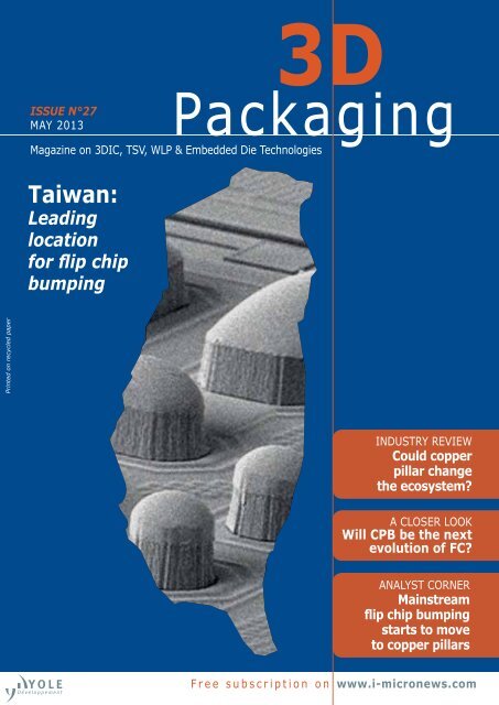
Taiwan:<br />
Leading<br />
location<br />
for flip chip<br />
bumping<br />
Printed on recycled paper<br />
Industry review<br />
Could copper<br />
pillar change<br />
the ecosystem?<br />
A CLOSER LOOK<br />
Will CPB be the next<br />
evolution of FC?<br />
analyst corner<br />
Mainstream<br />
flip chip bumping<br />
starts to move<br />
to copper pillars<br />
Free subscription on www.i-micronews.com
Watch the Editorial Webcast<br />
Archive on Flip Chip<br />
on i-<strong>Micronews</strong>.com<br />
Need an updated in-depth<br />
understanding of flip-chip<br />
technologies?<br />
What’s new compared to last edition?<br />
• A new top-down approach, leading to an exhaustive<br />
quantification of IC using Flip-Chip<br />
• Micro-bumping and accurate modeling of memory<br />
and HB-LED applications<br />
• Market data for TIM, underfills, substrates and<br />
Flip-Chip bonders<br />
• Detailed technology roadmap<br />
Flip Chip<br />
Discover the NEW report on<br />
www.i-<strong>Micronews</strong>.com/reports
M A Y 2 0 1 3 I S S U E N ° 2 7<br />
E D I T O R I A L<br />
An established platform rescues most<br />
advanced silicon technologies<br />
Dear 3D Packaging readers,<br />
It’s my pleasure to share with you our outlook for the fantastic, long-lasting<br />
potential of a proven Advanced Packaging technology: flip chip.<br />
No doubt you’re wondering why the spotlight is now being shone on this<br />
long-established technology. There are several reasons, two of which are<br />
value and technology. Technology equates to the customer’s perception<br />
of a product’s advantages, be they features, performance or reliability.<br />
Of the three, performance has always been the key decision-making<br />
parameter for consumers, because each new device generation brings<br />
significant speed improvements like calculation, graphical display or data<br />
transfer time. Performance improvement is the outcome of mainstream<br />
semiconductor technology’s node change, and it always carries large<br />
...the opening of<br />
interconnection between<br />
heterogeneous<br />
chips in the same package,<br />
flip chip is the ideal path...<br />
investments. Of course, return on investment is the driving force for<br />
most IC manufacturers -- but going from a 90nm technology node to 32<br />
and beyond requires an increased interconnect need that wire-bonding<br />
simply cannot match. So what could be the way out?<br />
Enter flip chip, which has resurfaced to rescue designers and solve the<br />
technological challenge of linking the sub-20 nanometer gate length to<br />
the millimeter world. With copper pillar pitch reduction allowing for wider<br />
I/O connectivity, and the opening of interconnection between heterogeneous<br />
chips in the same package, flip chip is the ideal path. Moreover,<br />
any Advanced Packaging scheme ends with bumping opening the<br />
door to very large adoption.<br />
Regarding value, flip chip offers the outstanding benefit of being realized<br />
at wafer level, thus significantly reducing manufacturing cost compared<br />
e v e n t s<br />
• Electronic Components and Technology<br />
Conference (ECTC)<br />
<strong>May</strong> 28 to 31, <strong>2013</strong> - Las Vegas, NV<br />
• SEMICON Russia<br />
June 5 to 6, <strong>2013</strong> - Moscow, Russia<br />
• SEMI Networking Day: Packaging - Key<br />
Driver for System Integration<br />
June 27, <strong>2013</strong> - Porto, Portugal<br />
to single chip wire bonding.<br />
I’m confident that by the end of this 3D Packaging issue, you’ll have a<br />
much better understanding of Flip chip’s technology, market and potential.<br />
Christophe Fitamant<br />
Sales & Marketing Director<br />
Yole Développement<br />
fitamant@yole.fr<br />
• SEMICON West<br />
July 9 to 11, <strong>2013</strong> - San Francisco, CA<br />
platinum partners:<br />
3 D P a c k a g i n g 3<br />
For more information, please contact S. Leroy (leroy@yole.fr)
M A Y 2 0 1 3 I S S U E N ° 2 7<br />
C O N T E N T S<br />
INDUSTRY REVIEW<br />
• Could copper pillar change the ecosystem? 6<br />
YOLE ASKS<br />
• Keeping up with the industry heavyweights 10<br />
A CLOSER LOOK<br />
• Will CPB be the next evolution of FC? 12<br />
(Courtesy of FlipChip<br />
International)<br />
• The evolution of Flip Chip packaging 14<br />
Analyst Corner<br />
• Mainstream flip chip bumping starts to move to copper pillars 16<br />
From i-<strong>Micronews</strong>.com<br />
Stay connected with your peers<br />
on i-<strong>Micronews</strong>.com<br />
With 20,000 monthly visitors,<br />
i-<strong>Micronews</strong>.com provides for Advanced<br />
Packaging area: current news, market<br />
& technological analysis, key leader<br />
interviews, webcasts section, reverse<br />
engineering / costing, events calendar,<br />
latest reports …<br />
Please visit our website to discover the<br />
last top stories in Advanced Packaging:<br />
> ASE to buy Toshiba backend plant in<br />
China<br />
> Silex joins ENIAC project to develop<br />
new solutions for TSV and wafer<br />
bonding<br />
> A Top 5 worldwide semiconductor<br />
vendor has qualified ALSI’s multibeam<br />
laser dicing system<br />
gold partners:<br />
4 3 D P a c k a g i n g
Watch it now<br />
Editorial Webcast available today<br />
<strong>2013</strong> PROGRAM:<br />
June 11<br />
Silicon Microfluidics:<br />
Myth or Reality?<br />
July 9<br />
IR imagers:<br />
How cost decrease<br />
will generate<br />
new markets<br />
Flip Chip: An established<br />
platform still in mutation...<br />
...And despite its longevity, Flip Chip is still able to<br />
serve the most advanced packaging technologies<br />
Hosted by:<br />
For more information and to register, please go to<br />
www.i-micronews.com/webcasts.asp or click here<br />
Powered by:
M A Y 2 0 1 3 I S S U E N ° 2 7<br />
INDUSTRY REVIEW<br />
Three quarter wafer<br />
Cu pillar bumps<br />
(Courtesy of<br />
Amkor Technology)<br />
Could copper pillar change<br />
the ecosystem?<br />
The future of bumping is copper, and that could change everything. Though originally<br />
developed at the IDMs, players from foundries to OSATs are now developing a variety<br />
of differing copper pillar and micro-bumping solutions for a range of customers,<br />
looking re-designing the substrate, weighing extending reflow vs scaling thermal<br />
compression bonding, and developing probe and test systems.<br />
Though copper bumping has been around for<br />
years, higher density devices mean growing<br />
demand for higher density interconnect<br />
than the ~130-140µm pitch that can be done with<br />
solder bumps. As mobile application or baseband<br />
processors increasingly require the high density of<br />
copper pillars for small size at 28nm and below, and<br />
memory soon starts to go to wide I/O and DDR4<br />
stacked with processors needing higher pin counts<br />
and reduced parasitics, manufacturers are focusing<br />
on scaling copper technology to tighter pitches,<br />
higher volumes, and of course lower costs.<br />
“For copper pillar bumping, the industry will have<br />
to solve similar challenges as it did for copper wire<br />
bonding—the materials are different, the substrates<br />
are different, and the designs are different. Moving<br />
beyond solder will require a whole new ecosystem,<br />
and will require working closely with our customers<br />
and with our materials and equipment partners,”<br />
says Bill Chen, ASE Fellow and Senior Technical<br />
Advisor.<br />
“Copper is a node change for bumping,” concurs David<br />
McCann, VP of Packaging R&D at GLOBALFOUNDRIES,<br />
pointing out that this node should be extendible more<br />
than the usual 7 years, all the way down through<br />
10µm pitch connections and below. “We see copper as<br />
a core competency for several generations,” he adds,<br />
noting that the company is investing significantly in<br />
people and projects to develop copper expertise,<br />
counting on the same core knowledge and tools to<br />
extend to beyond copper pillar and micro-bumping<br />
down to copper-to-copper bumpless bonding below<br />
14µm. GLOBALFOUNDRIES is developing Cu pillar<br />
technology in its Dresden facility and will be adding<br />
a bump facility, focusing on Cu pillar production at<br />
its Fab 8 facility in New York. The New York facility<br />
will enable interconnect and package R&D co-located<br />
with its front-end development teams for advanced<br />
nodes. Development in Dresden focuses on 100-<br />
110µm pitch bumps for 28nm, and 40µm/80µm<br />
pitch for 20nm.<br />
STATS ChipPAC is currently doing staggered<br />
40µm/80µm pitch Cu columns, with 20-30µm bumps<br />
on 80µm pitch centers for 28nm mobile processors,<br />
reports Raj Pendse, VP and Chief Marketing Officer.<br />
Similar technology should be extendible to 20nm<br />
processors, he suggests, as the relatively low I/O<br />
density of the power and ground in the center of<br />
the processor die means there will likely be enough<br />
room to just add more rows of the same 80µm pitch<br />
columns.<br />
6<br />
3 D P a c k a g i n g
I S S U E N ° 2 7<br />
M A Y 2 0 1 3<br />
a<br />
Foundries are also developing their own<br />
solutions with their customers. “Some<br />
foundries want to control the entire supply<br />
chain but we want to enable our customers’<br />
supply chain choices. We also need the fast<br />
feedback of probe results to the fab drive<br />
early yields,” says McCann. “But we don’t<br />
Pendse concurs that OSATs will take a larger<br />
role as the technology matures, as dividing<br />
responsibility for yield between the fab and<br />
OSAT when transferring bumped wafers will<br />
become easier as bumping reaches consistently<br />
high yields, and can be more easily handled<br />
by agreements on expected performance.<br />
“At 20-14nm, it’s not clear what kind of pitch will be<br />
required,” says Dr Raj Pendse, STATS ChipPAC.<br />
b<br />
fcCuBE interconnect of 80um/40um pitch TV<br />
using (a) Mass Reflow (MR) and (b)<br />
Thermo-Compression Bonding (TCB) processes<br />
(Courtesy of STATS ChipPAC)<br />
More players, more approaches<br />
Copper pillar bumping means a new era for the<br />
OSATs, says Chen, noting that the earlier solder<br />
bumping technologies were developed at the<br />
IDMs like IBM and Intel, and the OSATs’ job was<br />
simply to do just what the IDMs had done. But<br />
this time the OSATs are developing their own<br />
versions of the technology with their customers.<br />
“This generation of copper pillar that started<br />
with TI follows a general pattern of laying down<br />
an under-bump metallization layer, then plating<br />
over it and using some kind of photo resist, but<br />
after that there is plenty of room for people to<br />
do things differently,” he notes.<br />
want to do production packaging. We want to<br />
drive our logic sales, and we want to enable<br />
the OSATs’ business.” While the leading edge<br />
work at future nodes will likely start at the<br />
foundry, high volume readiness will be verified<br />
at the OSAT, and bump and probe will move<br />
to the OSATs for mature nodes and devices.<br />
The need for co-development of BEOL stacks,<br />
interconnect and assembly will necessitate<br />
close collaboration on assembly. At future<br />
nodes, however, interconnect and packaging<br />
processes that happen at the wafer level<br />
will require more fab-like processes and<br />
investment in traditional CVD, PVD, and CMP<br />
fab tools. “Both foundry and OSAT will likely<br />
support middle-of-the-line processing, and<br />
there may be a merging of business models in<br />
the future,” he suggests.<br />
Foundries may also revisit if the lower-margin<br />
bumping business makes sense for them as<br />
the technology matures. And the chip stacking<br />
technology may eventually move away from the<br />
front-end fabs’ area of expertise, if it moves away<br />
from using silicon wafers for re-distribution or<br />
interposer substrates and instead finds ways to<br />
use the lower cost LCD infrastructure for fan-out<br />
WLP, or to use panel or glass 2.5D interposers.<br />
Bringing down costs by re-thinking<br />
substrate design<br />
Plenty of technical issues remain, however, to<br />
move copper pillar and micro-bumping to high<br />
volume production at smaller geometries and<br />
lower costs. Finding ways to reduce the costs<br />
of the denser and denser substrates is one key<br />
path.<br />
Bumping interconnect technology roadmap for FC BGA<br />
(Flip Chip report, Yole Développement, March <strong>2013</strong>)<br />
Pitch (µm)<br />
160<br />
140<br />
120<br />
100<br />
80<br />
60<br />
Screen printing<br />
45 nm<br />
Electroplating<br />
Solder bump<br />
conductive polymer bump<br />
Electroplating / Evaporation / Stud bumping<br />
Au bump<br />
Solder bump<br />
Cu-pillars<br />
Micro-bump<br />
bonding<br />
Bump-less<br />
‘pads’?<br />
40<br />
Cu-Pillars<br />
µ-Bumps<br />
20<br />
32 nm<br />
22 nm<br />
18 nm<br />
0<br />
2002 2003 2004 2005 2006 2007 2008 2009 2010 2011 2012 <strong>2013</strong> 2014 2015 2016 2017 2018 2019<br />
Flip chip<br />
array<br />
Flip chip<br />
peripheral<br />
Eutectic, High Lead, Pb free<br />
(SnAgCu)<br />
Lead free, Au stud, Solder bump, Cu pillars<br />
3 D P a c k a g i n g<br />
7
M A Y 2 0 1 3 I S S U E N ° 2 7<br />
Copper pillar bump<br />
(Courtesy of GLOBALFOUNDRIES)<br />
“Thermo<br />
compression<br />
bonding has still<br />
had very limited<br />
use in high volume<br />
production,”<br />
says Bill Chen, ASE.<br />
Moving from bond pads to the finer traces of the<br />
bond-on-lead approach has helped bring down<br />
costs initially by allowing more efficient routing, to<br />
reduce the number of layers required to reduce the<br />
significant cost of the substrate. Pendse notes that<br />
this may eliminate the need for the solder mask<br />
for solder confinement, and the associated tight<br />
tolerances on solder mask alignment. The use of<br />
copper column bumps, with the greater stand-off<br />
heights achievable, also makes it easier to use mold<br />
instead of capillary underfill.<br />
Re-thinking substrate design will continue to be the<br />
main path to bring down costs, argues Chen.“The idea<br />
of a pillar gives us the opportunity to significantly rethink<br />
what flip chip means, and allows us to re-think<br />
everything we’re doing to design solutions for each<br />
application. It gives the design a lot of freedom.” He<br />
notes that by working closely with chip designers<br />
the copper pillar substrate can be simplified from<br />
expensive build up board down to lower cost four<br />
layer or all subtractive substrates.<br />
Or perhaps the industry may need to re-think the<br />
entire approach of routing and attaching ever<br />
denser die I/Os on ever denser multilayer substrates.<br />
Pendse suggests that at some point this no longer<br />
makes sense, since new generations of die quickly<br />
come down in cost, but the substrate and packaging<br />
costs remain high even in maturity. “At 20µm/40µm<br />
you start to pay a really high premium [for the high<br />
density substrate],” he notes. “We need to move<br />
to a new technology to get around this. We think<br />
it will be fan-out wafer level packaging, which can<br />
give a 2X jump in density.” He suggests moving<br />
to more scalable chip-like solutions for the routing<br />
could be a cheaper alternative at some point.<br />
Instead of attaching the die to a ready-made<br />
substrate, the packaging house would redistribute<br />
the dies across a 300mm silicon wafer, then build<br />
thin film redistribution layers of metal and dielectric<br />
on top to carry the signal from the die pad to the<br />
BGA pad, an approach that could potentially make<br />
10µm traces at lower cost. “For these sorts of I/O<br />
densities we can’t afford to be pushing the leading<br />
edge of substrate technology. We should move to a<br />
different technology that’s more in the sweet spot for<br />
the required geometries,” he argues. Though FOWLP<br />
is in high volume production now using wafer-like<br />
carriers, it could be scaled several fold by changing<br />
the carrier format. “We’re now using 300mm wafers<br />
as the carriers, but we don’t need to use the silicon<br />
infrastructure for 10µm lines,” he notes. “We could<br />
use large area substrates like 2G LCD panels and<br />
tools from the LCD industry.”<br />
Reflow or thermal compression<br />
bonding?<br />
Finding ways to extend the use of mass reflow<br />
attachment to tighter pitch copper bumps could also<br />
help hold down costs, perhaps putting off the need<br />
to convert to more expensive thermal compression<br />
bonding. Bond-on-lead interconnection allows<br />
reflow on current products, but finer pitches may<br />
eventually push the industry to thermal compression<br />
bonding, as reflow placement and accuracy may not<br />
be sufficient. “At 20-14nm, it’s not clear what kind<br />
of pitch will be required,” says Pendse, suggesting<br />
that 14nm devices might need 30µm/60µm pitch<br />
bumping with 15µm lines and spaces for escape<br />
routing in 2-3 years, which could be still doable with<br />
reflow, or might need thermal compression bonding.<br />
But thermal compression bonding will likely be<br />
needed for 2.5D/3D applications at
ANNONCE 905 273:Mise en page 1 21/05/<strong>2013</strong> 13:09 Page 1<br />
I S S U E N ° 2 7 M A Y 2 0 1 3<br />
remain expensive. Another solution might be for vertical contact on a<br />
pad next the the Cu pillar. Some are using an area-array, membranelike<br />
probe solution.<br />
McCann also notes that the industry may need to go to dry etch at<br />
finer geometries. At 20µm copper pillar, undercutting becomes an<br />
issue by wet etch. Etching to remove the blanket UBM attacks the edge<br />
of the bump and undercuts it, and with smaller pillars the undercut<br />
becomes an increasing percentage of the smaller cross section, so<br />
GLOBALFOUNDRIES is developing a dry etch process.<br />
Chen is also concerned about re-work. “You can re-work solder, but<br />
there’s no solution for copper pillar. It’s possible, but people just haven’t<br />
looked at it yet.” He also warns to not count out competition from<br />
older technologies. “Copper wire bonding will also be competition,” he<br />
notes. “We used to think 1 mil would be its limit, but now it’s looking<br />
at 0.5mil.” He notes that copper to copper bumpless bonding remains<br />
in the research labs, with nothing demonstrated yet for high volume<br />
production.<br />
EMPC<strong>2013</strong><br />
Grenoble, France<br />
European Microelectronics Packaging<br />
Conference<br />
September 9-12, <strong>2013</strong><br />
EUROPOLE<br />
Centre de Congrès<br />
5-7 place Robert Schuman<br />
Grenoble, France<br />
Paula Doe for Yole Développement<br />
William T. Chen, Fellow and Senior Technical Advisor,<br />
ASE Group<br />
Prior to joining the ASE Group, Bill was Director of the<br />
Institute of Materials Research & Engineering (IMRE), in<br />
Singapore. Previously, Bill worked for over thirty three years<br />
performing various R&D and management positions at IBM<br />
Corporation, where he was elected to the IBM Academy of<br />
Technology. He is currently the co-chair of the International Technology Roadmap<br />
for Semiconductors (ITRS) Assembly and Packaging International Technical<br />
Working Group. Bill has been elected a Fellow of IEEE and a Fellow of ASME. In<br />
2011, he was awarded the University Medal from Binghamton University<br />
Dr. Raj Pendse, Vice President & Chief Marketing<br />
Officer, STATS ChipPAC<br />
He is responsible for marketing and business development of<br />
the Company’s Advanced Technology products. Raj has been<br />
with STATS ChipPAC for over 13 years in various leadership<br />
positions in product engineering, technology and marketing.<br />
Prior to joining STATS ChipPAC, Raj held various positions<br />
in package engineering and R&D at National Semiconductor Corp and Hewlett-<br />
Packard Labs. Raj completed his BS in Materials Science from IIT Bombay with<br />
Top in Class honors and his Doctorate in Materials Science from UC Berkeley.<br />
Registration and full programme on<br />
www.empc<strong>2013</strong>.com<br />
SPONSORS<br />
David McCann, Vice President of Packaging,<br />
GLOBALFOUNDRIES<br />
Dave is responsible for Packaging R+D, interconnect<br />
development, and back-end strategy and implementation.<br />
David started at GLOBALFOUNDRIES in 2011.<br />
Prior to GLOBALFOUNDRIES, David worked at Amkor<br />
Technology for 11 years, most recently leading the BGA, Flip<br />
Chip and MEMS product groups. He also led cross-functional teams in various<br />
areas including networking product strategy and mobile product development.<br />
David McCann received his Masters in Engineering Management from the Santa<br />
Clara University in 1985 and his BS in Ceramic Engineering from the University<br />
of Illinois in 1981.<br />
MEDIA SPONSORS<br />
PARTNERS<br />
E urope
M A Y 2 0 1 3 I S S U E N ° 2 7<br />
YOLE ASKS<br />
Keeping up with the industry<br />
heavyweights<br />
IBM may have invented flip chip and Intel may have brought it to the worlds<br />
microprocessors, but FCT, through its low cost processing technologies brought<br />
it to hand held products in the early 2000’s.<br />
Ted Tessier, Chief<br />
Technical Officer,<br />
FlipChip International<br />
FlipChip Int (FCI) began in 1996 as FlipChip<br />
Technologies (FCT), a joint venture between<br />
Delco electronics and Kulicke and Soffa<br />
(K&S). By modifying the Delco flip chip (FC)<br />
process, FCT was able to develop and license what<br />
quickly became the standard for flip chip bumping<br />
across the world. All of the major assembly<br />
houses including Amkor, ASE, STATS ChipPAC and<br />
Siliconware ran the FCT process.<br />
In 1998 FCT developed and patented the worlds<br />
first wafer level chip sized package (WLCSP), the<br />
Ultra CSP TM . In the early 2000’s estimates were<br />
that > 80% of cell phones contained FC or WLP<br />
parts derived from FCT processes.<br />
In 2004 RoseStreet Labs, a private R&D company<br />
based in Phoenix acquired FCT and renamed it<br />
FlipChip Int. Through the years FCI has managed to<br />
stay abreast of leading edge technologies and keep<br />
up with the industry “heavyweights”. i<strong>Micronews</strong><br />
recently had the opportunity to have a one-on-one<br />
with current CTO Ted Tessier to see where they<br />
stood on copper pillar bumping (CPB).<br />
Yole Développement: Is your organization<br />
manufacturing CPB technology? If yes can<br />
you share how long you have been doing this<br />
and describe the technology for us?<br />
Ted Tessier: FCI’s Cu pillar bumping process was<br />
qualified in 2007 and in volume production since<br />
2011. We offer a Standard Cu Pillar Bump for<br />
applications with bump pitches of 150 microns or<br />
less and our Nano-Pillar TM technology intended for<br />
sub-100 micron pitch applications.<br />
Our proprietary and patent pending technology is<br />
based on a solder paste printed solder cap. This<br />
approach enables a very broad range of solder<br />
alloys to be used vs traditional electroplated<br />
solder caps used by our competitors. This allows<br />
the Cu Pillar bump to be readily tailored to the<br />
reliability requirements of particular applications (i.e.<br />
automotive, hand-held consumer products etc…). A<br />
broad range of solder options have been qualified<br />
including High-Pb, Sn/Pb eutectic, Sn/Ag eutectic,<br />
pure Sn as well as High and Low Ag solder caps.<br />
For SiP packaging, a single solder alloy solution<br />
such as SAC305 or SAC405 is enabled.<br />
Solder capped pillar bump provides substantially<br />
improved bump height uniformity as a result of<br />
the inherent ability of the paste printed cap to<br />
compensate for Cu pillar plating variation. This is<br />
particularly important in device applications that<br />
require a range of different pillar bump sizes to<br />
balance the localized on-chip interconnection<br />
density / finer pitch requirements with improved<br />
thermal performance by well-placed large racetrack<br />
or breadloaf shaped bumps.<br />
YD: Has CPB become mainstream technology ?<br />
TT: Cu pillar bump technology has been a<br />
mainstream technology in high performance<br />
microprocessors for many years. Over the past<br />
half decade or so, the adoption of Cu pillar bumping<br />
for mid-range device applications has become<br />
common. More recently, Cu pillar is starting to<br />
be adopted selectively within the RF space, most<br />
commonly for applications that require higher<br />
levels of electrical performance.<br />
FCI’s copper pillar bump coplanarity: across a broad range of bump sizes<br />
(Courtesy of FlipChip International)<br />
10<br />
3 D P a c k a g i n g
I S S U E N ° 2 7 M A Y 2 0 1 3<br />
35um diameter pillars,<br />
23um in height, 50um pitch<br />
75um diameter pillars,<br />
40um in height, 100um pitch<br />
FCI’s NANOPillar TM bumps for Sub-100 micron pitch applications (Courtesy of FlipChip International)<br />
YD: Can you discuss the capacity you have in<br />
place for CPB.<br />
TT: FCI has in excess of 2000 wafers per month of<br />
Cu pillar bumping capacity at our Phoenix, Arizona<br />
facility with additional capacity coming on line in<br />
<strong>2013</strong> to approximately 4000 wafers per month.<br />
This Cu Pillar bumping capacity expansion is<br />
largely being driven by RF SiP module applications.<br />
YD: What product or applications are your<br />
customers using this interconnect technology<br />
for ?<br />
TT: FCI’s Cu pillar bumping customers use our<br />
technology primarily for flip chip on leadframe and<br />
flip chip on laminate SiP applications. An increasing<br />
number of our customers are considering the use<br />
of Cu pillar bumps for flip chip on silicon or flip chip<br />
on glass applications. Most of the applications that<br />
we have supported to date are either MEMS or<br />
MEMS-like types of applications.<br />
Most of our Cu pillar bumping applications either<br />
involve capillary flow underfills or mold capping<br />
flows such as in Flip Chip on Leadframe, that enables<br />
simultaneous underfilling of flip chip attached die.<br />
YD: What about reliability vs standard<br />
underfilled FC technology ?<br />
TT: Underfilled Cu pillar bumps provide package<br />
level reliability that is equivalent or exceeds that<br />
of all-solder based flip chip technologies. The<br />
stiffness of Cu pillars relative to solder balls also<br />
improves the reliability of Cu low K and other<br />
fragile device structures.<br />
www.flipchip.com<br />
“Thermo<br />
compression<br />
bonding of Cu pillar<br />
bumps is becoming<br />
increasingly<br />
common with<br />
pitches as low as<br />
45 microns,” says<br />
Ted Tessier.<br />
YD: What are you seeing in terms of<br />
thermocompression vs reflow bonding ? At<br />
what dimensions do customers use either<br />
bonding technique ?<br />
TT: Most of the flip chip on leadframe or flip chip<br />
on laminate applications that we support involve<br />
reflow flip chip attach to the substrate with flux<br />
dipping down to minimum pitches of approximately<br />
60 microns. For flip chip on silicon applications,<br />
thermocompression bonding of Cu pillar bumps is<br />
becoming increasingly common with pitches as low<br />
as 45 microns currently running in high volume<br />
production.<br />
YD: Are your customers using underfill with<br />
your CPB technology ?<br />
TT: Yes, most of our customers use underfills to<br />
enhance the reliability of next level interconnects.<br />
Even for flip chip on silicon applications, where<br />
thermomechanical considerations are less of a<br />
consideration, they tend to use underfills.<br />
3 D P a c k a g i n g<br />
Ted Tessier, Chief Technical Officer,<br />
FlipChip International<br />
Ted has more than 25 years of<br />
experience in the semiconductor<br />
packaging industry and a comprehensive<br />
industry perspective based on<br />
senior engineering and management<br />
positions at Nortel, Motorola, Biotronik,<br />
AMKOR, STATS ChipPAC and FCI. He<br />
has published actively and is well<br />
known in the industry for his work<br />
in the areas of advanced packaging<br />
technologies including wafer bumping,<br />
multichip modules / System in Package<br />
technologies, WLCSPs, flip chip,<br />
3 D packaging and embedded die<br />
technologies.<br />
11
M A Y 2 0 1 3 I S S U E N ° 2 7<br />
A CLOSER LOOK<br />
Will CPB be the next evolution of FC?<br />
Microbumping, a.k.a. Copper Pillar Bumping appears to be the next evolution of flip<br />
chip technology. Is this technology really mainstream ? What is its status today?<br />
3D Packaging decided we should take – A Closer Look<br />
D<br />
The concept of interconnecting a chip in a<br />
face down or “flip chip” (FC) orientation<br />
can be traced back to IBM’s introduction of<br />
their system 360 mainframe computer in 1964.<br />
In the 1970s Delco Electronics developed FC<br />
for automotive applications but in general, for<br />
the next two decades FC was mainly confined<br />
to high end main frame computers (IBM, NEC,<br />
Fujitsu, Hitachi) because of reliability limitations<br />
due to the mismatch between the coefficient of<br />
thermal expansion (CTE) of Silicon (Si), solder and<br />
substrate (ceramic, PCB).<br />
As transistors continued to shrink, the increased<br />
number of circuits per chip required more I/O which<br />
eventually caught up with traditional IC designs<br />
where pads were placed on the periphery to allow<br />
interconnection by wire bonding to a lead frame.<br />
It was obvious that higher I/O counts could only be<br />
obtained by moving to area array packaging and<br />
that required flip chip.<br />
The development of lower cost sputtered UBMs<br />
and lower cost stencil printed solder deposition<br />
technology at FCT (1996-1998) in combination with<br />
the IBM Japan revelation (1992) that underfilled<br />
bumping could be used reliably on laminate,<br />
opened the door for widespread adoption of this<br />
high performance interconnection technology in<br />
the late 1990’s.<br />
The FCT “flex-on-cap” and “Ultra CSP” technologies<br />
were licensed by all the key assembly houses as<br />
they initiated production in 1999 - 2001 including:<br />
P<br />
ASE, Amkor, STATS ChipPAC, SPIL and others.<br />
Most of the world’s production is still done today<br />
using these or similar technologies.<br />
But today, in order to deliver even higher<br />
interconnect densities, i.e. “micro-bumping”, the<br />
industry is having to adopt Copper pillar bumping<br />
(CPB). Is this technology really mainstream? What<br />
is its status today? 3D Packaging decided we<br />
should take “A Closer Look”.<br />
We have sought the input experts from several<br />
different segments of the industry infrastructure<br />
Manufacturing capacity<br />
Bob Lanzone notes that “Amkor was the first OSAT<br />
to develop and create HVM for this technology and<br />
put large scale capacity in place to serve numerous<br />
customers in 2010…We have shipped over 200<br />
million units thus far”. In terms of capacity,<br />
Lanzone states that Amkor has “…30K 300 mm<br />
wafers per month CPB capacity” and a packaging<br />
capacity of 15 MM units per month.<br />
Mike Ma, VP of Corporate R&D for Siliconware<br />
Precision Industries (SPIL), indicates that SPIL<br />
has been in CPB production for “…over 2 years”.<br />
Ma noted that their current capacity is 20K units/<br />
month with plans to expand to 60K units/month in<br />
4Q <strong>2013</strong>. Ma sees CPB already being “mainstream…<br />
especially in communication application devices.”<br />
Remi Yu, Deputy Director of marketing at foundry<br />
UMC, does not have wafer bumping in house<br />
but rather “…collaborates with qualified OSATs<br />
to provide bump solutions to our customers…”.<br />
Yu notes that “…some customers [are] already<br />
defining Cu pillar bump as the process of record at<br />
28 nm node”.<br />
UBM<br />
TH<br />
Copper pillar bump advantages<br />
Al pad<br />
Passivation<br />
Si Wafer<br />
Feature<br />
Dimension<br />
Pitch (P)<br />
50-100um<br />
Cu Pillar Diameter (D) 20-50um<br />
Total height (TH)<br />
30-45um<br />
TI / Amkor copper pillar bump design rules (Courtesy of Texas Instruments and Amkor)<br />
12<br />
Our experts pretty much agree on the advantages<br />
of CPB. SPIL’s Ma points to “…fine pitch, higher<br />
standoff after assembly (which means better<br />
reliability) and higher current carrying capability<br />
as compared to a typical solder bump”. Yu sees<br />
“…tighter pitch, better bump electromigration<br />
(EM), higher speed signal propagation and better<br />
thermal performance” as the key attributes. Dave<br />
Stepniak, Packaging Development Manager at TI,<br />
Amkor’s technology development partner, says<br />
TI’s interests include tighter pitch, better EM<br />
performance and scalability as key factors.<br />
3 D P a c k a g i n g
I S S U E N ° 2 7 M A Y 2 0 1 3<br />
Underfilling<br />
When it comes to underfilling Yu informs us that<br />
their customers have qualified capillary underfills<br />
and that no flow and wafer applied underfills are<br />
“under evaluation but not yet ready for mass<br />
production”. Amkor Lanzone agrees adding that<br />
“...pre applied underfills are currently under<br />
development”. Ma concurs that standard capillary<br />
underfills are now being used but adds that “…for<br />
gaps
M A Y 2 0 1 3 I S S U E N ° 2 7<br />
A CLOSER LOOK<br />
The evolution of flip chip<br />
packaging<br />
Flip chip (FC) has had a pronounced impact on advanced packaging but do we<br />
all know when and where these historic technology developments occurred? 3D<br />
Packaging decided to take …a closer look.<br />
IBM introduces flip chip<br />
IBM introduced the FC concept in 1964 on the<br />
IBM System 360 mainframe computer with solder<br />
coated copper balls. In 1969 they introduced<br />
solid solder balls - i.e. the controlled collapse chip<br />
connection (C-4).<br />
Intel eliminates resistance to new FC<br />
processing technologies<br />
The initial resistance to accept these non IBM<br />
technologies was alleviated in 1999 when<br />
Intel announced the use of Ti/Ni UBM for their<br />
microprocessor packaging technology.<br />
Redistribution - Area array FC from<br />
chips designed with peripheral pads<br />
One impediment to the use of FC was the lack of<br />
FC designed chips. This was addressed in 1994<br />
by Chanchani and co-workers who developed<br />
redistribution layer technology (RDL).<br />
IBM logic chip circa 1970 (Courtesy of IBM)<br />
For the next two decades FC was mainly confined<br />
to ceramic packaging in high end main frame<br />
computers due to the CTE mismatch between Si<br />
vs PCB laminates.<br />
Underfilling – the key to reliability<br />
Redistribution requires secondary passivation (thin<br />
film polymers such as BCB and PI) and metallization<br />
(typically Cu or Al) to reroute the peripheral pads<br />
to a looser pitch area array configuration.<br />
Aluminum or Copper<br />
Redistribution<br />
Line<br />
Second passivation<br />
Solder<br />
Primary passivation<br />
Terminal<br />
In 1987 Hitachi revealed that FC die mounted in<br />
ceramic packages had better reliability when the<br />
area surrounding the solder balls was encapsulated<br />
with an epoxy “underfill”. In 1992, Tsukada of<br />
IBM Japan reported that FC could be reliably<br />
used on PWB laminate if the chips were similarly<br />
underfilled.<br />
Silicon<br />
Bond Pad<br />
Active Circuits<br />
“We have come<br />
a long way since<br />
IBM introduced<br />
the flip chip<br />
concept in 1964,”<br />
says Dr Philip Garrou.<br />
Driving down the processing cost –<br />
FCT and Unitive<br />
During the 1990’s lower cost bumping processes<br />
were developed by the Microelectronics Center of<br />
NC [MCNC] and its spin out company Unitive Inc<br />
and the joint venture of Delco and KNS, Flip Chip<br />
Technologies (FCT). Their developments of lower<br />
cost UBMs (FCT - Al/Ni-V/Cu; Unitive - Ti/Cu/Ni)<br />
and lower cost solder deposition technologies (FCT<br />
- stencil printing; Unitive - plating) and their use of<br />
redistribution (see later discussion) in combination<br />
with the Tsukada revelation that bumping could<br />
be used reliably on laminate, opened the door for<br />
widespread acceptance of FC.<br />
Redistribution (cross section (Top) and top<br />
down (Bottom)) (Courtesy Unitive Electronics)<br />
Wafer Level Packaging (WLP)<br />
The next major breakthrough came with the<br />
concept of wafer level packaging. WLP describes<br />
a package which is fully fabricated on the wafer<br />
before dice and subsequent surface mount.<br />
14<br />
3 D P a c k a g i n g
I S S U E N ° 2 7 M A Y 2 0 1 3<br />
Cu RDL<br />
Copper post /<br />
barrier layer<br />
PI Encaspulant SiN Solder Ball<br />
Fujitsu SuperCSP (Courtesy of Fujitsu)<br />
The first descriptions of this concept were by<br />
Chanchani. The first commercialization of such a<br />
product was by FCT which introduced the UltraCSP<br />
in 1998. Over time the nomenclature changed from<br />
mini-BGA, to wafer level chip scale package (WL-<br />
CSP), to the simpler “wafer level package” or WLP.<br />
WLP was reviewed in 2000.<br />
Copper pillar technology<br />
The concept of copper pillar bump stems from the<br />
Fujitsu Super CSP package which placed solder<br />
on top of copper pillars to increase the standoff<br />
height of the solder bumps and thus the package<br />
reliability. In later years this concept was used<br />
to increase the density, reliability and electrical<br />
performance when compared to standard FC.<br />
In 2006, it was revealed that Intel had replaced<br />
its traditional SnPb flip chip solder bumps with a<br />
combination copper pillar/SnPb joint for its 65nm<br />
Yonah and Pressler processors. In 2010, Texas<br />
Instruments and Amkor announced the HVM of<br />
copper pillar flip chip packages.<br />
Dr. Phil Garrou for Yole Développement<br />
3DIC technology is seen today<br />
as a new paradigm for the future<br />
of the semiconductor industry<br />
2.5D, 3DIC and TSV Interconnect<br />
Patent Landscape Analysis<br />
Discover the NEW report on<br />
www.i-<strong>Micronews</strong>.com/reports
M A Y 2 0 1 3 I S S U E N ° 2 7<br />
ANALYST CORNER<br />
Mainstream flip chip bumping starts<br />
to move to copper pillars<br />
Copper pillars and micro bumps will soon re-shape the flip chip market and supply<br />
chain, as mobile processors, memory, and non-mainstream CMOS devices start<br />
to require smaller geometries, higher I/O counts, higher bandwidth, and better<br />
thermal management. That will propel 9% growth for the flip chip packaging<br />
market through 2018, with most of that growth driven by the emerging copper<br />
technologies.<br />
Lionel Cadix,<br />
Market & Technology<br />
Analyst, Advanced<br />
Packaging,<br />
Yole Développement<br />
The $20 billion flip chip market is poised for<br />
9% CAGR to reach some $35 billion by 2018.<br />
The big growth driver will be the transition to<br />
copper pillar bumping, which will drive a 19% CAGR<br />
in flip chip wafers processed. That means a 3X jump<br />
in flip chipped (12” eq) wafers, to ~40 million a year<br />
in the next 6 years—and almost all of the growth<br />
--those 26 million additional wafers a year-- will use<br />
copper pillars or micro-bumps, as copper comes to<br />
increasingly dominate the flip chip market. Leadfree<br />
solder will see healthy growth for the next year<br />
or two as it replaces Sn/Pb solder, but demand will<br />
start to level off in 2015-2016. Gold stud and plated<br />
bumping will see little new investment or adoption.<br />
We expect more than 50% of bumped wafers to use<br />
copper pillars as early as next year, and copper to<br />
quickly take over more than two thirds of the flip<br />
chip bumping market by volume within a few years<br />
thereafter, as a perfect storm of demand for higher<br />
density, higher performance interconnect develops.<br />
Demand will come from a variety of applications.<br />
In 2012, logic for personal computers and laptops<br />
accounted for more than half the flip chip bumping<br />
market, with much of the rest used in mobile<br />
phones and high performance computers. But<br />
that mix will soon change as 28nm devices need<br />
higher density connections than possible with<br />
solder bumps, with demand driven especially by<br />
application processors for mobile phones, and<br />
mobile applications will quickly become the main<br />
driving market for copper pillars. Next application<br />
will likely be memory, which we also expect to start<br />
to move quickly to copper pillars in the next couple<br />
of years, starting with DDR4 and wide I/O, driven<br />
by the need for fine pitch for high bandwidth and<br />
high I/O count, to decrease delay and decrease<br />
power consumption, as wire bonding parasitics<br />
become more problematic. For memory below<br />
Flip chip bumping wafer forecast*<br />
Breakdown by bumping metallurgy (12’’eq wafers)<br />
(Flip Chip report, Yole Développement, March <strong>2013</strong>)<br />
Millions<br />
45<br />
40<br />
*3D µ-bumping included<br />
35<br />
30<br />
Wafer count (12''eq)<br />
25<br />
20<br />
15<br />
Cu pillar<br />
Lead free solder<br />
Sn/Pb eutectic solder<br />
Gold stud + plated<br />
10<br />
5<br />
0<br />
2010 2011 2012 <strong>2013</strong> 2014 2015 2016 2017 2018<br />
16<br />
3 D P a c k a g i n g
I S S U E N ° 2 7 M A Y 2 0 1 3<br />
28nm, mass reflow will likely not be possible<br />
for reliability reasons, so we will have to move<br />
to copper pillar and thermal compression<br />
bonding directly. Then 3DIC/2.5D interposers<br />
will use copper pillar micro-bumping. Other<br />
more-than-Moore applications will also move<br />
to copper pillar for a variety of their own<br />
reasons, from image sensors needing higher<br />
density to power devices needing better<br />
thermal performance.<br />
Though the essential advantage of copper<br />
pillars is the tighter pitch possible with the<br />
straight-sided, high-aspect- ratio pillars and<br />
their smaller micro-bump cousins compared<br />
to the rounded form of solder bumps, the<br />
reduction of noise from the larger spacing<br />
between the pillars, and the better electrical<br />
conductivity compared to solder also improve<br />
performance. The downside, of course, is<br />
the higher cost and the immaturity of some<br />
of the processes, particularly probe and test.<br />
Progress will also be needed on finer precision<br />
in placement and bonding, and faster bonding<br />
with greater pressure. But we see few viable<br />
alternatives to copper pillar bumping going<br />
forward, especially for big ICs, and those with<br />
high numbers (~>800) of I/Os.<br />
Everybody adds capacity, looks at<br />
thermal compression bonding<br />
This growing demand is spurring investment<br />
across the value chain. Intel has long had<br />
the biggest copper bumping capacity, but<br />
foundries and OSATs are also both now<br />
investing aggressively, with recent investment<br />
by Samsung and TSMC on the foundry side,<br />
and Amkor and ASE on the OSAT side, driven<br />
primarily by 28nm CMOS. Most aggressive<br />
of all is PTI in Taiwan, who is investing some<br />
$300M over 2012-2014 to build and equip the<br />
world’s first fully dedicated fab for advanced<br />
bumping, to support its major customer<br />
Micron, but also to serving fabless customers<br />
like Qualcomm and non IC applications like<br />
MEMS from Toshiba. We see a 31% CAGR<br />
in additional copper pillar capacity brought<br />
online from 2010 to 2014, to bring it to 9<br />
million (12” eq) wafers a year. The industry’s<br />
copper bumping facilities have recently been<br />
running at ~88% capacity. This expanding<br />
cast of suppliers will expand availability of<br />
Network (Switch,<br />
Router, Appliance)<br />
298 779<br />
2%<br />
Game stations<br />
504 135<br />
4%<br />
Feature Phone<br />
555 129<br />
4%<br />
Desktop PC Screen<br />
590 940<br />
5%<br />
Tablet<br />
212 999<br />
2%<br />
HPC<br />
791 256<br />
6%<br />
Smartphones<br />
1 163 752<br />
9%<br />
copper pillar bumping to more users, and<br />
could spur a variety of solutions to bringing<br />
down costs.<br />
The leading edge of production is now at<br />
~40µm pitch, with companies like ASE,<br />
STATS ChipPAC, TSMC and Samsung all<br />
demonstrating that density. Mobile processors<br />
are using anywhere from 100µm down to<br />
40µm pitch density. While pushing out mass<br />
reflow as long as possible will help keep down<br />
costs, warpage of the substrate starts to<br />
become a problem with the finer pillars, so<br />
from 40µm or so we think most producers<br />
will use thermal compression bonding with<br />
pre-applied under fill. By the 22nm node<br />
and below the extra low-k dielectric likely<br />
won’t withstand mass reflow so will have<br />
“We expect more than 50% of bumped wafers to use<br />
copper pillars as early as next year,” says Lionel Cadix.<br />
2012 Flip chip wafer start*<br />
Breakdown by end product (12’’eq wafers)<br />
(Flip Chip report, Yole Développement, March <strong>2013</strong>)<br />
Base stations<br />
180 327<br />
2%<br />
to be bonded by thermal compression. We<br />
expect to see a massive move to thermal<br />
compression bonding in the next several<br />
years. That will require pre-applied underfill<br />
to hold the die in place for bonding. That<br />
underfill is easier to apply with consistent<br />
quality, but is more expensive. Biggest hurdle<br />
to tighter pitches remains the accuracy of the<br />
pick and place equipment at high throughput.<br />
Main option for cost reduction of flip chip will<br />
be the substrate, which accounts for some<br />
35% of total middle end process costs, with<br />
RDL and passivation, assembly, probe and<br />
final test accounting for only some 14%-18%<br />
Set-Top Box and<br />
Hybrid Set-Top Box<br />
177 625<br />
1%<br />
Smart TV & LCD TV<br />
1 491 188<br />
12%<br />
Server<br />
172 784<br />
1%<br />
Other end applications<br />
270 474<br />
2%<br />
Laptop<br />
3 662 163<br />
29%<br />
Desktop PC<br />
2 695 375<br />
21%<br />
*3D μ-bumping included<br />
each. Higher volumes could help reduce costs,<br />
as could optimization of designs.<br />
Low cost stud bumping still has a role as a<br />
kind of bump, and is being adopted by things<br />
like image sensors and power amplifiers as<br />
a low cost solution for better performance<br />
than wire bonding. We think, however, that<br />
this is a transition phase, and many of these<br />
applications will convert to copper microbumps<br />
as that technology becomes more<br />
mainstream and affordable.<br />
Eventually, of course, bumps of any sort<br />
will not offer the density or performance<br />
demanded, and leading edge devices will<br />
move to direct bumpless copper-to-copper<br />
connections. But that technology is still in the<br />
R&D labs, and we do not expect to see any<br />
production until after 2018.<br />
Note that for this updated forecast from<br />
our recent report on flip chip, we added<br />
consideration of silicon- to- silicon microbumping<br />
and high power LEDs. We based the<br />
forecasts on our new top-down packaging<br />
model that looks at the ICs used across nine<br />
major application markets (autos, computers,<br />
phones…) and the packaging platforms used<br />
for each.<br />
www.yole.fr<br />
Dr Lionel Cadix joined Yole Développement after the<br />
completion of several projects linked to the<br />
characterization and modeling of high density TSV<br />
and 3DIC chip stacking in collaboration with CEA-Leti<br />
and STMicroelectronics during his PhD. He is author<br />
of several publications and 8 patents in the field of<br />
3D Integration.<br />
3 D P a c k a g i n g<br />
17
M A Y 2 0 1 3 I S S U E N ° 2 7<br />
EVENT REVIEW<br />
“The fabless model has proven to<br />
be very successful”, comments<br />
Yole Développement<br />
With more than 75 attendees at Successful Semiconductor Fabless <strong>2013</strong>, Yole<br />
Développement & Serma Technologies announce the 2014 edition.<br />
The fabless model has existed in the<br />
semiconductor sector for many years and has<br />
proven to be very successful.<br />
world, the business models evaluation: how we<br />
could select the best one - which criteria we should<br />
follow – when we should reevaluated them…<br />
From April 10 - 12 in Paris, Yole Développement<br />
and Serma Technologies gathered 75+ attendees<br />
for Successful Semiconductor Fabless <strong>2013</strong> (SSF<br />
<strong>2013</strong>), an event featuring fruitful discussions,<br />
constructive debates and invaluable networking<br />
times centered on the fabless model. SSF <strong>2013</strong><br />
included key industrial speakers such as: Aptasic,<br />
Amkor Technology, ASE, CEA-LETI, CSEM, Delta<br />
Microelectronics, FEI Europe, GaN Systems, imec,<br />
Mikrosens Elektronik, Nanium, Serma Technologies<br />
and Yole Développement … Abstracts and bios<br />
are available at www.ssf<strong>2013</strong>.fr/program.html. To<br />
receive the presentations, please contact Sandrine<br />
Leroy (leroy@yole.fr).<br />
Yole Développement and Serma Technologies have<br />
decided to build on <strong>2013</strong>’s success and are already<br />
looking forward to Successful Semiconductor<br />
Fabless 2014.<br />
Next year’s edition will take place in Paris, with a<br />
focus on MEMS. Today, only a handful of foundries<br />
can answer the MEMS fabless model’s latest demands.<br />
But what about tomorrow?<br />
“Today, the top 12 fabless semiconductor companies<br />
own 80% of the market”, explains Christophe<br />
Fitamant, Sales & Marketing Director at Yole<br />
Développement. Due to their long-running, growing<br />
success, we’ve seen the emergence of fabless<br />
companies in other sectors, such as MEMS, Sensors,<br />
and Power Electronics. “This shows that fabless<br />
companies are essential to semiconductor industry<br />
development as they are key technology drivers”,<br />
says Pascal MATOSEVIC, Sales & Marketing Director<br />
at Serma Technologies.<br />
In fact, "going fabless" has become a strategic<br />
choice. During SSF <strong>2013</strong>, powerful discussions<br />
set up and many topics have been developed: the<br />
diversity of business models in the semiconductor<br />
For more information:<br />
• Sandrine Leroy (leroy@yole.fr)<br />
• Pascal Matosevic (p.matosevic@serma.com)<br />
• www.ssf<strong>2013</strong>.fr<br />
18<br />
3 D P a c k a g i n g
Watch it now<br />
Editorial Webcast available today<br />
<strong>2013</strong> PROGRAM:<br />
June 11<br />
Silicon Microfluidics:<br />
Myth or Reality?<br />
July 9<br />
IR imagers:<br />
How cost decrease<br />
will generate<br />
new markets<br />
Non mainstream packaging in<br />
MEMS, LED, Power Electronics…<br />
Derivative applications (MEMS, LEDs …) are source<br />
of technological innovations for advanced packaging.<br />
Hosted by:<br />
For more information and to register, please go to<br />
www.i-micronews.com/webcasts.asp or click here<br />
Powered by:
M A Y 2 0 1 3 I S S U E N ° 2 7<br />
Networking Day<br />
SEMI Networking Day<br />
Focus on Packaging - Key for System Integration<br />
27 June <strong>2013</strong>, Vila do Conde - Porto (Portugal), www.semi.org/seu<br />
The Networking Day is a SEMI Europe initiative to support companies,<br />
start-ups, laboratories involved in Fan Out Wafer Level Packaging and<br />
Embedded Die in Laminate. Event includes visit of NANIUM’s clean room,<br />
speed networking session and social evening program.<br />
The Networking Day will feature invited speakers from:<br />
• AT&S<br />
• ASE Group<br />
• Intel Mobile Communications<br />
• NANIUM<br />
Sponsored by:<br />
• NXP<br />
• STMicroelectronics<br />
• TechSearch<br />
• Yole Developpement<br />
Hosted by:<br />
Organized by:<br />
SEMI Europe Grenoble Office<br />
yguillou@semi.org<br />
About Yole Développement<br />
SEMI_Netw_Day_Porto_ad_186_132.indd 1 03.05.<strong>2013</strong> 15:10:49<br />
Founded in 1998, Yole Développement has grown to become a group of companies providing marketing, technology and strategy consulting, media in<br />
addition to corporate finance services.<br />
With a strong focus on emerging applications using silicon and/or micro manufacturing, Yole Développement group has expanded to include more than 50 associates<br />
worldwide covering MEMS, Compound Semiconductors, LED, Image Sensors, Optoelectronics, Microfluidics & Medical, Photovoltaics, Advanced Packaging,<br />
Nanomaterials and Power Electronics. The group supports industrial companies, investors and R&D organizations worldwide to help them understand<br />
markets and follow technology trends to develop their business.<br />
CONSULTING<br />
• Market data, market research & marketing analysis<br />
• Technology analysis<br />
• Reverse engineering & costing services<br />
• Strategy consulting<br />
• Patent analysis<br />
More information on www.yole.fr<br />
FINANCIAL SERVICES<br />
• Mergers & Acquisitions<br />
• Due diligence<br />
• Fundraising<br />
• Coaching of emerging companies<br />
• IP portfolio management & optimization<br />
More information on www.yolefinance.com<br />
CONTACTS<br />
For more information about :<br />
• Consulting Services: Christophe Fitamant (fitamant@yole.fr)<br />
• Financial Services: Géraldine Andrieux-Gustin (Andrieux@yole.fr)<br />
• Reports: David Jourdan (jourdan@yole.fr)<br />
• Media & Communication: Sandrine Leroy (leroy@yole.fr)<br />
REPORTS<br />
• Collection of technology & market reports<br />
• Manufacturing cost simulation tools<br />
• Component reverse engineering & costing analysis<br />
• Patent analysis<br />
MEDIA<br />
• Online disruptive technologies website: www.i-micronews.com<br />
• Editorial webcasts program<br />
• Six magazines: <strong>Micronews</strong> - MEMS Trends – 3D Packaging – iLED –<br />
Power Dev' - New in <strong>2013</strong>: Image Sensors Industry<br />
• Communication & Webcasts services<br />
Editorial Staff<br />
Managing Editor: Jean-Christophe Eloy - Editor in chief: Dr Eric Mounier - Editors:<br />
Lionel Cadix, Paula Doe, Christophe Fitamant, Phil Garrou - Media & Communication<br />
Manager: Sandrine Leroy - Media & Communication Coordinator: Camille Favre - Production:<br />
atelier JBBOX<br />
20 3 D P a c k a g i n g


