

May 2013 - I-Micronews
May 2013 - I-Micronews
May 2013 - I-Micronews

Create successful ePaper yourself
Turn your PDF publications into a flip-book with our unique Google optimized e-Paper software.
M A Y 2 0 1 3 I S S U E N ° 2 7<br />
A CLOSER LOOK<br />
The evolution of flip chip<br />
packaging<br />
Flip chip (FC) has had a pronounced impact on advanced packaging but do we<br />
all know when and where these historic technology developments occurred? 3D<br />
Packaging decided to take …a closer look.<br />
IBM introduces flip chip<br />
IBM introduced the FC concept in 1964 on the<br />
IBM System 360 mainframe computer with solder<br />
coated copper balls. In 1969 they introduced<br />
solid solder balls - i.e. the controlled collapse chip<br />
connection (C-4).<br />
Intel eliminates resistance to new FC<br />
processing technologies<br />
The initial resistance to accept these non IBM<br />
technologies was alleviated in 1999 when<br />
Intel announced the use of Ti/Ni UBM for their<br />
microprocessor packaging technology.<br />
Redistribution - Area array FC from<br />
chips designed with peripheral pads<br />
One impediment to the use of FC was the lack of<br />
FC designed chips. This was addressed in 1994<br />
by Chanchani and co-workers who developed<br />
redistribution layer technology (RDL).<br />
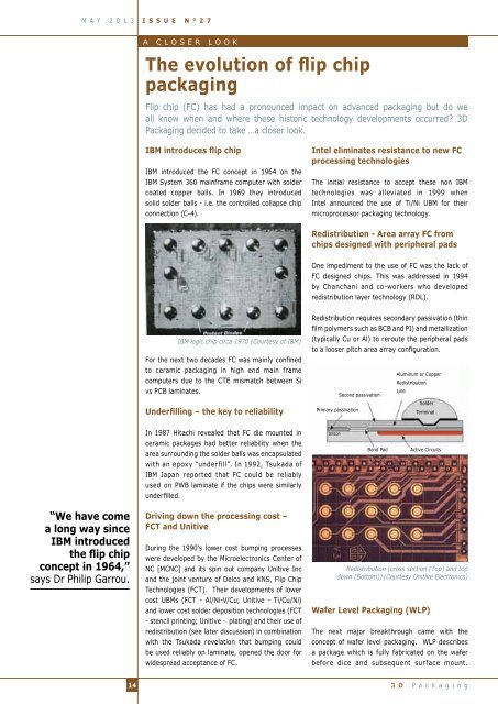
IBM logic chip circa 1970 (Courtesy of IBM)<br />
For the next two decades FC was mainly confined<br />
to ceramic packaging in high end main frame<br />
computers due to the CTE mismatch between Si<br />
vs PCB laminates.<br />
Underfilling – the key to reliability<br />
Redistribution requires secondary passivation (thin<br />
film polymers such as BCB and PI) and metallization<br />
(typically Cu or Al) to reroute the peripheral pads<br />
to a looser pitch area array configuration.<br />
Aluminum or Copper<br />
Redistribution<br />
Line<br />
Second passivation<br />
Solder<br />
Primary passivation<br />
Terminal<br />
In 1987 Hitachi revealed that FC die mounted in<br />
ceramic packages had better reliability when the<br />
area surrounding the solder balls was encapsulated<br />
with an epoxy “underfill”. In 1992, Tsukada of<br />
IBM Japan reported that FC could be reliably<br />
used on PWB laminate if the chips were similarly<br />
underfilled.<br />
Silicon<br />
Bond Pad<br />
Active Circuits<br />
“We have come<br />
a long way since<br />
IBM introduced<br />
the flip chip<br />
concept in 1964,”<br />
says Dr Philip Garrou.<br />
Driving down the processing cost –<br />
FCT and Unitive<br />
During the 1990’s lower cost bumping processes<br />
were developed by the Microelectronics Center of<br />
NC [MCNC] and its spin out company Unitive Inc<br />
and the joint venture of Delco and KNS, Flip Chip<br />
Technologies (FCT). Their developments of lower<br />
cost UBMs (FCT - Al/Ni-V/Cu; Unitive - Ti/Cu/Ni)<br />
and lower cost solder deposition technologies (FCT<br />
- stencil printing; Unitive - plating) and their use of<br />
redistribution (see later discussion) in combination<br />
with the Tsukada revelation that bumping could<br />
be used reliably on laminate, opened the door for<br />
widespread acceptance of FC.<br />
Redistribution (cross section (Top) and top<br />
down (Bottom)) (Courtesy Unitive Electronics)<br />
Wafer Level Packaging (WLP)<br />
The next major breakthrough came with the<br />
concept of wafer level packaging. WLP describes<br />
a package which is fully fabricated on the wafer<br />
before dice and subsequent surface mount.<br />
14<br />
3 D P a c k a g i n g


