

May 2013 - I-Micronews
May 2013 - I-Micronews
May 2013 - I-Micronews

Create successful ePaper yourself
Turn your PDF publications into a flip-book with our unique Google optimized e-Paper software.
I S S U E N ° 2 7 M A Y 2 0 1 3<br />
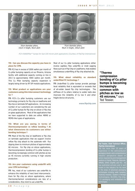
35um diameter pillars,<br />
23um in height, 50um pitch<br />
75um diameter pillars,<br />
40um in height, 100um pitch<br />
FCI’s NANOPillar TM bumps for Sub-100 micron pitch applications (Courtesy of FlipChip International)<br />
YD: Can you discuss the capacity you have in<br />
place for CPB.<br />
TT: FCI has in excess of 2000 wafers per month of<br />
Cu pillar bumping capacity at our Phoenix, Arizona<br />
facility with additional capacity coming on line in<br />
<strong>2013</strong> to approximately 4000 wafers per month.<br />
This Cu Pillar bumping capacity expansion is<br />
largely being driven by RF SiP module applications.<br />
YD: What product or applications are your<br />
customers using this interconnect technology<br />
for ?<br />
TT: FCI’s Cu pillar bumping customers use our<br />
technology primarily for flip chip on leadframe and<br />
flip chip on laminate SiP applications. An increasing<br />
number of our customers are considering the use<br />
of Cu pillar bumps for flip chip on silicon or flip chip<br />
on glass applications. Most of the applications that<br />
we have supported to date are either MEMS or<br />
MEMS-like types of applications.<br />
Most of our Cu pillar bumping applications either<br />
involve capillary flow underfills or mold capping<br />
flows such as in Flip Chip on Leadframe, that enables<br />
simultaneous underfilling of flip chip attached die.<br />
YD: What about reliability vs standard<br />
underfilled FC technology ?<br />
TT: Underfilled Cu pillar bumps provide package<br />
level reliability that is equivalent or exceeds that<br />
of all-solder based flip chip technologies. The<br />
stiffness of Cu pillars relative to solder balls also<br />
improves the reliability of Cu low K and other<br />
fragile device structures.<br />
www.flipchip.com<br />
“Thermo<br />
compression<br />
bonding of Cu pillar<br />
bumps is becoming<br />
increasingly<br />
common with<br />
pitches as low as<br />
45 microns,” says<br />
Ted Tessier.<br />
YD: What are you seeing in terms of<br />
thermocompression vs reflow bonding ? At<br />
what dimensions do customers use either<br />
bonding technique ?<br />
TT: Most of the flip chip on leadframe or flip chip<br />
on laminate applications that we support involve<br />
reflow flip chip attach to the substrate with flux<br />
dipping down to minimum pitches of approximately<br />
60 microns. For flip chip on silicon applications,<br />
thermocompression bonding of Cu pillar bumps is<br />
becoming increasingly common with pitches as low<br />
as 45 microns currently running in high volume<br />
production.<br />
YD: Are your customers using underfill with<br />
your CPB technology ?<br />
TT: Yes, most of our customers use underfills to<br />
enhance the reliability of next level interconnects.<br />
Even for flip chip on silicon applications, where<br />
thermomechanical considerations are less of a<br />
consideration, they tend to use underfills.<br />
3 D P a c k a g i n g<br />
Ted Tessier, Chief Technical Officer,<br />
FlipChip International<br />
Ted has more than 25 years of<br />
experience in the semiconductor<br />
packaging industry and a comprehensive<br />
industry perspective based on<br />
senior engineering and management<br />
positions at Nortel, Motorola, Biotronik,<br />
AMKOR, STATS ChipPAC and FCI. He<br />
has published actively and is well<br />
known in the industry for his work<br />
in the areas of advanced packaging<br />
technologies including wafer bumping,<br />
multichip modules / System in Package<br />
technologies, WLCSPs, flip chip,<br />
3 D packaging and embedded die<br />
technologies.<br />
11


