

May 2013 - I-Micronews
May 2013 - I-Micronews
May 2013 - I-Micronews

You also want an ePaper? Increase the reach of your titles
YUMPU automatically turns print PDFs into web optimized ePapers that Google loves.
I S S U E N ° 2 7 M A Y 2 0 1 3<br />
28nm, mass reflow will likely not be possible<br />
for reliability reasons, so we will have to move<br />
to copper pillar and thermal compression<br />
bonding directly. Then 3DIC/2.5D interposers<br />
will use copper pillar micro-bumping. Other<br />
more-than-Moore applications will also move<br />
to copper pillar for a variety of their own<br />
reasons, from image sensors needing higher<br />
density to power devices needing better<br />
thermal performance.<br />
Though the essential advantage of copper<br />
pillars is the tighter pitch possible with the<br />
straight-sided, high-aspect- ratio pillars and<br />
their smaller micro-bump cousins compared<br />
to the rounded form of solder bumps, the<br />
reduction of noise from the larger spacing<br />
between the pillars, and the better electrical<br />
conductivity compared to solder also improve<br />
performance. The downside, of course, is<br />
the higher cost and the immaturity of some<br />
of the processes, particularly probe and test.<br />
Progress will also be needed on finer precision<br />
in placement and bonding, and faster bonding<br />
with greater pressure. But we see few viable<br />
alternatives to copper pillar bumping going<br />
forward, especially for big ICs, and those with<br />
high numbers (~>800) of I/Os.<br />
Everybody adds capacity, looks at<br />
thermal compression bonding<br />
This growing demand is spurring investment<br />
across the value chain. Intel has long had<br />
the biggest copper bumping capacity, but<br />
foundries and OSATs are also both now<br />
investing aggressively, with recent investment<br />
by Samsung and TSMC on the foundry side,<br />
and Amkor and ASE on the OSAT side, driven<br />
primarily by 28nm CMOS. Most aggressive<br />
of all is PTI in Taiwan, who is investing some<br />
$300M over 2012-2014 to build and equip the<br />
world’s first fully dedicated fab for advanced<br />
bumping, to support its major customer<br />
Micron, but also to serving fabless customers<br />
like Qualcomm and non IC applications like<br />
MEMS from Toshiba. We see a 31% CAGR<br />
in additional copper pillar capacity brought<br />
online from 2010 to 2014, to bring it to 9<br />
million (12” eq) wafers a year. The industry’s<br />
copper bumping facilities have recently been<br />
running at ~88% capacity. This expanding<br />
cast of suppliers will expand availability of<br />
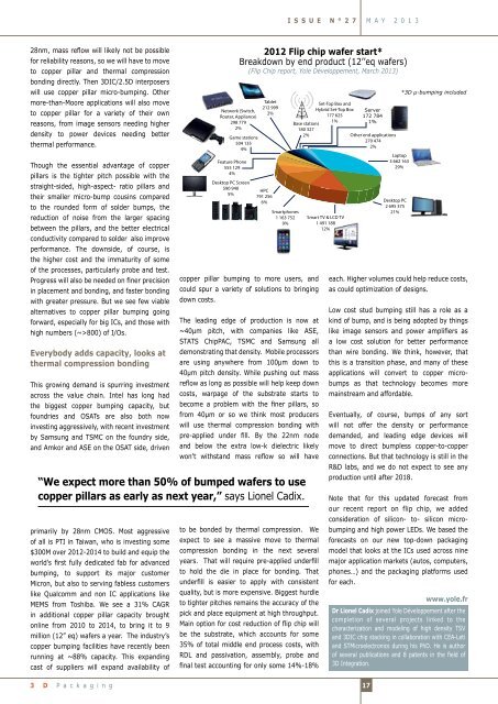
Network (Switch,<br />
Router, Appliance)<br />
298 779<br />
2%<br />
Game stations<br />
504 135<br />
4%<br />
Feature Phone<br />
555 129<br />
4%<br />
Desktop PC Screen<br />
590 940<br />
5%<br />
Tablet<br />
212 999<br />
2%<br />
HPC<br />
791 256<br />
6%<br />
Smartphones<br />
1 163 752<br />
9%<br />
copper pillar bumping to more users, and<br />
could spur a variety of solutions to bringing<br />
down costs.<br />
The leading edge of production is now at<br />
~40µm pitch, with companies like ASE,<br />
STATS ChipPAC, TSMC and Samsung all<br />
demonstrating that density. Mobile processors<br />
are using anywhere from 100µm down to<br />
40µm pitch density. While pushing out mass<br />
reflow as long as possible will help keep down<br />
costs, warpage of the substrate starts to<br />
become a problem with the finer pillars, so<br />
from 40µm or so we think most producers<br />
will use thermal compression bonding with<br />
pre-applied under fill. By the 22nm node<br />
and below the extra low-k dielectric likely<br />
won’t withstand mass reflow so will have<br />
“We expect more than 50% of bumped wafers to use<br />
copper pillars as early as next year,” says Lionel Cadix.<br />
2012 Flip chip wafer start*<br />
Breakdown by end product (12’’eq wafers)<br />
(Flip Chip report, Yole Développement, March <strong>2013</strong>)<br />
Base stations<br />
180 327<br />
2%<br />
to be bonded by thermal compression. We<br />
expect to see a massive move to thermal<br />
compression bonding in the next several<br />
years. That will require pre-applied underfill<br />
to hold the die in place for bonding. That<br />
underfill is easier to apply with consistent<br />
quality, but is more expensive. Biggest hurdle<br />
to tighter pitches remains the accuracy of the<br />
pick and place equipment at high throughput.<br />
Main option for cost reduction of flip chip will<br />
be the substrate, which accounts for some<br />
35% of total middle end process costs, with<br />
RDL and passivation, assembly, probe and<br />
final test accounting for only some 14%-18%<br />
Set-Top Box and<br />
Hybrid Set-Top Box<br />
177 625<br />
1%<br />
Smart TV & LCD TV<br />
1 491 188<br />
12%<br />
Server<br />
172 784<br />
1%<br />
Other end applications<br />
270 474<br />
2%<br />
Laptop<br />
3 662 163<br />
29%<br />
Desktop PC<br />
2 695 375<br />
21%<br />
*3D μ-bumping included<br />
each. Higher volumes could help reduce costs,<br />
as could optimization of designs.<br />
Low cost stud bumping still has a role as a<br />
kind of bump, and is being adopted by things<br />
like image sensors and power amplifiers as<br />
a low cost solution for better performance<br />
than wire bonding. We think, however, that<br />
this is a transition phase, and many of these<br />
applications will convert to copper microbumps<br />
as that technology becomes more<br />
mainstream and affordable.<br />
Eventually, of course, bumps of any sort<br />
will not offer the density or performance<br />
demanded, and leading edge devices will<br />
move to direct bumpless copper-to-copper<br />
connections. But that technology is still in the<br />
R&D labs, and we do not expect to see any<br />
production until after 2018.<br />
Note that for this updated forecast from<br />
our recent report on flip chip, we added<br />
consideration of silicon- to- silicon microbumping<br />
and high power LEDs. We based the<br />
forecasts on our new top-down packaging<br />
model that looks at the ICs used across nine<br />
major application markets (autos, computers,<br />
phones…) and the packaging platforms used<br />
for each.<br />
www.yole.fr<br />
Dr Lionel Cadix joined Yole Développement after the<br />
completion of several projects linked to the<br />
characterization and modeling of high density TSV<br />
and 3DIC chip stacking in collaboration with CEA-Leti<br />
and STMicroelectronics during his PhD. He is author<br />
of several publications and 8 patents in the field of<br />
3D Integration.<br />
3 D P a c k a g i n g<br />
17


