

May 2013 - I-Micronews
May 2013 - I-Micronews
May 2013 - I-Micronews

You also want an ePaper? Increase the reach of your titles
YUMPU automatically turns print PDFs into web optimized ePapers that Google loves.
M A Y 2 0 1 3 I S S U E N ° 2 7<br />
YOLE ASKS<br />
Keeping up with the industry<br />
heavyweights<br />
IBM may have invented flip chip and Intel may have brought it to the worlds<br />
microprocessors, but FCT, through its low cost processing technologies brought<br />
it to hand held products in the early 2000’s.<br />
Ted Tessier, Chief<br />
Technical Officer,<br />
FlipChip International<br />
FlipChip Int (FCI) began in 1996 as FlipChip<br />
Technologies (FCT), a joint venture between<br />
Delco electronics and Kulicke and Soffa<br />
(K&S). By modifying the Delco flip chip (FC)<br />
process, FCT was able to develop and license what<br />
quickly became the standard for flip chip bumping<br />
across the world. All of the major assembly<br />
houses including Amkor, ASE, STATS ChipPAC and<br />
Siliconware ran the FCT process.<br />
In 1998 FCT developed and patented the worlds<br />
first wafer level chip sized package (WLCSP), the<br />
Ultra CSP TM . In the early 2000’s estimates were<br />
that > 80% of cell phones contained FC or WLP<br />
parts derived from FCT processes.<br />
In 2004 RoseStreet Labs, a private R&D company<br />
based in Phoenix acquired FCT and renamed it<br />
FlipChip Int. Through the years FCI has managed to<br />
stay abreast of leading edge technologies and keep<br />
up with the industry “heavyweights”. i<strong>Micronews</strong><br />
recently had the opportunity to have a one-on-one<br />
with current CTO Ted Tessier to see where they<br />
stood on copper pillar bumping (CPB).<br />
Yole Développement: Is your organization<br />
manufacturing CPB technology? If yes can<br />
you share how long you have been doing this<br />
and describe the technology for us?<br />
Ted Tessier: FCI’s Cu pillar bumping process was<br />
qualified in 2007 and in volume production since<br />
2011. We offer a Standard Cu Pillar Bump for<br />
applications with bump pitches of 150 microns or<br />
less and our Nano-Pillar TM technology intended for<br />
sub-100 micron pitch applications.<br />
Our proprietary and patent pending technology is<br />
based on a solder paste printed solder cap. This<br />
approach enables a very broad range of solder<br />
alloys to be used vs traditional electroplated<br />
solder caps used by our competitors. This allows<br />
the Cu Pillar bump to be readily tailored to the<br />
reliability requirements of particular applications (i.e.<br />
automotive, hand-held consumer products etc…). A<br />
broad range of solder options have been qualified<br />
including High-Pb, Sn/Pb eutectic, Sn/Ag eutectic,<br />
pure Sn as well as High and Low Ag solder caps.<br />
For SiP packaging, a single solder alloy solution<br />
such as SAC305 or SAC405 is enabled.<br />
Solder capped pillar bump provides substantially<br />
improved bump height uniformity as a result of<br />
the inherent ability of the paste printed cap to<br />
compensate for Cu pillar plating variation. This is<br />
particularly important in device applications that<br />
require a range of different pillar bump sizes to<br />
balance the localized on-chip interconnection<br />
density / finer pitch requirements with improved<br />
thermal performance by well-placed large racetrack<br />
or breadloaf shaped bumps.<br />
YD: Has CPB become mainstream technology ?<br />
TT: Cu pillar bump technology has been a<br />
mainstream technology in high performance<br />
microprocessors for many years. Over the past<br />
half decade or so, the adoption of Cu pillar bumping<br />
for mid-range device applications has become<br />
common. More recently, Cu pillar is starting to<br />
be adopted selectively within the RF space, most<br />
commonly for applications that require higher<br />
levels of electrical performance.<br />
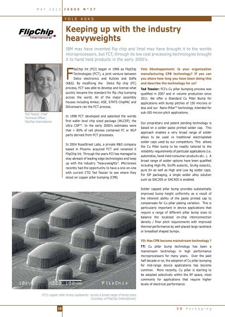
FCI’s copper pillar bump coplanarity: across a broad range of bump sizes<br />
(Courtesy of FlipChip International)<br />
10<br />
3 D P a c k a g i n g


