

May 2013 - I-Micronews
May 2013 - I-Micronews
May 2013 - I-Micronews

Create successful ePaper yourself
Turn your PDF publications into a flip-book with our unique Google optimized e-Paper software.
M A Y 2 0 1 3 I S S U E N ° 2 7<br />
A CLOSER LOOK<br />
Will CPB be the next evolution of FC?<br />
Microbumping, a.k.a. Copper Pillar Bumping appears to be the next evolution of flip<br />
chip technology. Is this technology really mainstream ? What is its status today?<br />
3D Packaging decided we should take – A Closer Look<br />
D<br />
The concept of interconnecting a chip in a<br />
face down or “flip chip” (FC) orientation<br />
can be traced back to IBM’s introduction of<br />
their system 360 mainframe computer in 1964.<br />
In the 1970s Delco Electronics developed FC<br />
for automotive applications but in general, for<br />
the next two decades FC was mainly confined<br />
to high end main frame computers (IBM, NEC,<br />
Fujitsu, Hitachi) because of reliability limitations<br />
due to the mismatch between the coefficient of<br />
thermal expansion (CTE) of Silicon (Si), solder and<br />
substrate (ceramic, PCB).<br />
As transistors continued to shrink, the increased<br />
number of circuits per chip required more I/O which<br />
eventually caught up with traditional IC designs<br />
where pads were placed on the periphery to allow<br />
interconnection by wire bonding to a lead frame.<br />
It was obvious that higher I/O counts could only be<br />
obtained by moving to area array packaging and<br />
that required flip chip.<br />
The development of lower cost sputtered UBMs<br />
and lower cost stencil printed solder deposition<br />
technology at FCT (1996-1998) in combination with<br />
the IBM Japan revelation (1992) that underfilled<br />
bumping could be used reliably on laminate,<br />
opened the door for widespread adoption of this<br />
high performance interconnection technology in<br />
the late 1990’s.<br />
The FCT “flex-on-cap” and “Ultra CSP” technologies<br />
were licensed by all the key assembly houses as<br />
they initiated production in 1999 - 2001 including:<br />
P<br />
ASE, Amkor, STATS ChipPAC, SPIL and others.<br />
Most of the world’s production is still done today<br />
using these or similar technologies.<br />
But today, in order to deliver even higher<br />
interconnect densities, i.e. “micro-bumping”, the<br />
industry is having to adopt Copper pillar bumping<br />
(CPB). Is this technology really mainstream? What<br />
is its status today? 3D Packaging decided we<br />
should take “A Closer Look”.<br />
We have sought the input experts from several<br />
different segments of the industry infrastructure<br />
Manufacturing capacity<br />
Bob Lanzone notes that “Amkor was the first OSAT<br />
to develop and create HVM for this technology and<br />
put large scale capacity in place to serve numerous<br />
customers in 2010…We have shipped over 200<br />
million units thus far”. In terms of capacity,<br />
Lanzone states that Amkor has “…30K 300 mm<br />
wafers per month CPB capacity” and a packaging<br />
capacity of 15 MM units per month.<br />
Mike Ma, VP of Corporate R&D for Siliconware<br />
Precision Industries (SPIL), indicates that SPIL<br />
has been in CPB production for “…over 2 years”.<br />
Ma noted that their current capacity is 20K units/<br />
month with plans to expand to 60K units/month in<br />
4Q <strong>2013</strong>. Ma sees CPB already being “mainstream…<br />
especially in communication application devices.”<br />
Remi Yu, Deputy Director of marketing at foundry<br />
UMC, does not have wafer bumping in house<br />
but rather “…collaborates with qualified OSATs<br />
to provide bump solutions to our customers…”.<br />
Yu notes that “…some customers [are] already<br />
defining Cu pillar bump as the process of record at<br />
28 nm node”.<br />
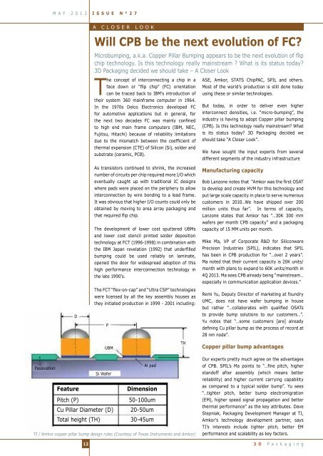
UBM<br />
TH<br />
Copper pillar bump advantages<br />
Al pad<br />
Passivation<br />
Si Wafer<br />
Feature<br />
Dimension<br />
Pitch (P)<br />
50-100um<br />
Cu Pillar Diameter (D) 20-50um<br />
Total height (TH)<br />
30-45um<br />
TI / Amkor copper pillar bump design rules (Courtesy of Texas Instruments and Amkor)<br />
12<br />
Our experts pretty much agree on the advantages<br />
of CPB. SPIL’s Ma points to “…fine pitch, higher<br />
standoff after assembly (which means better<br />
reliability) and higher current carrying capability<br />
as compared to a typical solder bump”. Yu sees<br />
“…tighter pitch, better bump electromigration<br />
(EM), higher speed signal propagation and better<br />
thermal performance” as the key attributes. Dave<br />
Stepniak, Packaging Development Manager at TI,<br />
Amkor’s technology development partner, says<br />
TI’s interests include tighter pitch, better EM<br />
performance and scalability as key factors.<br />
3 D P a c k a g i n g


