

May 2013 - I-Micronews
May 2013 - I-Micronews
May 2013 - I-Micronews

Create successful ePaper yourself
Turn your PDF publications into a flip-book with our unique Google optimized e-Paper software.
I S S U E N ° 2 7 M A Y 2 0 1 3<br />
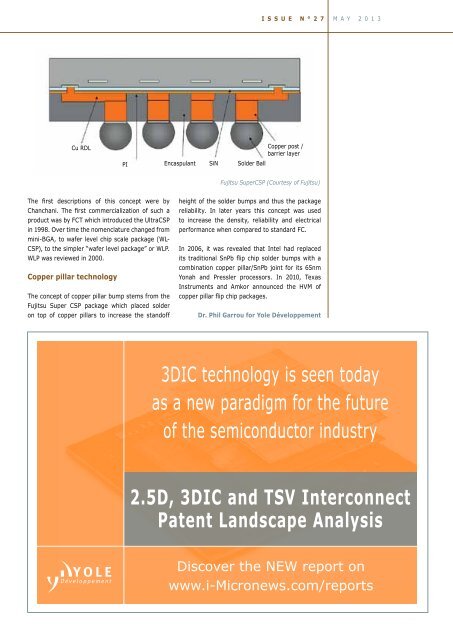
Cu RDL<br />
Copper post /<br />
barrier layer<br />
PI Encaspulant SiN Solder Ball<br />
Fujitsu SuperCSP (Courtesy of Fujitsu)<br />
The first descriptions of this concept were by<br />
Chanchani. The first commercialization of such a<br />
product was by FCT which introduced the UltraCSP<br />
in 1998. Over time the nomenclature changed from<br />
mini-BGA, to wafer level chip scale package (WL-<br />
CSP), to the simpler “wafer level package” or WLP.<br />
WLP was reviewed in 2000.<br />
Copper pillar technology<br />
The concept of copper pillar bump stems from the<br />
Fujitsu Super CSP package which placed solder<br />
on top of copper pillars to increase the standoff<br />
height of the solder bumps and thus the package<br />
reliability. In later years this concept was used<br />
to increase the density, reliability and electrical<br />
performance when compared to standard FC.<br />
In 2006, it was revealed that Intel had replaced<br />
its traditional SnPb flip chip solder bumps with a<br />
combination copper pillar/SnPb joint for its 65nm<br />
Yonah and Pressler processors. In 2010, Texas<br />
Instruments and Amkor announced the HVM of<br />
copper pillar flip chip packages.<br />
Dr. Phil Garrou for Yole Développement<br />
3DIC technology is seen today<br />
as a new paradigm for the future<br />
of the semiconductor industry<br />
2.5D, 3DIC and TSV Interconnect<br />
Patent Landscape Analysis<br />
Discover the NEW report on<br />
www.i-<strong>Micronews</strong>.com/reports


