

May 2013 - I-Micronews
May 2013 - I-Micronews
May 2013 - I-Micronews

Create successful ePaper yourself
Turn your PDF publications into a flip-book with our unique Google optimized e-Paper software.
M A Y 2 0 1 3 I S S U E N ° 2 7<br />
ANALYST CORNER<br />
Mainstream flip chip bumping starts<br />
to move to copper pillars<br />
Copper pillars and micro bumps will soon re-shape the flip chip market and supply<br />
chain, as mobile processors, memory, and non-mainstream CMOS devices start<br />
to require smaller geometries, higher I/O counts, higher bandwidth, and better<br />
thermal management. That will propel 9% growth for the flip chip packaging<br />
market through 2018, with most of that growth driven by the emerging copper<br />
technologies.<br />
Lionel Cadix,<br />
Market & Technology<br />
Analyst, Advanced<br />
Packaging,<br />
Yole Développement<br />
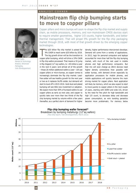
The $20 billion flip chip market is poised for<br />
9% CAGR to reach some $35 billion by 2018.<br />
The big growth driver will be the transition to<br />
copper pillar bumping, which will drive a 19% CAGR<br />
in flip chip wafers processed. That means a 3X jump<br />
in flip chipped (12” eq) wafers, to ~40 million a year<br />
in the next 6 years—and almost all of the growth<br />
--those 26 million additional wafers a year-- will use<br />
copper pillars or micro-bumps, as copper comes to<br />
increasingly dominate the flip chip market. Leadfree<br />
solder will see healthy growth for the next year<br />
or two as it replaces Sn/Pb solder, but demand will<br />
start to level off in 2015-2016. Gold stud and plated<br />
bumping will see little new investment or adoption.<br />
We expect more than 50% of bumped wafers to use<br />
copper pillars as early as next year, and copper to<br />
quickly take over more than two thirds of the flip<br />
chip bumping market by volume within a few years<br />
thereafter, as a perfect storm of demand for higher<br />
density, higher performance interconnect develops.<br />
Demand will come from a variety of applications.<br />
In 2012, logic for personal computers and laptops<br />
accounted for more than half the flip chip bumping<br />
market, with much of the rest used in mobile<br />
phones and high performance computers. But<br />
that mix will soon change as 28nm devices need<br />
higher density connections than possible with<br />
solder bumps, with demand driven especially by<br />
application processors for mobile phones, and<br />
mobile applications will quickly become the main<br />
driving market for copper pillars. Next application<br />
will likely be memory, which we also expect to start<br />
to move quickly to copper pillars in the next couple<br />
of years, starting with DDR4 and wide I/O, driven<br />
by the need for fine pitch for high bandwidth and<br />
high I/O count, to decrease delay and decrease<br />
power consumption, as wire bonding parasitics<br />
become more problematic. For memory below<br />
Flip chip bumping wafer forecast*<br />
Breakdown by bumping metallurgy (12’’eq wafers)<br />
(Flip Chip report, Yole Développement, March <strong>2013</strong>)<br />
Millions<br />
45<br />
40<br />
*3D µ-bumping included<br />
35<br />
30<br />
Wafer count (12''eq)<br />
25<br />
20<br />
15<br />
Cu pillar<br />
Lead free solder<br />
Sn/Pb eutectic solder<br />
Gold stud + plated<br />
10<br />
5<br />
0<br />
2010 2011 2012 <strong>2013</strong> 2014 2015 2016 2017 2018<br />
16<br />
3 D P a c k a g i n g


