

May 2013 - I-Micronews
May 2013 - I-Micronews
May 2013 - I-Micronews

You also want an ePaper? Increase the reach of your titles
YUMPU automatically turns print PDFs into web optimized ePapers that Google loves.
M A Y 2 0 1 3 I S S U E N ° 2 7<br />
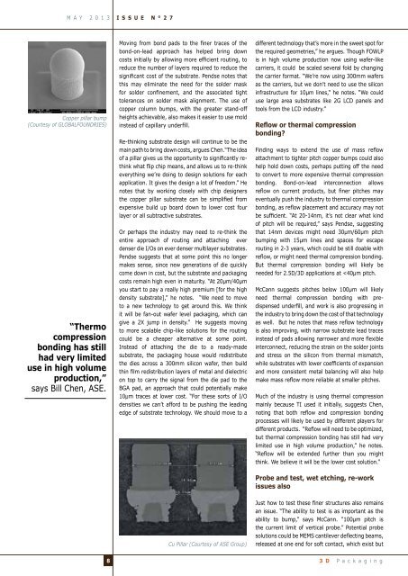
Copper pillar bump<br />
(Courtesy of GLOBALFOUNDRIES)<br />
“Thermo<br />
compression<br />
bonding has still<br />
had very limited<br />
use in high volume<br />
production,”<br />
says Bill Chen, ASE.<br />
Moving from bond pads to the finer traces of the<br />
bond-on-lead approach has helped bring down<br />
costs initially by allowing more efficient routing, to<br />
reduce the number of layers required to reduce the<br />
significant cost of the substrate. Pendse notes that<br />
this may eliminate the need for the solder mask<br />
for solder confinement, and the associated tight<br />
tolerances on solder mask alignment. The use of<br />
copper column bumps, with the greater stand-off<br />
heights achievable, also makes it easier to use mold<br />
instead of capillary underfill.<br />
Re-thinking substrate design will continue to be the<br />
main path to bring down costs, argues Chen.“The idea<br />
of a pillar gives us the opportunity to significantly rethink<br />
what flip chip means, and allows us to re-think<br />
everything we’re doing to design solutions for each<br />
application. It gives the design a lot of freedom.” He<br />
notes that by working closely with chip designers<br />
the copper pillar substrate can be simplified from<br />
expensive build up board down to lower cost four<br />
layer or all subtractive substrates.<br />
Or perhaps the industry may need to re-think the<br />
entire approach of routing and attaching ever<br />
denser die I/Os on ever denser multilayer substrates.<br />
Pendse suggests that at some point this no longer<br />
makes sense, since new generations of die quickly<br />
come down in cost, but the substrate and packaging<br />
costs remain high even in maturity. “At 20µm/40µm<br />
you start to pay a really high premium [for the high<br />
density substrate],” he notes. “We need to move<br />
to a new technology to get around this. We think<br />
it will be fan-out wafer level packaging, which can<br />
give a 2X jump in density.” He suggests moving<br />
to more scalable chip-like solutions for the routing<br />
could be a cheaper alternative at some point.<br />
Instead of attaching the die to a ready-made<br />
substrate, the packaging house would redistribute<br />
the dies across a 300mm silicon wafer, then build<br />
thin film redistribution layers of metal and dielectric<br />
on top to carry the signal from the die pad to the<br />
BGA pad, an approach that could potentially make<br />
10µm traces at lower cost. “For these sorts of I/O<br />
densities we can’t afford to be pushing the leading<br />
edge of substrate technology. We should move to a<br />
different technology that’s more in the sweet spot for<br />
the required geometries,” he argues. Though FOWLP<br />
is in high volume production now using wafer-like<br />
carriers, it could be scaled several fold by changing<br />
the carrier format. “We’re now using 300mm wafers<br />
as the carriers, but we don’t need to use the silicon<br />
infrastructure for 10µm lines,” he notes. “We could<br />
use large area substrates like 2G LCD panels and<br />
tools from the LCD industry.”<br />
Reflow or thermal compression<br />
bonding?<br />
Finding ways to extend the use of mass reflow<br />
attachment to tighter pitch copper bumps could also<br />
help hold down costs, perhaps putting off the need<br />
to convert to more expensive thermal compression<br />
bonding. Bond-on-lead interconnection allows<br />
reflow on current products, but finer pitches may<br />
eventually push the industry to thermal compression<br />
bonding, as reflow placement and accuracy may not<br />
be sufficient. “At 20-14nm, it’s not clear what kind<br />
of pitch will be required,” says Pendse, suggesting<br />
that 14nm devices might need 30µm/60µm pitch<br />
bumping with 15µm lines and spaces for escape<br />
routing in 2-3 years, which could be still doable with<br />
reflow, or might need thermal compression bonding.<br />
But thermal compression bonding will likely be<br />
needed for 2.5D/3D applications at


