

May 2013 - I-Micronews
May 2013 - I-Micronews
May 2013 - I-Micronews

Create successful ePaper yourself
Turn your PDF publications into a flip-book with our unique Google optimized e-Paper software.
I S S U E N ° 2 7<br />
M A Y 2 0 1 3<br />
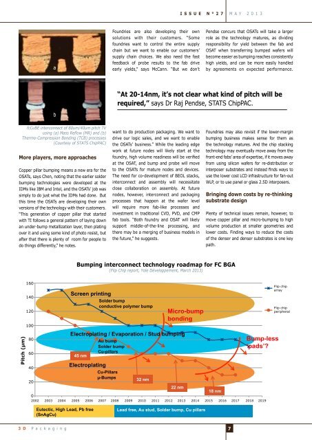
a<br />
Foundries are also developing their own<br />
solutions with their customers. “Some<br />
foundries want to control the entire supply<br />
chain but we want to enable our customers’<br />
supply chain choices. We also need the fast<br />
feedback of probe results to the fab drive<br />
early yields,” says McCann. “But we don’t<br />
Pendse concurs that OSATs will take a larger<br />
role as the technology matures, as dividing<br />
responsibility for yield between the fab and<br />
OSAT when transferring bumped wafers will<br />
become easier as bumping reaches consistently<br />
high yields, and can be more easily handled<br />
by agreements on expected performance.<br />
“At 20-14nm, it’s not clear what kind of pitch will be<br />
required,” says Dr Raj Pendse, STATS ChipPAC.<br />
b<br />
fcCuBE interconnect of 80um/40um pitch TV<br />
using (a) Mass Reflow (MR) and (b)<br />
Thermo-Compression Bonding (TCB) processes<br />
(Courtesy of STATS ChipPAC)<br />
More players, more approaches<br />
Copper pillar bumping means a new era for the<br />
OSATs, says Chen, noting that the earlier solder<br />
bumping technologies were developed at the<br />
IDMs like IBM and Intel, and the OSATs’ job was<br />
simply to do just what the IDMs had done. But<br />
this time the OSATs are developing their own<br />
versions of the technology with their customers.<br />
“This generation of copper pillar that started<br />
with TI follows a general pattern of laying down<br />
an under-bump metallization layer, then plating<br />
over it and using some kind of photo resist, but<br />
after that there is plenty of room for people to<br />
do things differently,” he notes.<br />
want to do production packaging. We want to<br />
drive our logic sales, and we want to enable<br />
the OSATs’ business.” While the leading edge<br />
work at future nodes will likely start at the<br />
foundry, high volume readiness will be verified<br />
at the OSAT, and bump and probe will move<br />
to the OSATs for mature nodes and devices.<br />
The need for co-development of BEOL stacks,<br />
interconnect and assembly will necessitate<br />
close collaboration on assembly. At future<br />
nodes, however, interconnect and packaging<br />
processes that happen at the wafer level<br />
will require more fab-like processes and<br />
investment in traditional CVD, PVD, and CMP<br />
fab tools. “Both foundry and OSAT will likely<br />
support middle-of-the-line processing, and<br />
there may be a merging of business models in<br />
the future,” he suggests.<br />
Foundries may also revisit if the lower-margin<br />
bumping business makes sense for them as<br />
the technology matures. And the chip stacking<br />
technology may eventually move away from the<br />
front-end fabs’ area of expertise, if it moves away<br />
from using silicon wafers for re-distribution or<br />
interposer substrates and instead finds ways to<br />
use the lower cost LCD infrastructure for fan-out<br />
WLP, or to use panel or glass 2.5D interposers.<br />
Bringing down costs by re-thinking<br />
substrate design<br />
Plenty of technical issues remain, however, to<br />
move copper pillar and micro-bumping to high<br />
volume production at smaller geometries and<br />
lower costs. Finding ways to reduce the costs<br />
of the denser and denser substrates is one key<br />
path.<br />
Bumping interconnect technology roadmap for FC BGA<br />
(Flip Chip report, Yole Développement, March <strong>2013</strong>)<br />
Pitch (µm)<br />
160<br />
140<br />
120<br />
100<br />
80<br />
60<br />
Screen printing<br />
45 nm<br />
Electroplating<br />
Solder bump<br />
conductive polymer bump<br />
Electroplating / Evaporation / Stud bumping<br />
Au bump<br />
Solder bump<br />
Cu-pillars<br />
Micro-bump<br />
bonding<br />
Bump-less<br />
‘pads’?<br />
40<br />
Cu-Pillars<br />
µ-Bumps<br />
20<br />
32 nm<br />
22 nm<br />
18 nm<br />
0<br />
2002 2003 2004 2005 2006 2007 2008 2009 2010 2011 2012 <strong>2013</strong> 2014 2015 2016 2017 2018 2019<br />
Flip chip<br />
array<br />
Flip chip<br />
peripheral<br />
Eutectic, High Lead, Pb free<br />
(SnAgCu)<br />
Lead free, Au stud, Solder bump, Cu pillars<br />
3 D P a c k a g i n g<br />
7


