Synchronous Latency Insensitive Design - ICS
Synchronous Latency Insensitive Design - ICS
Synchronous Latency Insensitive Design - ICS
Create successful ePaper yourself
Turn your PDF publications into a flip-book with our unique Google optimized e-Paper software.
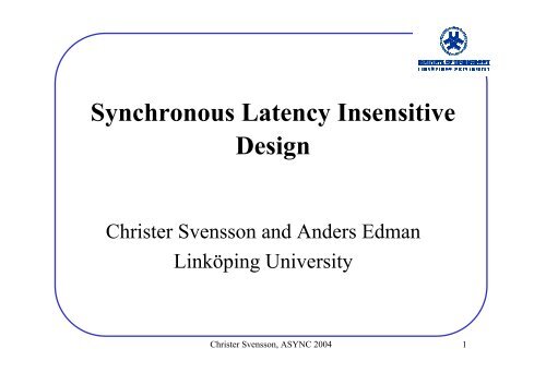
<strong>Synchronous</strong> <strong>Latency</strong> <strong>Insensitive</strong><br />
<strong>Design</strong><br />
Christer Svensson and Anders Edman<br />
Linköping University<br />
Christer Svensson, ASYNC 2004 1
Outline<br />
• Introduction<br />
• Overview of wire properties<br />
• Architectural view of future systems<br />
• <strong>Synchronous</strong> <strong>Latency</strong> <strong>Insensitive</strong> <strong>Design</strong><br />
• Multiple clocks<br />
• Conclusion<br />
Christer Svensson, ASYNC 2004 2
Introduction<br />
The wire delay problem was recognized very early (Anceau 1982)<br />
Wire delay ~ L 2 /s 2 , Gate delay ~s α , s=feature size, α=1..2<br />
In spite of the “alarm” 1982, we still manage multigigahertz synchronous<br />
designs, BUT today with considerable problems.<br />
ASIC style designs normally limited to 300-500MHz clock, with severe<br />
“timing closure” problems.<br />
Multigigahertz designs very demanding full custom design style.<br />
Christer Svensson, ASYNC 2004 3
Introduction<br />
<strong>Synchronous</strong> design paradigm VERY established – we need to keep.<br />
(Easy to keep track on exact timing of all events; predictable performance)<br />
Vast experience used to manage ever increasing complexity.<br />
Critical: Timing relations between clock and data<br />
Present solution:<br />
“Flat” clock distribution (skew-free clock)<br />
Does not solve problem with data delays<br />
clk<br />
Balanced clk net - no skew<br />
Wire delay still affects data<br />
Christer Svensson, ASYNC 2004 4
Overview of wire properties<br />
Ground planes<br />
Twisted<br />
pair<br />
Cables<br />
Coaxial<br />
cable<br />
Microstrip<br />
Coplanar waveguide<br />
Circuit boards and chips<br />
We will concentrate on microstrip<br />
in the following<br />
Christer Svensson, ASYNC 2004 5
Overview of wire properties<br />
Skin effect loss<br />
Higher frequencies - skineffekt<br />
Fields penetrate metal to skin-depth δ<br />
Resistance per unit length, r:<br />
r = r s<br />
ω<br />
Including current phase and low frequency resistance:<br />
Current flow, depth δ, (skin depth)<br />
r<br />
= rDC + rs<br />
1+<br />
( j) ω<br />
Frequency dependence (dispersion) gives rise to signal distortion<br />
Christer Svensson, ASYNC 2004 6
Overview of wire properties<br />
We discuss 2 wire properties in the following<br />
Delay (<strong>Latency</strong>)<br />
Capacity (Maximum data rate)<br />
Christer Svensson, ASYNC 2004 7
Overview of wire properties<br />
Delay or latency, RC-wire<br />
High loss case (RC-case), r DC L/Z 0 >2ln2. Elmore delay good approximation:<br />
t<br />
d<br />
⎛<br />
⎜ R<br />
⎝<br />
⎛ C<br />
⎜<br />
⎝ 2<br />
⎞⎞<br />
⎟<br />
⎠⎠<br />
w<br />
( C + C + C ) + R + C ⎟ln<br />
2<br />
=<br />
S S w L w<br />
L<br />
<strong>Latency</strong> can be improved<br />
by repeaters<br />
Delay or latency, LC-wire<br />
Low loss case (LC-case), r DC L/Z 0
Overview of wire properties<br />
Capacity or maximum data rate<br />
T<br />
S(T)<br />
Single pulse<br />
Eye diagram<br />
Eye opening<br />
Eye opening = 2S(T)-1, S(t) step response, T symbol time<br />
We need a minimum opening for safe data detection, say 64%<br />
For long wires we may afford a simple equalizer, allowing 0%<br />
Christer Svensson, ASYNC 2004 9
Overview of wire properties<br />
Capacity or maximum data rate<br />
RC-wire: Step response:<br />
S<br />
−<br />
2T<br />
R w<br />
( ) w C<br />
T = 1−<br />
e<br />
Eye opening of 64% yields S(T)=0.82 or T=0.85R w C w<br />
Max data rate<br />
LC-wire: Step response (skin effect):<br />
Max data rate,<br />
B<br />
1<br />
=<br />
T<br />
B = b<br />
=<br />
LC<br />
b<br />
RC<br />
A<br />
2<br />
L<br />
A<br />
2<br />
L<br />
S<br />
( T )<br />
= 1−<br />
erf<br />
⎛<br />
⎜<br />
⎝<br />
2Z<br />
ρµ<br />
0<br />
w<br />
0<br />
L<br />
T<br />
⎞<br />
⎟<br />
⎠<br />
Christer Svensson, ASYNC 2004 10
Overview of wire properties<br />
Note the difference between latency and data rate<br />
RC case<br />
t d<br />
T s >t d<br />
(wave pipelining, Xu 2003)<br />
LC case<br />
t d<br />
T s
Overview of wire properties<br />
Estimated data-rates<br />
Top metal<br />
chip wire<br />
10Gb/s<br />
@ 15mm<br />
Typical<br />
Board<br />
wire<br />
10Gb/s<br />
@ 0.5m<br />
Low level<br />
metal wire<br />
10Gb/s<br />
@ 1mm<br />
Low delay<br />
region<br />
Christer Svensson, ASYNC 2004 12
Overview of wire properties<br />
Low level on-chip wires<br />
Wire delay limits diameter of synchronous block<br />
System partition – “Global Asynchronous Local <strong>Synchronous</strong>”<br />
Upper on-chip wires<br />
Low delay, high data-rate global communication<br />
Inter-block communication<br />
Circuit board wires<br />
Can be used at least to 10Gb/s per wire<br />
Facilitates very high on-board bandwidths<br />
Christer Svensson, ASYNC 2004 13
Overview of wire properties<br />
On-chip local<br />
Future processes, feature size f=0.1 - 0.035 µm<br />
wire cross section ~3f 2 , for 0.1µm: 3·10 -14 m 2<br />
10Gb/s up to 1.25mm length<br />
1mm wire will have a delay of 26ps (26% of 10GHz clock cycle)<br />
We may use 10GHz clock frequency in fully synchronous block<br />
of diameter 1mm. Such a block can contain 250,000 gates.<br />
(Compare to Sylvester and Keutzler 50-100 kgates)<br />
Note that diameter scales as f 2 ; number of gates as f -2<br />
so 250 kgates is kept until 0.035µm (or further) at 10GHz.<br />
Christer Svensson, ASYNC 2004 14
Overview of wire properties<br />
On-chip global<br />
Traditional alternative<br />
Automatic insertion of repeaters along long wires<br />
With wave pipelining allows >10Gb/s per wire<br />
Delays may exceed one clock cycle<br />
Utilizing upper thick metal layer<br />
Data rate >10Gb/s<br />
Delays close to velocity-of-light, still order of one clock cycle<br />
Christer Svensson, ASYNC 2004 15
Overview of wire properties<br />
Upper wire/driver example<br />
Inverter in 0.18µm CMOS<br />
W n =88µm, w p =194µm, R S =20Ω<br />
Actual step response<br />
Step response<br />
without overdrive<br />
Step response, terminated<br />
3.5µm<br />
2µm<br />
Wire length 2cm<br />
4µm 12µm<br />
2µm x 4µm copper wire, low loss<br />
12µm spacing, X-talk
Overview of wire properties<br />
Upper wire/driver example<br />
Estimated performance (length 2cm)<br />
• Simulated velocity: 10 8 m/s (c 0 /3)<br />
• Simulated maximum data-rate 10Gb/s<br />
• Each link is 16 bit wide, 2 links carry 320Gb/s (bidirectionally)<br />
• Each 2 links need 544µm width<br />
Christer Svensson, ASYNC 2004 17
Architectural view of future systems<br />
Chip<br />
On-chip global links<br />
Chip<br />
<strong>Synchronous</strong><br />
blocks<br />
High speed<br />
board links<br />
Clock<br />
Christer Svensson, ASYNC 2004 18
Architectural view of future systems<br />
Chip<br />
On-chip global links<br />
Chip<br />
Challenges<br />
<strong>Synchronous</strong><br />
blocks<br />
Allow scaling of clock rates and bandwidths<br />
Mitigate synchronization and clock skew problems<br />
Keep an unchanged synchronous High speed design paradigm<br />
board links<br />
Clock<br />
Christer Svensson, ASYNC 2004 19
Architectural view of future systems<br />
Wire delays are inevitable: we must accept latency.<br />
The latency/delay problem should be managed at two levels<br />
• System level (predictability)<br />
• Implementation level (error-free)<br />
Christer Svensson, ASYNC 2004 20
Architectural view of future systems<br />
System level.<br />
Partition the system into blocks of limited size.<br />
(Preferably natural partition, processors, memories, IP-blocks etc.)<br />
We may define a system where only order of events is important.<br />
(“Classical” asynchronous, Patient systems (Carloni et al 1999))<br />
We may then accept any latency between blocks.<br />
We may define a system with fixed latency between blocks.<br />
(If fixed latency is n clock cycles, the system is synchronous)<br />
We may then accept any latency < nT c between blocks.<br />
Christer Svensson, ASYNC 2004 21
Architectural view of future systems<br />
Implementation level (We must avoid synchronization errors)<br />
Use synchronizers with long decision time<br />
(extra latency, nonzero error probability)<br />
Use stoppable clocks to synchronize communication<br />
(Classical GALS, Chapiro 1984)<br />
Adapt clock phase to data (mesochronous clocks)<br />
(Mu 2001)<br />
Use FIFO’s to isolate clock regions<br />
(FIFO’s initialized with synchronizers, Chakraborty 2001)<br />
(FIFO’s initialized via system reset, Edman 2004)<br />
Christer Svensson, ASYNC 2004 22
Architectural view of future systems<br />
Implementation level, Examples<br />
Data in<br />
Choise of clock phase<br />
(Mu 2001)<br />
Metastab.<br />
detector<br />
Data out<br />
Rx clk<br />
FIFO solution<br />
(Chakraborty 2001,<br />
Edman 2004)<br />
Data in<br />
Write<br />
pointer<br />
Read<br />
pointer<br />
Data out<br />
Tx clk<br />
Rx clk<br />
“Circular” FIFO<br />
Christer Svensson, ASYNC 2004 23
<strong>Synchronous</strong> <strong>Latency</strong> <strong>Insensitive</strong> <strong>Design</strong><br />
Problem formulation<br />
Find a method to mitigate wire-induced latencies within a<br />
synchronous paradigm<br />
Christer Svensson, ASYNC 2004 24
<strong>Synchronous</strong> <strong>Latency</strong> <strong>Insensitive</strong> <strong>Design</strong><br />
Concept<br />
Clock true model<br />
Fixed delays (n clk cycles)<br />
Communication links<br />
clk<br />
<strong>Synchronous</strong><br />
blocks<br />
Synthesis<br />
During synthesis we<br />
replace Fixed delays with<br />
synchronizing ports<br />
(elastic FIFOs) that absorb<br />
all link latencies and<br />
clock skews.<br />
Final design agree exactly<br />
with Clock true model<br />
independently of<br />
link delays and clock skews.<br />
Christer Svensson, ASYNC 2004 25
<strong>Synchronous</strong> <strong>Latency</strong> <strong>Insensitive</strong> <strong>Design</strong><br />
System<br />
partition<br />
<strong>Design</strong> flow<br />
“Natural” partition (processors, memories,<br />
IP-blocks…) into isochronous regions<br />
Clock-true<br />
model &<br />
verification<br />
NEW: Insertion of dummy delays between<br />
isochronic regions. Clock-true verification.<br />
Synthesis &<br />
Back-end<br />
Replace dummy delays with elastic FIFO’s<br />
Timing<br />
verification<br />
Considerably easier, feedback can be avoided<br />
Christer Svensson, ASYNC 2004 26
<strong>Synchronous</strong> <strong>Latency</strong> <strong>Insensitive</strong> <strong>Design</strong><br />
Implementation<br />
data<br />
reg<br />
reg<br />
data<br />
data<br />
strobe<br />
clk<br />
Example with three blocks<br />
and two links<br />
select<br />
Input<br />
counter<br />
strobe<br />
Output<br />
counter<br />
Local<br />
clock<br />
Synchronizing port<br />
Fixed nominal delay preset in counters<br />
Christer Svensson, ASYNC 2004 27
<strong>Synchronous</strong> <strong>Latency</strong> <strong>Insensitive</strong> <strong>Design</strong><br />
Implementation<br />
System reset used as initialization mechanism (example n=2)<br />
clk<br />
Tx1<br />
rst<br />
written into<br />
FIFO(2) by strobe<br />
reset<br />
clk at root<br />
data at Tx1<br />
data at Rx<br />
Tx2<br />
read from FIFO(2) by<br />
Rx clk after 2 counts<br />
FIFO(2)<br />
clk at Rx<br />
Rx<br />
data in Rx<br />
Note that data relation to clk period number predictable<br />
Christer Svensson, ASYNC 2004 28
<strong>Synchronous</strong> <strong>Latency</strong> <strong>Insensitive</strong> <strong>Design</strong><br />
Simulation<br />
clk<br />
Tx1<br />
Clk<br />
Tx1 out<br />
Rx1 in<br />
Tx2 out<br />
Rx2 in<br />
Rx1 out<br />
Rx2 out<br />
Rx1 in count<br />
Rx1 out count<br />
Rx2 in count<br />
Rx2 out count<br />
00 01 10 11 00 01 10 11 00 01<br />
10 11 00 01 10 11 00 01 10 11 00 01<br />
00 01 10 11 00 01 10 11 00 01 10<br />
10 11 00 01 10 11 00 01 10 11 00 01<br />
Rx<br />
Tx2<br />
0 20 ns 40 ns 60 ns<br />
Clk<br />
Tx1 out<br />
Rx1 in<br />
Tx2 out<br />
Rx2 in<br />
Rx1 out<br />
Rx2 out<br />
Rx1 in count 00 01 10 11 00 01 10 11 00 01<br />
Rx1 out count 10 11 00 01 10 11 00 01 10 11<br />
Rx2 in count 00 01 10 11 00 01 10 11 00 01 10<br />
11<br />
Rx2 out count 10 11 00 01 10 11 00 01 10<br />
0 20 ns 40 ns 60 ns<br />
Christer Svensson, ASYNC 2004 29
<strong>Synchronous</strong> <strong>Latency</strong> <strong>Insensitive</strong> <strong>Design</strong><br />
Implementation example, receiver in 0.18µm CMOS<br />
f c =2.75GHz<br />
Area ≈ 3500 µm 2<br />
Data sent over 2mm wire<br />
<strong>Latency</strong> 2 cycles<br />
Rx clk delay 1 cycle<br />
Rx input<br />
Tx clk<br />
Rx clk<br />
(SPICE circuit level @110 o C)<br />
Reference data<br />
Read data<br />
Christer Svensson, ASYNC 2004 30
<strong>Synchronous</strong> <strong>Latency</strong> <strong>Insensitive</strong> <strong>Design</strong><br />
New method to ease timing closure in large DSM chips<br />
• Correct clock-true verification before synthesis<br />
• <strong>Synchronous</strong> design paradigm and design tools kept<br />
• Implementation induced data delays and clock skews mitigated<br />
• Implementation in standard libraries<br />
• Full clock alignment between blocks<br />
• No synchronizers, no risk for metastability<br />
Christer Svensson, ASYNC 2004 31
Multiple clocks<br />
Can a multiple clock system be synchronous?<br />
Example – rationally related clocks<br />
f c1<br />
f c2 =(2/3)f c1<br />
f=<br />
<strong>Synchronous</strong> to f c1<br />
Christer Svensson, ASYNC 2004 32
Multiple clocks<br />
FIFO synchronization can be extended to<br />
rationally related clocks<br />
(FIFO used for mitigation of delays and introduced clock jitter)<br />
Chakraborty 2003,<br />
(Our proposal 2004)<br />
Write<br />
pointer<br />
Read<br />
pointer<br />
Jitter<br />
accepted<br />
Chakraborty extended his scheme to any clock frequency relation<br />
Christer Svensson, ASYNC 2004 33
Conclusions<br />
Wire delays are inevitable<br />
Wire delays may be limited to velocity-of-light delays<br />
<strong>Synchronous</strong> blocks may include 250kgates @10GHz clock<br />
Delays must be managed at system level and implementation level<br />
Our proposed scheme facilitates:<br />
synchronous flow from system to implementation<br />
clock-true verification before synthesis<br />
mitigation of clock skews and data latencies<br />
“<strong>Synchronous</strong>” schemes can be extended to multiple clocks<br />
Christer Svensson, ASYNC 2004 34
References<br />
F. Anceau, "A <strong>Synchronous</strong> Approach for Clocking VLSI Systems", IEEE J. Solid-State Circuits, Vol. 17,<br />
pp. 51-56, 1982.<br />
D. M. Chapiro, “Globally-Asynchronous Locally-<strong>Synchronous</strong> Systems”, PhD Thesis, Stanford University,<br />
Oct. 1984.<br />
M. Afghahi and C. Svensson, “Performance of <strong>Synchronous</strong> and Asynchronous Schemes for VLSI Systems”,<br />
IEEE Trans. on Computers, Vol. 41, pp. 858-872, 1992.<br />
D. Sylvester and K. Keutzer, "Getting to the bottom of deep submicron", IEEE/ACM Int. Conference on<br />
Computer Aided <strong>Design</strong> 1998, Digest of Technical Papers, pp. 203-211, 1998.<br />
L. P. Carloni, K. L. McMillan, A. Saldanha and A. L. Sangiovanni-Vincentelli, "A Methodology for<br />
Correct-by-Construction <strong>Latency</strong> <strong>Insensitive</strong> <strong>Design</strong>", 1999 IEEE/ACM International Conference on<br />
Computer-Aided <strong>Design</strong>, Digest of Technical Papers, pp. 309-315, Nov. 1999.<br />
F. Mu and C. Svensson, ”Self-tested self-synchronization circuit for mesochronous clocking”, IEEE Trans. on<br />
Circuits and Systems II: Analog and Digital Signal Processing, vol 48, pp. 129 – 140, Feb. 2001<br />
A. Chakraborty and M. R. Greenstreet, "A Minimal Source-<strong>Synchronous</strong> Interface", 15 th Annual IEEE<br />
International ASIC/SOC Conference, pp. 443-447, Sept. 2002.<br />
C. Svensson, “Electrical Interconnects Revitalized”, IEEE Trans. on Very Large Scale Integration, vol. 10,<br />
pp. 777-788, Dec. 2002.<br />
J. Xu and W. Wolf, “A Wave-Pipelined On-chip Interconnect Structure for Network-on-Chips”, Proc. of the<br />
11 th Symp. On High Performance Interconnect, pp. 10-14, 2003<br />
A. Chakraborty and M. R. Greenstreet, “Efficient Self-Timed Interfaces for Crossing Clock Domains”,<br />
Proceedings of Ninth International Symposium on Asynchronous Circuits and Systems, pp. 78-88, May 2003.<br />
A. Edman and C. Svensson, "Timing Closure through a Globally <strong>Synchronous</strong>, Timing Partitioned <strong>Design</strong><br />
Methodology", accepted for presentation at the 41 st <strong>Design</strong> Automation Conference, 2004.<br />
Christer Svensson, ASYNC 2004 35


