Errata Sheet - Infineon
Errata Sheet - Infineon
Errata Sheet - Infineon

Create successful ePaper yourself
Turn your PDF publications into a flip-book with our unique Google optimized e-Paper software.
<strong>Errata</strong> <strong>Sheet</strong><br />
XC161CS-32F, (E)ES-BB, BB<br />
Functional Problems<br />
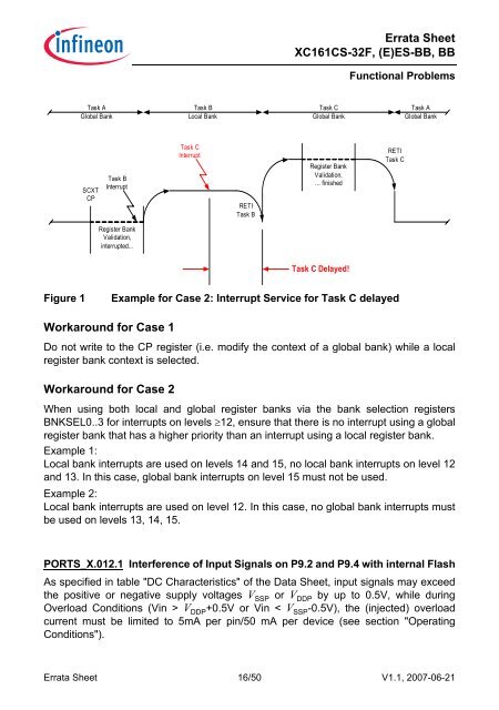
Task A<br />
Global Bank<br />
Task B<br />
Local Bank<br />
Task C<br />
Global Bank<br />
Task A<br />
Global Bank<br />
SCXT<br />
CP<br />
Task B<br />
Interrupt<br />
Task C<br />
Interrupt<br />
RETI<br />
Task B<br />
Register Bank<br />
Validation,<br />
… finished<br />
RETI<br />
Task C<br />
Register Bank<br />
Validation,<br />
interrupted...<br />
Task C Delayed!<br />
Figure 1<br />
Example for Case 2: Interrupt Service for Task C delayed<br />
Workaround for Case 1<br />
Do not write to the CP register (i.e. modify the context of a global bank) while a local<br />
register bank context is selected.<br />
Workaround for Case 2<br />
When using both local and global register banks via the bank selection registers<br />
BNKSEL0..3 for interrupts on levels ≥12, ensure that there is no interrupt using a global<br />
register bank that has a higher priority than an interrupt using a local register bank.<br />
Example 1:<br />
Local bank interrupts are used on levels 14 and 15, no local bank interrupts on level 12<br />
and 13. In this case, global bank interrupts on level 15 must not be used.<br />
Example 2:<br />
Local bank interrupts are used on level 12. In this case, no global bank interrupts must<br />
be used on levels 13, 14, 15.<br />
PORTS_X.012.1 Interference of Input Signals on P9.2 and P9.4 with internal Flash<br />
As specified in table "DC Characteristics" of the Data <strong>Sheet</strong>, input signals may exceed<br />
the positive or negative supply voltages V SSP or V DDP by up to 0.5V, while during<br />
Overload Conditions (Vin > V DDP +0.5V or Vin < V SSP -0.5V), the (injected) overload<br />
current must be limited to 5mA per pin/50 mA per device (see section "Operating<br />
Conditions").<br />
<strong>Errata</strong> <strong>Sheet</strong> 16/50 V1.1, 2007-06-21