Low Cost, Dual-Channel, 15V Pin Electronics Driver ... - Semtech
Low Cost, Dual-Channel, 15V Pin Electronics Driver ... - Semtech
Low Cost, Dual-Channel, 15V Pin Electronics Driver ... - Semtech

Create successful ePaper yourself
Turn your PDF publications into a flip-book with our unique Google optimized e-Paper software.
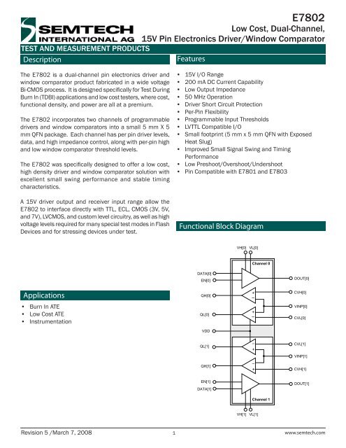
E7802<br />
<strong>Low</strong> <strong>Cost</strong>, <strong>Dual</strong>-<strong>Channel</strong>,<br />
<strong>15V</strong> <strong>Pin</strong> <strong>Electronics</strong> <strong>Driver</strong>/Window Comparator<br />
TEST AND MEASUREMENT PRODUCTS<br />
Description<br />
Features<br />
The E7802 is a dual-channel pin electronics driver and<br />
window comparator product fabricated in a wide voltage<br />
Bi-CMOS process. It is designed specifically for Test During<br />
Burn In (TDBI) applications and low cost testers, where cost,<br />
functional density, and power are all at a premium.<br />
The E7802 incorporates two channels of programmable<br />
drivers and window comparators into a small 5 mm X 5<br />
mm QFN package. Each channel has per pin driver levels,<br />
data, and high impedance control, along with per-pin high<br />
and low window comparator threshold levels.<br />
The E7802 was specifically designed to offer a low cost,<br />
high density driver and window comparator solution with<br />
excellent small swing performance and stable timing<br />
characteristics.<br />
A <strong>15V</strong> driver output and receiver input range allow the<br />
E7802 to interface directly with TTL, ECL, CMOS (3V, 5V,<br />
and 7V), LVCMOS, and custom level circuitry, as well as high<br />
voltage levels required for many special test modes in Flash<br />
Devices and for stressing devices under test.<br />
• <strong>15V</strong> I/O Range<br />
• 200 mA DC Current Capability<br />
• <strong>Low</strong> Output Impedance<br />
• 50 MHz Operation<br />
• <strong>Driver</strong> Short Circuit Protection<br />
• Per-<strong>Pin</strong> Flexibility<br />
• Programmable Input Thresholds<br />
• LVTTL Compatible I/O<br />
• Small footprint (5 mm x 5 mm QFN with Exposed<br />
Heat Slug)<br />
• Improved Small Signal Swing and Timing<br />
Performance<br />
• <strong>Low</strong> Preshoot/Overshoot/Undershoot<br />
• <strong>Pin</strong> Compatible with E7801 and E7803<br />
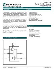
Functional Block Diagram<br />
VH[0]<br />
VL[0]<br />
<strong>Channel</strong> 0<br />
DATA[0]<br />
EN[0]<br />
DOUT[0]<br />
Applications<br />
• Burn In ATE<br />
• <strong>Low</strong> <strong>Cost</strong> ATE<br />
• Instrumentation<br />
QH[0]<br />
QL[0]<br />
VDD<br />
CVH[0]<br />
VINP[0]<br />
CVL[0]<br />
QL[1]<br />
CVL[1]<br />
VINP[1]<br />
QH[1]<br />
CVH[1]<br />
EN[1]<br />
DATA[1]<br />
DOUT[1]<br />
<strong>Channel</strong> 1<br />
VH[1]<br />
VL[1]<br />
Revision 5 /March 7, 2008<br />
<br />
www.semtech.com
E7802<br />
TEST AND MEASUREMENT PRODUCTS<br />
PIN Description<br />
Customer <strong>Pin</strong> Descriptions<br />
<strong>Pin</strong> Name <strong>Pin</strong> Number Description<br />
DATA[0:1] 30, 11 Digital inputs which determine the high/low output state of the driver, when it is<br />
enabled.<br />
EN[0:1] 29, 12 Digital input which enables/disables the driver.<br />
QH[0:1]<br />
QL[0:1]<br />
32, 9<br />
31, 10<br />
Comparator digital outputs.<br />
DOUT[0:1] 22, 19 <strong>Driver</strong> Outputs.<br />
VINP[0:1] 24, 17 Comparator Inputs.<br />
VH[0:1] 23, 18 Unbuffered analog inputs that set the driver high voltage level.<br />
VL[0:1]) 21, 20 Unbuffered analog inputs that set the driver low voltage level.<br />
CVH[0:1] 27, 14 Analog inputs that set the threshold for the high comparator.<br />
CVL[0:1] 25, 16 Analog inputs that set the threshold for the low comparator.<br />
VDD 2, 3 Digital supply.<br />
GND 7 Ground pad. Connect to 0V.<br />
VCC[0:1] 28, 13 Positive power supply.<br />
VEE 4, 5, Center Pad Negative power supply.<br />
DVEE[0:1] 26, 15 <strong>Driver</strong> negative supply.<br />
SCP* 1 Short circuit protection enable pin (has 5.3Kohms internal pull-down to GND).<br />
Connect to VDD if short circuit protection is not required in the application.<br />
INT* 6 Open drain short circuit flag that pulls-down to indicate that a channel of the<br />
E7802 is in short circuit protection mode.<br />
TEMP 8 Connected to anode of temperature sensing diodes.<br />
© 2008 <strong>Semtech</strong> Corp. , Rev. 5, 3/7/08<br />
<br />
www.semtech.com
E7802<br />
TEST AND MEASUREMENT PRODUCTS<br />
PIN Description (continued)<br />
<strong>Pin</strong>out<br />
QH[0]<br />
QL[0]<br />
DATA[0]<br />
EN[0]<br />
VCC[0]<br />
CVH[0]<br />
DVEE[0]<br />
CVL[0]<br />
SCP*<br />
1<br />
VINP[1]<br />
VDD<br />
2<br />
VH[0]<br />
VDD<br />
VEE<br />
VEE<br />
INT*<br />
3<br />
4<br />
5<br />
6<br />
DOUT[0]<br />
VL[0]<br />
VL[1]<br />
DOUT[1]<br />
GND<br />
7<br />
VH[1]<br />
TEMP<br />
8<br />
VINP[1]<br />
QH[1]<br />
QL[1]<br />
DATA[1]<br />
EN[1]<br />
VCC[1]<br />
CVH[1]<br />
DVEE[1]<br />
CVL[1]<br />
9<br />
10<br />
11<br />
12<br />
13<br />
14<br />
15<br />
16<br />
32<br />
31<br />
30<br />
29<br />
28<br />
27<br />
26<br />
25<br />
24<br />
23<br />
32-Pad<br />
5mm X 5mm<br />
MLP with<br />
Exposed Thermal Pad<br />
(Connect to VEE)<br />
22<br />
21<br />
20<br />
19<br />
18<br />
17<br />
© 2008 <strong>Semtech</strong> Corp. , Rev. 5, 3/7/08<br />
<br />
www.semtech.com
E7802<br />
TEST AND MEASUREMENT PRODUCTS<br />
Circuit Description<br />
Description<br />
The E7802 supports independently programmable driver<br />
high and low levels as well as tristate per channel. There<br />
are no shared lines between the two drivers. The EN and<br />
DATA signals are inputs that are used to control the output<br />
of the driver as shown in Table 1. Each channel of the<br />
E7802 features a window comparator with separate high<br />
and low threshold levels (CVH, CVL), as well as independent<br />
digital outputs (QH, QL).<br />
EN DATA DOUT<br />
0 0 HiZ<br />
0 1 HiZ<br />
1 0 VL<br />
1 1 VH<br />
Table 1. <strong>Driver</strong> Functionality<br />
NOTE: The voltage at DOUT needs to stay at DVEE < DOUT<br />
< VCC at all times (HiZ/Active).<br />
Drive High and <strong>Low</strong><br />
<strong>Driver</strong> Output Protection<br />
The E7802’s drivers feature short circuit protection circuitry<br />
that prevents them from being damaged in the event of a<br />
short circuit at their outputs. In the event of a short circuit<br />
at the driver output and short circuit protection is enabled<br />
(SCP*=0), DOUT will place itself in a high impedance state<br />
and the comparator outputs, QH and QL, are designed to<br />
both assert a Logic “0” to indicate that a short circuit event<br />
has occurred. In addition to the comparator outputs pulling<br />
down, the INT* pin will become active (pull-down) when<br />
either channel detects a s hort-circuit condition. Multiple<br />
E7802 INT* pins may be wire-or’d together with a single<br />
VDD pull-up load to create a system-wide notification signal<br />
that a short circuit has occurred on one of the chanels in<br />
the system. After a short circuit event has occurred, the<br />
driver can be reset to the active state by toggling the EN<br />
pin from Logic “0” to Logic “1” .<br />
Either after power-up or after short circuit protection is<br />
enabled, the EN pin needs to be toggled from Logic “0” to<br />
Logic “1” to allow the driver to power up in the active state<br />
and ensure the short circuit protection is reset for proper<br />
operation (see Timing Diagram below).<br />
short circuit occurs<br />
VH and VL define the logical “1” and “0” levels of the driver,<br />
and can be adjusted to produce driver output swings from<br />
200mV up to <strong>15V</strong>.<br />
DOUT<br />
QH<br />
Valid Comp. Output<br />
Tri-state<br />
The VH and VL inputs are unbuffered. They provide the<br />
driver output current (see Figure 1), so the source of VH<br />
and VL must have ample current drive capability. (See<br />
Applications Note PE-A1).<br />
QL<br />
INT*<br />
Valid Comp. Output<br />
VH<br />
EN<br />
DATA<br />
EN<br />
<strong>Driver</strong> Logic<br />
VL<br />
DOUT<br />
T INT*<br />
Because of the nature of the SCP circuit design, it is<br />
recommended that the user have SCP enabled only under<br />
the valid SCP operating zone. Refer to Figure 2 for the<br />
conditions.<br />
Toe<br />
Figure 1.<br />
© 2008 <strong>Semtech</strong> Corp. , Rev. 5, 3/7/08<br />
<br />
www.semtech.com
E7802<br />
TEST AND MEASUREMENT PRODUCTS<br />
Circuit Description (continued)<br />
VH [V] (VL=0V)<br />
Short Circuit Protection Operating Zone<br />
16<br />
14<br />
12<br />
10<br />
8<br />
6<br />
Tj=100C<br />
Tj=65C<br />
Tj=40C<br />
Tj=25C<br />
6. Disable short circuit protection (SCP*=1) and<br />
start running the driver at the desired operating<br />
conditions.<br />
NOTE: If short circuit protection is used outside of the valid<br />
SCP operating zone, false SCP triggers can occur which will<br />
disable the driver output, DOUT.<br />
4<br />
2<br />
Valid SCP<br />
Operating Zone<br />
0<br />
0 5 10 15 20 25 30 35 40 45 50<br />
Freq (MHz)<br />
Figure 2.<br />
For applications that require operation outside the valid<br />
SCP operating zone, the user can use the SCP to check<br />
for any short circuit occurrence down the line and protect<br />
the driver from over-current damage before running it at<br />
the desired operating conditions. Refer to the following<br />
procedure:<br />
1. While the driver is in HiZ (EN=0), enable short-circuit<br />
protection (SCP*=0)<br />
2. Set VH to the maximum programmable voltage in the<br />
system, switch DATA to Logic “1” and toggle the EN<br />
pin from Logic “0” to “Logic “1”.<br />
3. After the driver is enabled, wait approximately 2 µs<br />
and monitor all INT* pins in the system to determine<br />
if there is any short circuit occurrence.<br />
4. If the INT* signal remains high, no short circuit<br />
condition is detected. If the INT* signal becomes<br />
low (active), this indicates a short circuit condition<br />
has occurred in one or more channels in the system.<br />
Determine the shorted channel(s) by checking the<br />
comparator outputs (QH=0, QL=0). Remove the fault<br />
condition in each channel respectively and reset those<br />
driver(s)<br />
5. Repeat Steps 3 through 4 with minimum programmable<br />
VL in the system and switch DATA to Logic “0”.<br />
Window Comparator<br />
CVH<br />
VINP<br />
CVL<br />
+<br />
+<br />
Each channel of the E7802 features two comparators<br />
connected in a window comparator configuration. CVH<br />
and CVL are high impedance analog voltage inputs that<br />
establish the upper and lower thresholds for the window<br />
comparator. CVH should always be greater than or equal<br />
to CVL for normal comparator operation. QH and QL are<br />
digital outputs that indicate where a voltage measurement<br />
lies in relation to the CVH and CVL thresholds and are also<br />
used to indicate when short circuit protection is engaged<br />
as shown in Table 2.<br />
QH<br />
QL<br />
Condition QH QL INT*<br />
Measurement is within the range<br />
established by CVH and CVL<br />
Measurement is above the range<br />
established by CVH and CVL<br />
Measurement is below the range<br />
established by CVH and CVL<br />
Short circuit protection is engaged<br />
and <strong>Driver</strong> is disabled<br />
1 1 1<br />
0 1 1<br />
1 0 1<br />
0 0 0<br />
Table 2. Comparator Output Truth Table<br />
The receiver thresholds can be used over a range of VEE<br />
+3V to VCC -3V. The VINP input of the receiver is designed<br />
to withstand voltages from VEE+2V to VCC such that the<br />
comparator input can be directly connected to the driver<br />
output without being damaged.<br />
© 2008 <strong>Semtech</strong> Corp. , Rev. 5, 3/7/08<br />
<br />
www.semtech.com
E7802<br />
TEST AND MEASUREMENT PRODUCTS<br />
Circuit Description (continued)<br />
NOTE: DVEE MUST be set appropriately in order to<br />
accommodate VINP input voltages of VEE + 2V when DOUT<br />
and VINP are connected in an application.<br />
Thermal Diode String<br />
The E7802 features an internal diode string connected<br />
between EN[1] and TEMP that can be used to perform<br />
device junction temperature measurements as shown in<br />
the figure below. NOTE: EN[1] must be asserted “low”<br />
when making temperature measurements.<br />
EN[1]<br />
100 µA<br />
External<br />
Current<br />
Source<br />
Temperature<br />
Coefficient= –5.9mV/°C<br />
TEMP<br />
(0.7195 – TEMP – EN[1] )<br />
3<br />
Tj[°C] =<br />
0.001967<br />
© 2008 <strong>Semtech</strong> Corp. , Rev. 5, 3/7/08<br />
<br />
www.semtech.com
E7802<br />
TEST AND MEASUREMENT PRODUCTS<br />
Application Information<br />
Power Supply Decoupling<br />
VCC, VEE, and DVEE should be decoupled to GND with a .1<br />
µF chip capacitor in parallel with a .001 µF chip capacitor<br />
for best AC performance. A VCC, VEE, and DVEE plane, or<br />
at least a solid power bus, is recommended for optimal<br />
performance.<br />
The three diode configuration shown in Figure 3 should be<br />
used on a once-per-boad basis to help ensure that proper<br />
supply polarities are maintained.<br />
VCC<br />
VH and VL Inputs<br />
As the VH and VL inputs are unbuffered to the driver and<br />
need to supply the output current which can be quite large<br />
during edge transitions, bypass capacitors for these inputs<br />
are needed to supply the transient currents in proportion<br />
to the output current requirements (See Applications Note<br />
PE-A1).<br />
For applications where VH and VL are shared over multiple<br />
channels, a solid power plane to distribute these levels with<br />
local bypassing is recommended for best AC performance<br />
.<br />
Power Supply Sequencing/Latch-Up Protection<br />
In order to avoid the possibility of latch-up when powering<br />
this device up (or down), be careful that the conditions<br />
listed in the Absolute Maximum Ratings are never violated.<br />
The power supplies should never be in reverse-polarity with<br />
respect to ground, and the input signals should never go<br />
beyond the power supply rails.<br />
Furthermore, the lower-voltage supplies should never be<br />
greater than the higher-voltage supplies. This can easily<br />
be implemented by utilizing the diode circuit depicted in<br />
Figure 3 for each PCB utilizing the E7802. The following<br />
conditions must be met at all times during power-up and<br />
power-down:<br />
1. VEE
E7802<br />
TEST AND MEASUREMENT PRODUCTS<br />
Application Information (continued)<br />
Cooling Considerations<br />
Depending on the maximum operating frequencies and<br />
voltage swings the E7802 will need to drive, it may require<br />
the use of an external heatsink to keep the maximum die<br />
junction temperature within a safe range and below the<br />
specified maximum of 100°C.<br />
The E7802 package has an external heat slug located on<br />
the bottom side of the package to efficiently conduct heat<br />
away from the die to the package surface. The thermal<br />
resistance of the package to the slug is the θjc (junctionto-case)<br />
and is specified at
E7802<br />
TEST AND MEASUREMENT PRODUCTS<br />
Application Information (continued)<br />
External "<strong>Driver</strong> High" Buffer<br />
Therefore, the per-channel power dissipation due to the<br />
E7802 driving resistive load is:<br />
Simplified<br />
E7802<br />
Output<br />
Stage<br />
VH<br />
Rds(H)<br />
H<br />
L<br />
Rds(L)<br />
VL<br />
DOUT IL<br />
RT<br />
VT<br />
P = [I L<br />
2<br />
(H) x R ds(H) x D] + [I L<br />
2<br />
(L)] x R ds(L) x (1–D)]<br />
where:<br />
P is the total power dissipated by E7802 as<br />
a result of the resistive load, R L [Ω]<br />
I L(H) is the amount of current required by R L<br />
during a logic “high” state [A]<br />
R ds(H) is the output impedance of the E7802<br />
driver when driving a logic “high” state [Ω]<br />
D is the normalized amount of time that logic<br />
“high” is driven (Duty Cycle)<br />
I L(L) is the amount of current required by R L<br />
during a logic “low” state [A]<br />
R ds(L) is the output impedance of the E7802<br />
driver when driving a logic “low” state [Ω]<br />
External "<strong>Driver</strong> <strong>Low</strong>" Buffer<br />
Figure 4. Simplified Functional Schematic of E7802<br />
Output Stage and External Buffers<br />
The CMOS switches of the E7802’s output stage have onresistance<br />
values (depicted by R ds(H) and R ds(L) in Figure<br />
4) that vary as a function of VH and VL voltage levels. The<br />
amount of current required by the load impedance, R T , is<br />
also a function of the VH and VL voltage levels as follows:<br />
Driving Currents Larger than 200mA<br />
The driver channels of the E7802 can be connected in<br />
parallel to drive currents larger than the rated 200mA per<br />
individual driver.<br />
Switch in Figure 3 is in position “H”:<br />
I L(H) =<br />
Switch in Figure3 is in position “L”:<br />
I L(L) =<br />
VH – V T<br />
R ds(H) + R T<br />
VL – V T<br />
R ds(L) + R T<br />
© 2008 <strong>Semtech</strong> Corp. , Rev. 5, 3/7/08<br />
<br />
www.semtech.com
E7802<br />
TEST AND MEASUREMENT PRODUCTS<br />
Application Information (continued)<br />
Optimizing <strong>Driver</strong> Waveforms<br />
Overshoot/Undershoot/Preshoot<br />
E7802 <strong>Driver</strong> overshoot, undershoot and preshoot are<br />
functions of the DOUT edge rate. Slower DOUT edge rates<br />
are associated with smaller overshoot, undershoot and<br />
preshoot amplitudes. The DOUT edge rate is influenced<br />
by the amount of capacitance that is present on the driver<br />
output with larger capacitance resulting in slower edge<br />
rates and less overshoot as shown below.<br />
<strong>Driver</strong> Output Waveform vs. Capacitive Load<br />
matching for a 50Ω transmission line. See<br />
Applications Note PE-A2, “Optimizing the Output<br />
Configuration of <strong>Semtech</strong> Bipolar <strong>Pin</strong> <strong>Driver</strong>s” for<br />
more details on selecting the proper “back-match”<br />
resistor.<br />
2) Reactive Component: Accounts for the reactive<br />
or “AC” component of the output impedance and<br />
is matched to a transmission line by using external<br />
inductors and/or capacitors. Using empirical<br />
methods in our lab, we have determined that an<br />
18nH series inductor offers the best impedance<br />
matching for a 50Ω transmission line (see below).<br />
3.0<br />
2.5<br />
C = 0pf<br />
2.0<br />
Output Voltage [V]<br />
1.5<br />
1.0<br />
C = 33pF<br />
3.5<br />
3.0<br />
<strong>Driver</strong> Output Impedance Optimization (Reactive Component)<br />
0.5<br />
0.0<br />
-0.5<br />
0 10 20 30 40 50 60 70<br />
Time [nS]<br />
Output Voltage [V]<br />
2.5<br />
2.0<br />
1.5<br />
1.0<br />
0.5<br />
0.0<br />
Overshoot, undershoot and preshoot are also influenced<br />
by power supply levels. In general, lower VCC levels are<br />
associated with less overshoot and better small-swing<br />
performance.<br />
-0.5<br />
0<br />
10<br />
20<br />
30<br />
40<br />
50<br />
Time [ns]<br />
60<br />
70<br />
80<br />
90<br />
Output Impedance Matching<br />
How well the driver output impedance matches a<br />
transmission line connected to it has a direct effect on<br />
waveform characteristics. <strong>Driver</strong> output impedance can<br />
be separated into two components:<br />
1) Real Component: Accounts for the resistive (DC)<br />
portion of the driver output impedance and is<br />
matched to a transmission line by using an external<br />
“back-match” resistor. Using empirical methods in<br />
our lab, we have determined that a 45.3Ω backmatch<br />
resistor offers the best real impedance<br />
L = 18nH<br />
External component connections are illustrated in the<br />
E7802 Hookup Diagram.<br />
© 2008 <strong>Semtech</strong> Corp. , Rev. 5, 3/7/08<br />
10<br />
www.semtech.com
E7802<br />
TEST AND MEASUREMENT PRODUCTS<br />
Application Information (continued)<br />
E7802 Hookup Diagram<br />
VCC DVEE (Note 2)<br />
VDD<br />
1<br />
2<br />
3<br />
SCP*<br />
VDD<br />
VDD<br />
VINP[0]<br />
VH[0]<br />
DOUT[0]<br />
24<br />
23<br />
22<br />
**<br />
45.3Ω<br />
VH<br />
50Ω<br />
18nH<br />
D<br />
U<br />
T<br />
VEE<br />
4<br />
VEE<br />
VL[0]<br />
21<br />
**<br />
VL<br />
VDD<br />
Rpu<br />
Note 3<br />
5<br />
6<br />
VEE<br />
INT*<br />
VL[1]<br />
DOUT[1]<br />
20<br />
19<br />
**<br />
45.3Ω<br />
VL<br />
7<br />
8<br />
GND<br />
TEMP<br />
VH[1]<br />
VINP[1]<br />
18<br />
17<br />
**<br />
VH<br />
18nH<br />
50Ω<br />
D<br />
U<br />
T<br />
VCC<br />
DVEE<br />
Note 1: All capacitors are 0.1µF unless otherwise noted.<br />
** See Applications Note PE-A1 for proper capacitor and VH/VL supply selection.<br />
Note 2: DVEE supply can be connected to GND if DOUT does not need to swing below 0V.<br />
Note 3: Choose Rpu such that the INT* current is less than 5mA.<br />
© 2008 <strong>Semtech</strong> Corp. , Rev. 5, 3/7/08<br />
11<br />
www.semtech.com
E7802<br />
TEST AND MEASUREMENT PRODUCTS<br />
Package Information<br />
32-Pad<br />
5mm x 5mm QFN<br />
Package Outline<br />
A<br />
A<br />
PIN 1<br />
INDICATOR<br />
(LASER MARK)<br />
D<br />
B<br />
E<br />
A2<br />
SEATING<br />
DIM<br />
A<br />
A1<br />
A2<br />
b<br />
D<br />
D1<br />
E<br />
E1<br />
e<br />
L<br />
N<br />
aaa<br />
bbb<br />
MIN<br />
INCHES<br />
NOM<br />
-<br />
DIMENSIONS<br />
MAX<br />
MIN<br />
MILLIMETERS<br />
NOM<br />
-<br />
MAX<br />
.031 .039 0.80 1.00<br />
.000 - .002 0.00<br />
-<br />
0.05<br />
- (.008) - - (0.20) -<br />
.007 .010 .012 0.18 0.25 0.30<br />
.193 .197 .201 4.90 5.00 5.10<br />
.130 .136 .140 3.30 3.45 3.55<br />
.193 .197 .201 4.90 5.00 5.10<br />
.130 .136 .140 3.30 3.45 3.55<br />
.020 BSC 0.50 BSC<br />
.012 .016 .020 0.30 0.40 0.50<br />
32<br />
32<br />
.003<br />
0.08<br />
.004<br />
0.10<br />
aaa<br />
C<br />
PLANE<br />
A1<br />
C<br />
D1<br />
LxN<br />
E/2<br />
E1<br />
2<br />
1<br />
N<br />
bxN<br />
e<br />
bbb C A B<br />
NOTES:<br />
D/2<br />
1.<br />
2.<br />
CONTROLLING DIMENSIONS ARE IN MILLIMETERS (ANGLES IN DEGREES).<br />
COPLANARITY APPLIES TO THE EXPOSED PAD AS WELL AS THE TERMINALS.<br />
© 2008 <strong>Semtech</strong> Corp. , Rev. 5, 3/7/08<br />
12<br />
www.semtech.com
E7802<br />
TEST AND MEASUREMENT PRODUCTS<br />
Package Information (continued)<br />
32-Pad<br />
5mm x 5mm QFN<br />
Land Pattern<br />
K<br />
DIMENSIONS<br />
(C)<br />
H<br />
X<br />
P<br />
G<br />
Y<br />
Z<br />
DIM<br />
C<br />
G<br />
H<br />
K<br />
P<br />
X<br />
Y<br />
Z<br />
INCHES<br />
(.197)<br />
.165<br />
.146<br />
.146<br />
.020<br />
.012<br />
.031<br />
.228<br />
MILLIMETERS<br />
(5.00)<br />
4.20<br />
3.70<br />
3.70<br />
0.50<br />
0.30<br />
0.80<br />
5.80<br />
NOTES:<br />
1. CONTROLLING DIMENSIONS ARE IN MILLIMETERS (ANGLES IN DEGREES).<br />
2. THIS LAND PATTERN IS FOR REFERENCE PURPOSES ONLY.<br />
CONSULT YOUR MANUFACTURING GROUP TO ENSURE YOUR<br />
COMPANY'S MANUFACTURING GUIDELINES ARE MET.<br />
3. THERMAL VIAS IN THE LAND PATTERN OF THE EXPOSED PAD<br />
SHALL BE CONNECTED TO A SYSTEM GROUND PLANE.<br />
FAILURE TO DO SO MAY COMPROMISE THE THERMAL AND/OR<br />
FUNCTIONAL PERFORMANCE OF THE DEVICE.<br />
4. SQUARE PACKAGE - DIMENSIONS APPLY IN BOTH " X " AND " Y " DIRECTIONS.<br />
© 2008 <strong>Semtech</strong> Corp. , Rev. 5, 3/7/08<br />
13<br />
www.semtech.com
E7802<br />
TEST AND MEASUREMENT PRODUCTS<br />
Absolute Maximum Ratings<br />
Parameter Symbol Min Max Units<br />
Positive Analog Supply VCC -0.5 DVEE + 16 V<br />
Negative Analog Supply VEE -6 +0.5 V<br />
Negative <strong>Driver</strong> Supply DVEE VEE +0.5 V<br />
Digital Power Supply VDD -0.5 +6.0 V<br />
Digital Input Voltages EN[0:1], DATA[0:1], SCP* -0.5 VDD + 0.5 V<br />
<strong>Driver</strong> <strong>Pin</strong>s VH[0:1], VL[0:1], DOUT[0:1] DVEE + 0.5 VCC + 0.5 V<br />
Comparator <strong>Pin</strong>s CVH[0:1], CVL[0:1], VINP[0:1] VEE - 0.5 VCC + 0.5 V<br />
Storage Temperature TS -65 +150 °C<br />
Junction Temperature Tj +150 °C<br />
IR Reflow Conditions Tpkg +260 °C<br />
Recommended Operating Conditions<br />
Parameter Symbol Min Typ Max Units<br />
Positive Analog Supply VCC DVEE + 9 DVEE + 14.5 DVEE + 15 V<br />
Negative Analog Supply VEE -5.25 -5 -4.75 V<br />
Negative <strong>Driver</strong> Supply DVEE -3.6 0 V<br />
Digital Power Supply VDD 3.0 3.6 V<br />
Thermal Resistance - Junction to Case θjc<br />
Junction to Top-Center of Case 4 °C/W<br />
Junction to Bottom-Center of Heat Slug 1 °C/W<br />
Thermal Resistance - Junction to Ambient Still Air θja 26 °C/W<br />
Junction Temperature TJ 25 100 °C<br />
Stresses above those listed in “Absolute Maximum Ratings” section may cause permanent damage to the device.<br />
This is a stress rating only, and functional operation of the device at these, or any other conditions beyond<br />
those listed, is not implied. Exposure to absolute maximum conditions for extended periods may affect device<br />
reliability.<br />
© 2008 <strong>Semtech</strong> Corp. , Rev. 5, 3/7/08<br />
14<br />
www.semtech.com
E7802<br />
TEST AND MEASUREMENT PRODUCTS<br />
DC Characteristics<br />
Parameter Symbol Min Typ Max Units<br />
<strong>Driver</strong><br />
<strong>Driver</strong> "High Level" Range VH VL VCC V<br />
<strong>Driver</strong> "<strong>Low</strong> Level" Range VL<br />
10.4 V < VCC ≤ <strong>15V</strong> DVEE VCC - 8.4 V<br />
5.4V ≤ VCC ≤ 10.4V DVEE 2 V<br />
<strong>Driver</strong> Output Swing DOUT 0.2 15 V<br />
<strong>Driver</strong> Output Impedance Rout<br />
VCC = <strong>15V</strong>, Tj = 65°C ± 3°C 4 8.5 Ω<br />
Across Recommended Operating Conditions 2.5 11 Ω<br />
Offset Voltage |VH, VL - DOUT| 0.5 2.5 mV<br />
<strong>Driver</strong> Digital Input Logic Levels (DATA, EN, SCP*)<br />
Logic Input "High" Level VIH 2.0 V<br />
Logic Input "<strong>Low</strong>" Level VIL 0.8 V<br />
<strong>Driver</strong> Digital Input Current<br />
DATA, EN IIH, IIL -200 +200 nA<br />
SCP* IIH, IIL -1 0 mA<br />
Hi-Z Leakage Current at DOUT (DVEE ≤ DOUT ≤ VCC) ILEAK -35 +75 nA<br />
DC Output Current (Note 1) IOUT(DC) -200 +200 mA<br />
AC Output Current (Note 2) IOUT(AC) ±1.4 ±3.6 A<br />
Short Circuit Protection Threshold<br />
VL ≤ DOUT ≤ VH 205 300 mA<br />
DVEE ≤ DOUT ≤ VCC 75 350 mA<br />
INT* Output <strong>Low</strong> Voltage @ I INT *=5mA VOL 0.4 V<br />
Comparator<br />
Analog Inputs<br />
CVH Input Voltage Range (Note 3) VCVH VCVL VCC - 3 V<br />
CVL Input Voltage Range (Note 3) VCVL VEE + 3 VCVH V<br />
CVH, CVL Input Current IIN -15 +15 µA<br />
VINP Voltage Range V VINP VEE + 2 VCC V<br />
VINP Input Current<br />
I VINP<br />
DVEE ≤ VINP ≤ VCC - 3V -30 +30 µA<br />
Across Full VINP Range -200 +200 µA<br />
Hysteresis VHYS 30 mV<br />
Offset Voltage VOS -50 +50 mV<br />
Digital Outputs<br />
Output "High" Voltage @ +5 mA VOH 2.4 V<br />
Output "<strong>Low</strong>" Voltage @ -5 mA VOL 0.4 V<br />
Test conditions (unless otherwise specified): “Recommended Operating Conditions”.<br />
Note 1: DC output current is specified per individual driver, V VL < V DOUT < V VH .<br />
Note 2: Surge current capability with 1000pF lumped capacitive load on DOUT defined as the maximum<br />
output current during a <strong>15V</strong> step.<br />
Note 3: Comparator threshold inputs (CVH, CVL) can be overlapped (i.e. VCVH < VCVL), but comparator output<br />
logic will be inverted and functionality of the comparators is not guaranteed under this condition.<br />
© 2008 <strong>Semtech</strong> Corp. , Rev. 5, 3/7/08<br />
15<br />
www.semtech.com
E7802<br />
TEST AND MEASUREMENT PRODUCTS<br />
DC Characteristics (continued)<br />
Parameter Symbol Min Typ Max Units<br />
Power Supply Current (Quiescent)<br />
Positive Supply Current ICC 11 24 40 mA<br />
<strong>Driver</strong> Negative Supply Current IDEE 1.5 7 12 mA<br />
Negative Supply Current IEE 11 16 26 mA<br />
Digital Supply Current IDD 2 6 14 mA<br />
© 2008 <strong>Semtech</strong> Corp. , Rev. 5, 3/7/08<br />
16<br />
www.semtech.com
E7802<br />
TEST AND MEASUREMENT PRODUCTS<br />
AC Characteristics<br />
Parameter Symbol Min Typ Max Units<br />
<strong>Driver</strong> (Note 1)<br />
Propagation Delay<br />
DATA to DOUT (Figure 5) Tpd 13.6 15.6 ns<br />
EN to DOUT (Active to HiZ) (Figure 7) Tz 8 17 ns<br />
EN to DOUT (HiZ to Active) (Figure 7) Toe 8 14 ns<br />
Propagation Delay Matching |Tpd+ - Tpd-| 1 ns<br />
Propagation Delay Tempco (∆Tj = 25°C to 100°C) ∆Tpd/∆T 30 ps/°C<br />
<strong>Driver</strong> Propagation Delay Dispersion ∆Tpd(swing) 1 ns<br />
vs. Amplitude (VL = 0, 0.2 < VH < 3.0)<br />
Short Circuit Protection Activation Time<br />
Pulse Width for Trigger (VH=3V, VL=0V, DOUT Shorted to 0V) Tprotect 125 ns<br />
Short to Comparator Trigger Tpd 600 ns<br />
Short to INT* Trigger T INT* 600 ns<br />
Rise/Fall Times (1000pF lumped capacitance at DOUT, Figure 5a)<br />
3V Programmed Swing (10% - 90%) Tr/Tf 9.5 16 ns<br />
5V Programmed Swing (10% - 90%) Tr/Tf 10 16 ns<br />
Rise/Fall Times (100pF Lumped Capacitance at DOUT, Figure 5a)<br />
0.4V Programmed Swing (20% - 80%) (Note 8) Tr/Tf 2 4 ns<br />
1V Programmed Swing (20% - 80%) Tr/Tf 3 5 ns<br />
3V Programmed Swing (10% - 90%) Tr/Tf 3.5 5.5 ns<br />
5V Programmed Swing (10% - 90%) Tr/Tf 4 6.5 ns<br />
Rise/Fall Times (50Ω termination, Figure 5b)<br />
0.4V Programmed Swing (20% - 80%) (Note 8) Tr/Tf 2 4 ns<br />
1V Programmed Swing (20% - 80%) Tr/Tf 3 5 ns<br />
3V Programmed Swing (10% - 90%) Tr/Tf 3.5 5.5 ns<br />
5V Programmed Swing (10% - 90%) Tr/Tf 4 6.5 ns<br />
Maximum Operating Frequency (50Ω termination, Figure 5b)<br />
Fmax<br />
0.4V Programmed Swing (Note 8) 50 MHz<br />
1V Programmed Swing 50 MHz<br />
3V Programmed Swing 50 MHz<br />
5V Programmed Swing 50 MHz<br />
Maximum Operating Frequency (1KΩ termination, Figure 5c)<br />
Fmax<br />
0.4V Programmed Swing (Note 8) 50 MHz<br />
1V Programmed Swing 50 MHz<br />
3V Programmed Swing 50 MHz<br />
5V Programmed Swing 50 MHz<br />
<strong>15V</strong> Programmed Swing 50 MHz<br />
DOUT Capacitance CDOUT 50 pF<br />
<strong>Driver</strong> Overshoot/Preshoot/Undershoot (3V)<br />
(1KΩ termination, Figures 5c, 13, Note 6)<br />
Vovershoot 100 mV<br />
Minimum Pulse Width (Figures 5b, 9)<br />
Mpw<br />
0.4V Programmed Swing (Note 8) 7 ns<br />
1V Programmed Swing 7.5 ns<br />
3V Programmed Swing 8 ns<br />
5V Programmed Swing 9 ns<br />
© 2008 <strong>Semtech</strong> Corp. , Rev. 5, 3/7/08<br />
17<br />
www.semtech.com
E7802<br />
TEST AND MEASUREMENT PRODUCTS<br />
AC Characteristics (continued)<br />
Parameter Symbol Min Typ Max Units<br />
Comparator (Note 2)<br />
Comparator Propagation Delay (Figure 10, Note 5) Tpd +/- 3.5 5 6.5 ns<br />
Propagation Delay Matching (Note 5) |(Tpd+) - (Tpd-)| 0.5 1.5 ns<br />
Propagation Delay Tempco (∆Tj = 25°C to 100°C) ∆Tpd/∆T 15 20 ps/°C<br />
Propagation Delay Dispersion vs. Overdrive (Note 7) (Figure 11) ∆Tpd/∆(VINP-<br />
VCH(L))<br />
100mV to 1V Overdrive 2.5 3.5 ns<br />
1V to 2.5V Overdrive 0.25 0.5 ns<br />
Propagation Delay Dispersion vs. Common Mode (Figure 12, Notes 3, 7) ∆Tpd(cm) 0.5 ns<br />
Comparator Bandwidth (Note 4) Fmax 100 MHz<br />
Minimum Pulse Width 5 ns<br />
VINP Capacitance CVINP 3 pF<br />
Note 1: <strong>Driver</strong> AC specifications are with Tj = 65 o C ± 3 o C, VCC = <strong>15V</strong>, VDD = 3.3V, DVEE = 0V, VEE = -5V,<br />
VL = 0, VH = 3.0, into 20 inches of 50Ω transmission line unless otherwise noted.<br />
Note 2: Tj = 65 o C ± 3 o C, CVH = 1.5, CVL = 1.5, VINP 0 - 3V @ 10MHz. VCC = <strong>15V</strong>, VDD = 3.3V, DVEE = 0V,<br />
VEE = -5V unless otherwise noted.<br />
Note 3: V VINP = 5V pp, 0.5V < V CVH/L < 1.5V.<br />
Note 4: Comparator bandwidth is the maximum frequency under which the comparator will switch with<br />
CVH/CVL = 1.5V, VINP = 0 to 3V.<br />
Note 5: V VINP = 5Vpp, VCVH,L = 2.5V.<br />
Note 6: Measured with 33pF at end of transmission line. See “Optimizing <strong>Driver</strong> Waveforms” Section for<br />
characteristics with different capacitive loads.<br />
Note 7: CVH, CVL are Calibrated Threshold Values (i.e., “Switching Point”).<br />
Note 8: VCC = 9V, DVEE = 0V, VEE = -5V.<br />
Test Circuits:<br />
Measurement Point (VX)<br />
DOUT<br />
45.3Ω<br />
Measurement Point (VX)<br />
DOUT<br />
VINP<br />
C LOAD<br />
953Ω<br />
Oscilloscope<br />
50 Ω<br />
VINP<br />
18nH<br />
20" T-line<br />
50 Ω<br />
Oscilloscope<br />
50 Ω<br />
Figure 5a. <strong>Driver</strong> Output/Comparator Input, Lumped Load<br />
Figure 5b. <strong>Driver</strong> Output/Comparator Input, 50Ω Load<br />
DOUT<br />
45.3Ω<br />
Measurement Point (VX)<br />
VINP<br />
18nH<br />
20" T-line<br />
50 Ω<br />
953Ω<br />
Oscilloscope<br />
50 Ω<br />
Figure 5c. <strong>Driver</strong> Output/Comparator Input, 1KΩ Load<br />
© 2008 <strong>Semtech</strong> Corp. , Rev. 5, 3/7/08<br />
18<br />
www.semtech.com
E7802<br />
TEST AND MEASUREMENT PRODUCTS<br />
AC Characteristics (continued)<br />
DOUT<br />
50%<br />
Tpd+<br />
Tpd-<br />
DATA<br />
Figure 6. <strong>Driver</strong> Propagation Delay Measurements<br />
DOUT<br />
+0.5V<br />
90%<br />
10%<br />
0.0V<br />
Toe<br />
Tz<br />
Time<br />
EN<br />
Transmission line terminated 50Ω to ground.<br />
Figure 7. <strong>Driver</strong> HiZ Enable/Disable Delay Measurement Definition<br />
Measurement Point (VX)<br />
OUT(H) = 0.4V, 1V, 3V, 5V<br />
OUT(H)<br />
1 / Fmax<br />
0.90 OUT(H)<br />
0.0V<br />
Time<br />
Figure 8. <strong>Driver</strong> Fmax Measurement Definition<br />
© 2008 <strong>Semtech</strong> Corp. , Rev. 5, 3/7/08<br />
19<br />
www.semtech.com
E7802<br />
TEST AND MEASUREMENT PRODUCTS<br />
AC Characteristics (continued)<br />
Measurement Point (VX)<br />
VX High = 0.4V, 1V, 3V, 5V<br />
VX <strong>Low</strong> = 0V<br />
Period = 100ns<br />
VX High<br />
VX <strong>Low</strong> + 0.9 *<br />
(V X High - VX<strong>Low</strong>)<br />
Tpw+<br />
Tpw–<br />
Output<br />
Signal<br />
(V X High +<br />
VX <strong>Low</strong>)/2<br />
VX <strong>Low</strong> + 0.1 *<br />
(V X High - VX <strong>Low</strong>)<br />
VX <strong>Low</strong><br />
Figure 9. <strong>Driver</strong> Minimum Pulse Width Measurement Definition<br />
Time<br />
VINP<br />
100%<br />
SR = 1V/ns<br />
50%<br />
V CVH , V CVL<br />
0%<br />
Comparator Output<br />
QL<br />
50%<br />
Tpd+<br />
Tpd-<br />
Time<br />
QH<br />
50%<br />
Time<br />
Tpd-<br />
Tpd+<br />
Figure 10. Comparator Propagation Delay Measurements<br />
VINP<br />
INPUT: Freq = 10 MHz; 50% Duty Cycle, SR = 1V/ns<br />
20-80% Tr/Tf for 500mV p-p = 0.3ns; for 5V p-p = 3ns<br />
2.5V<br />
100mV<br />
2.5V<br />
CVH/L<br />
100mV<br />
2.5V<br />
0.0V<br />
Time<br />
Comparator Output<br />
Tpd-<br />
Tpd+<br />
QH<br />
50%<br />
Time<br />
QL<br />
50%<br />
Time<br />
Tpd+<br />
Tpd-<br />
Figure 11. Comparator Dispersion: Overdrive Measurement Definition<br />
© 2008 <strong>Semtech</strong> Corp. , Rev. 5, 3/7/08<br />
20<br />
www.semtech.com
E7802<br />
TEST AND MEASUREMENT PRODUCTS<br />
AC Characteristics (continued)<br />
VVINP<br />
INPUT: Freq = 10 MHz<br />
+1.5V<br />
VCVH/L = 50%<br />
+1.0V<br />
VCVH/L = 50%<br />
0.5V<br />
VCVH/L = 50%<br />
Comparator Output<br />
QH<br />
50%<br />
QL<br />
Tpd+<br />
Tpd-<br />
Time<br />
Figure 12. Comparator Dispersion: Common Mode Definition<br />
Figure 13. <strong>Driver</strong> Overshoot, Undershoot, and Ringback<br />
© 2008 <strong>Semtech</strong> Corp. , Rev. 5, 3/7/08<br />
21<br />
www.semtech.com
E7802<br />
TEST AND MEASUREMENT PRODUCTS<br />
Ordering Information<br />
Model Number<br />
Package<br />
E7802ALPT<br />
32-pad, 5mm x 5mm QFN<br />
E7802ALPT-T<br />
32-pad, 5mm x 5mm QFN (Tape & Reel)<br />
EVM7802ALPT<br />
E7802 Evaluation Board<br />
Pb<br />
This product is lead-free.<br />
Contact Information for <strong>Semtech</strong> International AG<br />
Taiwan Branch<br />
Tel: 886-2-2748-3380<br />
Fax: 886-2-2748-3390<br />
<strong>Semtech</strong> Switzerland GmbH<br />
Japan Branch<br />
Tel: 81-3-6408-0950<br />
Fax: 81-3-6408-0951<br />
Korea Branch<br />
Tel: 82-2-527-4377<br />
Fax: 82-2-527-4376<br />
<strong>Semtech</strong> Limited (U.K.)<br />
Tel: 44-1794-527-600<br />
Fax: 44-1794-527-601<br />
Shanghai Office<br />
Tel: 86-21-6391-0830<br />
Fax: 86-21-6391-0831<br />
<strong>Semtech</strong> France SARL<br />
Tel: 33-(0)169-28-22-00<br />
Fax: 33-(0)169-28-12-98<br />
<strong>Semtech</strong> International AG is a wholly-owned subsidiary of<br />
<strong>Semtech</strong> Corporation, which has its headquarters in the U.S.A.<br />
<strong>Semtech</strong> Germany GmbH<br />
Tel: 49-(0)8161-140-123<br />
© 2008 <strong>Semtech</strong> Corp. , Rev. 5, 3/7/08<br />
22<br />
www.semtech.com