ekS - Instytut Agrofizyki im. Bohdana DobrzaÅskiego PAN w Lublinie ...
ekS - Instytut Agrofizyki im. Bohdana DobrzaÅskiego PAN w Lublinie ...
ekS - Instytut Agrofizyki im. Bohdana DobrzaÅskiego PAN w Lublinie ...

Create successful ePaper yourself
Turn your PDF publications into a flip-book with our unique Google optimized e-Paper software.
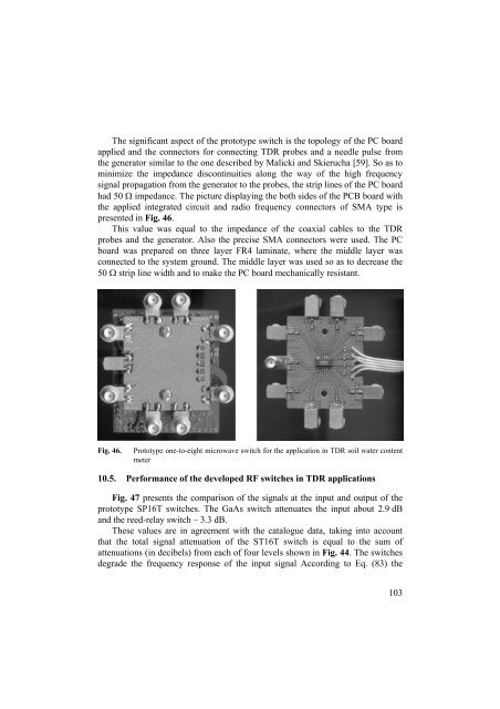
The significant aspect of the prototype switch is the topology of the PC board<br />
applied and the connectors for connecting TDR probes and a needle pulse from<br />
the generator s<strong>im</strong>ilar to the one described by Malicki and Skierucha [59]. So as to<br />
min<strong>im</strong>ize the <strong>im</strong>pedance discontinuities along the way of the high frequency<br />
signal propagation from the generator to the probes, the strip lines of the PC board<br />
had 50 Ω <strong>im</strong>pedance. The picture displaying the both sides of the PCB board with<br />
the applied integrated circuit and radio frequency connectors of SMA type is<br />
presented in Fig. 46.<br />
This value was equal to the <strong>im</strong>pedance of the coaxial cables to the TDR<br />
probes and the generator. Also the precise SMA connectors were used. The PC<br />
board was prepared on three layer FR4 laminate, where the middle layer was<br />
connected to the system ground. The middle layer was used so as to decrease the<br />
50 Ω strip line width and to make the PC board mechanically resistant.<br />
Fig. 46.<br />
Prototype one-to-eight microwave switch for the application in TDR soil water content<br />
meter<br />
10.5. Performance of the developed RF switches in TDR applications<br />
Fig. 47 presents the comparison of the signals at the input and output of the<br />
prototype SP16T switches. The GaAs switch attenuates the input about 2.9 dB<br />
and the reed-relay switch – 3.3 dB.<br />
These values are in agreement with the catalogue data, taking into account<br />
that the total signal attenuation of the ST16T switch is equal to the sum of<br />
attenuations (in decibels) from each of four levels shown in Fig. 44. The switches<br />
degrade the frequency response of the input signal According to Eq. (83) the<br />
103