Book of abstracts - Euro-MBE 2011 - CNRS
Book of abstracts - Euro-MBE 2011 - CNRS
Book of abstracts - Euro-MBE 2011 - CNRS

You also want an ePaper? Increase the reach of your titles
YUMPU automatically turns print PDFs into web optimized ePapers that Google loves.
Mo1.5<br />
InAs Quantum Dot Chains Grown on Nanoimprint Lithography<br />
Patterned GaAs(100)<br />
T. V. Hakkarainen*, A. Schramm, J. Tommila, A. Tukiainen, R. Ahorinta, M.<br />
Dumitrescu, M. Guina.<br />
Optoelectronics Research Centre, Tampere University <strong>of</strong> Technology,<br />
P.O. Box 692, FIN-33101 Tampere, Finland.<br />
The ability to fabricate Stranski-Krastanov quantum dots on pre-determined locations, i.e. sitecontrolled<br />
growth, is essential for enabling emerging nanophotonic applications, such as photonic<br />
integrated circuits incorporating quantum dot chains (QDCs) as nanophotonic waveguides. As a<br />
method for the fabrication <strong>of</strong> site-controlled InAs QDCs, we combine growth by molecular beam<br />
epitaxy and nanoimprint lithography (NIL) [1]. NIL is able to produce sub 10 nm linewidths with high<br />
throughput and enables fast processing <strong>of</strong> large wafer area.<br />
In this paper we focus on studying structural and optical properties <strong>of</strong> QDCs with varying orientations<br />
with respect to the substrate crystal directions. The investigated samples were prepared in three stages.<br />
In the first stage, a 100 nm GaAs buffer, a 100 nm AlGaAs layer, and a 100 nm GaAs were deposited<br />
at 590 °C on n-GaAs(100) substrates by <strong>MBE</strong>. Then grooves were ex situ patterned by UV-NIL. The<br />
groove width was 90 nm, depth 30 nm, and period 180 nm. In the final stage, the patterned surface<br />
was covered with a 60 nm GaAs regrowth buffer at 490 °C and 2.2 ML InAs QDs grown at 515 °C.<br />
For optical investigation, the QDs were covered with GaAs and AlGaAs layers. We show that this<br />
method enables the simultaneous growth <strong>of</strong> QDCs oriented along [011], [01-1], [010], and [001]<br />
directions (Fig. 1) exhibiting strong photoluminescence (PL) emission at room temperature. Being<br />
able to form QDCs with different orientations with at the same growth conditions is crucial for the<br />
fabrication <strong>of</strong> QDC networks for integrated circuits. Furthermore, we report low temperature PL<br />
(temperature, power, and polarization dependencies) for the optical characterization <strong>of</strong> the QDCs and<br />
atomic force microscopy (AFM) based facet analysis for investigating the morphology <strong>of</strong> the patterned<br />
surface.<br />
(a)<br />
(c)<br />
[011]<br />
(b)<br />
(d)<br />
[01-1]<br />
PL intensity (arb. units)<br />
1.0<br />
0.8<br />
0.6<br />
0.4<br />
0.2<br />
0.0<br />
[0-11]<br />
[011]<br />
[0-1-1]<br />
[01-1]<br />
4.5 mW<br />
1.2 mW<br />
0.7 mW<br />
0.1 mW<br />
1.1 1.2 1.3 1.4<br />
Energy (nm)<br />
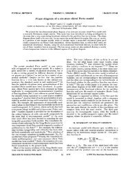
Fig. 1. AFM pictures <strong>of</strong> QDCs grown on a groove<br />
pattern oriented along [011] (a), [01-1] (b), [010] (c),<br />
and [001] (d) directions.The color scale in (a)-(d) is 26<br />
nm.<br />
Fig. 2. PL spectra from [01-1]-oriented QDCs measured at<br />
10K with different excitation laser powers. The inset<br />
shows polarization anisotropy <strong>of</strong> the PL emission. The<br />
radial axis <strong>of</strong> the polar plot represents relative PL intensity<br />
ranging from 0.9 to 1.1<br />
[1] J. Tommila, A. Tukiainen, J. Viheriälä, A. Schramm, T. Hakkarainen, A. Aho, P. Stenberg, M. Dumitrescu and M. Guina,<br />
”Nanoimprint lithography patterned GaAs templates for site-controlled InAs quantum dots”, to be published in J. Cryst.<br />
Growth.<br />
_________________________<br />
* Contact: teemu.hakkarainen@tut.fi