Book of abstracts - Euro-MBE 2011 - CNRS
Book of abstracts - Euro-MBE 2011 - CNRS
Book of abstracts - Euro-MBE 2011 - CNRS

You also want an ePaper? Increase the reach of your titles
YUMPU automatically turns print PDFs into web optimized ePapers that Google loves.
16th<br />
<strong>Euro</strong>pean<br />
<strong>MBE</strong><br />
<strong>2011</strong><br />
<strong>Book</strong> <strong>of</strong> Abstracts<br />
Photo: Laurent SALINO / Alpe d’Huez Tourisme<br />
16 th <strong>Euro</strong>pean Molecular Beam Epitaxy Workshop<br />
March 20 th -23 rd , <strong>2011</strong>, Alpe d’Huez, France
16th <strong>Euro</strong>pean Molecular Beam Epitaxy Workshop<br />
<strong>Book</strong> <strong>of</strong><br />
Abtracts<br />
March 20 – 23, <strong>2011</strong><br />
Congress Center, Alpe d’Huez<br />
France
The <strong>Euro</strong>-<strong>MBE</strong> Workshop is held biennially and began 30 years ago<br />
in Germany (1st <strong>Euro</strong>pean Workshop on <strong>MBE</strong>, Stuttgart, April 1981). It<br />
stands as one <strong>of</strong> the most renowned and prestigious scientific meetings on<br />
<strong>MBE</strong>. The last three Workshops were held in Grindelwald, Switzerland<br />
(2005), Sierra Nevada, Spain (2007), Zakopane, Poland (2009) and were<br />
highly successful, both from the participation viewpoint and from the high<br />
quality scientific standards.<br />
Topics<br />
- III-V, II-VI Materials and Heterostructures<br />
- Wide Bandgap Materials (III-Nitrides, Oxides, SiC)<br />
- Si, SiGe and Related Materials<br />
- Ferromagnets and Spintronics<br />
- Novel Materials<br />
- Low Dimensional Structures (Nanowires, Quantum Dots, …)<br />
- Fundamentals <strong>of</strong> <strong>MBE</strong> Growth, in-situ Monitoring<br />
- Devices and <strong>MBE</strong> production issues
Organizing Committee<br />
Serge TATARENKO (Chairman), Régis ANDRE, Edith BELLET-AMALRIC,<br />
Bruno DAUDIN, Véronique FAUVEL, Yann GENUIST, and Eva MONROY<br />
Technical support: Yoann CURE, Marion DUCRUET, Jean DUSSAUD<br />
Affiliation: CEA-<strong>CNRS</strong>-UJF group "Nanophysique et Semiconducteurs"<br />
Institut Néel - <strong>CNRS</strong> and INAC-CEA Grenoble (France)<br />
Program Committee<br />
• M. BUGAJSKI, Institute <strong>of</strong> Electron Technology, Warsaw (Poland)<br />
• T. FOXON, Univ. <strong>of</strong> Nottingham (UK)<br />
• N. GRANDJEAN, Ecole Polytechnique Federale de Lausanne (Switzerland)<br />
• D. GRÜTZMACHER, Institut für Bio- und Nanosysteme, Jülich (Germany)<br />
• M. HOPKINSON, Univ. <strong>of</strong> Sheffield (UK)<br />
• S. IVANOV, I<strong>of</strong>fe Phys-Technical Institute, St Petersburg (Russia)<br />
• J. MASSIES, CRHEA-<strong>CNRS</strong>, Valbonne (France)<br />
• J. OSTEN, Leibniz University, Berlin (Germany)<br />
• M. PESSA, Tampere Univ. <strong>of</strong> Technology (Finland)<br />
• H. RIECHERT, Paul-Drude-Institut, Berlin (Germany)<br />
• C. SKIERBISZEWSKI, Unipress, Warsaw (Poland)<br />
• L. SORBA, Instituto Nanoscienze-CNR, Pisa (I) (Italy)<br />
• G. SPRINGHOLZ, Johannes Kepler Univ., Linz (Austria)<br />
• E. TOURNIE, Univ. Montpellier 2 (France)<br />
• S. WANG, Chalmers Univ. <strong>of</strong> Technology, Gothenburg (Sweden)<br />
• W. WEGSCHEIDER, ETH Zürich (Switzerland)<br />
Contact Address<br />
Véronique FAUVEL Tel: +33 476 88 10 89<br />
Secrétariat Dépt. Nano Fax: +33 476 88 11 91<br />
Institut Néel – <strong>CNRS</strong><br />
E-Mail : embe<strong>2011</strong>@grenoble.cnrs.fr<br />
25 rue des Martyrs, B.P. 166 http://embe<strong>2011</strong>.neel.cnrs.fr/<br />
38042 Grenoble, France
Invited speakers<br />
D. AS, Paderborn Univ. (Germany)<br />
Recent device applications <strong>of</strong> non-polar cubic group III-nitrides<br />
O. BIERWAGEN, Univ. California Santa Barbara (USA)<br />
<strong>MBE</strong> <strong>of</strong> semiconducting oxides<br />
A. BONANNI, Johannes Kepler Univ., Linz (Austria)<br />
Controlling and visualizing the distribution <strong>of</strong> transition metals in nitrides<br />
J.-M. CHAUVEAU, CRHEA-<strong>CNRS</strong> (France)<br />
Polar and nonpolar (Zn,Mg)O/ZnO heterostructures : the benefits <strong>of</strong><br />
homoepitaxy<br />
M. EIBELHUBER, Johannes Kepler Univ., Linz (Austria)<br />
<strong>MBE</strong> growth <strong>of</strong> IV-VI quantum dots<br />
F. FURTMAYR, Walter Schottky Institut, Munich (Germany)<br />
Optical and structural properties <strong>of</strong> III-Nitride nanowires and nanowire<br />
heterostructures<br />
F. GLAS, LPN-<strong>CNRS</strong> (France)<br />
Growth kinetics <strong>of</strong> III-V nanowires<br />
M. GUINA, Tampere Univ. <strong>of</strong> Technology (Finland)<br />
Recent advances in <strong>MBE</strong> <strong>of</strong> dilute-nitrides and related device applications<br />
V. NOVAK, Institute <strong>of</strong> Physics ASCR, Prague (Czech Rep.)<br />
<strong>MBE</strong> growth <strong>of</strong> LiMnAs<br />
J.-B. RODRIGUEZ, Univ. Montpellier 2 (France)<br />
Current developments in <strong>MBE</strong> growth <strong>of</strong> highly mismatched materials<br />
S. SANGUINETTI, Univ. degli Studi Milano-Bicocca (Italy)<br />
GaAs based nanostructures grown by droplet epitaxy<br />
T. WIETLER, Leibniz Univ. Hannover (Germany)<br />
Surfactant-modified epitaxy <strong>of</strong> germanium layers on silicon for high<br />
mobility channels
Sponsors<br />
http://www.home.agilent.com/<br />
http://www.omicron.de/<br />
http://www.azeliselectronics.com/<br />
http://www.riber.com/<br />
http://rta-instruments.com/<br />
http://www.dca.fi/<br />
http://eurotherm.com/<br />
http://www.staibinstruments.com/<br />
http://www.hidenanalytical.com/<br />
http://www.surface-tec.com/ /<br />
http://www.mbe-kompo.de/<br />
http://www.vbseurope.com/<br />
http://www.oerlikon.com/leyboldvacuum/<br />
http://www.veeco.com/<br />
http://www.vinci-technologies.com/<br />
http://www.rhonealpes.fr/<br />
http://www.fondation-nanosciences.fr/
List <strong>of</strong> Exhibitors present on site, sponsors and the booth # :<br />
http://www.oerlikon.com/leyboldvacuum/<br />
#22<br />
http://altec-equipment.com/<br />
#20<br />
http://www.mbe-kompo.de/<br />
#18<br />
http://www.laytec.de/<br />
#12<br />
http://www.veeco.com/<br />
#7<br />
http://www.mewasa.ch/<br />
#11<br />
http://www.vbseurope.com/<br />
#6<br />
http://www.axt.com/<br />
#2<br />
http://www.dca.fi/<br />
#19<br />
http://www.samtelgmbh.com/<br />
#10<br />
http://www.riber.com/<br />
#14, #15<br />
http://www.mcse.fr/<br />
#4<br />
http://www.omicron.de/<br />
#17<br />
http://www.inficon.com/<br />
#5<br />
http://rta-instruments.com/<br />
#13<br />
http://www.wafertech.co.uk<br />
#21<br />
http://eurotherm.com/<br />
#8<br />
http://www.createc.de<br />
#1<br />
http://www.staibinstruments.com/<br />
#16<br />
http://www.wepcontrol.com/<br />
#3<br />
http://www.cvtechnology.com<br />
#4<br />
http://www.vinci-technologies.com/<br />
#9
Main locations<br />
for <strong>Euro</strong>-<strong>MBE</strong> <strong>2011</strong><br />
A : Hotel les Grandes Rousses<br />
B : Pierre & vacances<br />
C : Hotel Pic Blanc<br />
: (33) 4 76 11 42 42<br />
D : Palais des Congrés<br />
A<br />
D<br />
B<br />
C
Conference Program
Program <strong>of</strong> the 16th <strong>Euro</strong>pean Molecular Beam Epitaxy Workshop<br />
March 20 th -23 rd , <strong>2011</strong>, Alpe d’Huez<br />
Sunday, March 20 th<br />
11:00 – 20:00 Registration Lobby <strong>of</strong> Hotel Pic Blanc<br />
18:00 – 19:15 Welcome glass <strong>of</strong> wine<br />
Hotel Pic Blanc<br />
19:30 – 21:30 VEECO USERS’ MEETING<br />
Hotel Pic Blanc<br />
Time<br />
Monday, March 21 st<br />
8:15-8:30 OPENING SESSION<br />
GaAs based nanostructures grown by droplet epitaxy<br />
Monday<br />
8:30-9:00<br />
Mo1.1<br />
(invited)<br />
S.Sanguinetti, C. Somaschini, S. Bietti and N. Koguchi<br />
L-NESS and Dip. di Scienza dei Materiali, Università di Milano Bicocca, Italy<br />
Monday<br />
9:00-9:15<br />
Mo1.2<br />
Interfacial strains in InAs/AlSb multilayers for short<br />
wavelength quantum cascade lasers<br />
C. Gatel, B. Warot-Fonrose, A. Ponchet, C. Magen, R. Ibarra, R.<br />
Teissier and A.N. Baranov<br />
CEMES-<strong>CNRS</strong>, Toulouse, France<br />
Monday<br />
9:15-9:30<br />
Mo1.3<br />
Monday<br />
9:30-9:45<br />
Mo1.4<br />
Monday<br />
9:45-10:00<br />
Mo1.5<br />
Arsenides I<br />
200 mm GaAs wafers by <strong>MBE</strong> on SGOI and Ge/Si substrates<br />
M. Richter, T. Topuria, C. Marchiori, M. El-Kazzi, C. Rossel, C. Gerl,<br />
D.J. Webb, T. Smets, C. Andersson, M.Sousa, D. Caimi, L.<br />
Czornomaz, H. Siegwart, J.-F. Damlencourt, J.-M. Hartmann, P.M.<br />
Rice, and J. Fompeyrine<br />
IBM Research – Zurich, Switzerland<br />
Tuning the size, strain and band <strong>of</strong>fsets <strong>of</strong> InAs/GaAs<br />
quantum dots through a thin GaAs(Sb)(N) capping layer<br />
J.M. Ulloa, M. Montes, K. Yamamoto, A. Guzman, A. Hierro, M.<br />
Bozkurt, P.M. Koenraad, D. Fernández, D. González and D. Sales<br />
ISOM and Dpto. Ing. Electronica, Univ. Politecnica Madrid, 28040 Spain<br />
InAs Quantum Dot Chains Grown on Nanoimprint Lithography<br />
Patterned GaAs(100)<br />
T. V. Hakkarainen, A. Schramm, J. Tommila, A. Tukiainen, R.<br />
Ahorinta, M. Dumitrescu, M. Guina.<br />
Optoelectronics Research Centre, Tampere University <strong>of</strong> Technology,Finland<br />
10:00-10:30 COFFEE BREAK
<strong>MBE</strong> growth <strong>of</strong> LiMnAs<br />
Monday<br />
10:30-11:00<br />
Mo2.1<br />
(invited)<br />
V. Novak<br />
Institute <strong>of</strong> Physics ASCR, Prague, Czech Rep.<br />
Monday<br />
11:00-11:15<br />
Mo2.2<br />
Monday<br />
11:15-11:30<br />
Mo2.3<br />
Monday<br />
11:30-11:45<br />
Mo2.4<br />
Monday<br />
11:45-12:00<br />
Mo2.5<br />
Monday<br />
12:00-12:15<br />
Mo2.6<br />
Antimonides and Phosphides<br />
Growth and structural properties <strong>of</strong> InSb-based<br />
heterostructures<br />
A.N. Semenov, B.Ya. Meltser, V.A. Solov'ev, T.A. Komissarova,<br />
Ya.V. Teren't'ev, A.A. Sitnikova, and S.V. Ivanov<br />
I<strong>of</strong>fe Physical-Technical Institute <strong>of</strong> RAS, St. Petersburg , Russia<br />
Comparison <strong>of</strong> interface properties in two-dimensional<br />
heterostructures grown layer-by-layer or by step flow<br />
E. Luna , R. Hey, A. Guzmán and A. Trampert<br />
Paul-Drude Institut für Festkörperelektronik , Berlin, Germany<br />
<strong>MBE</strong> growth <strong>of</strong> (GaAsPN/GaPN)/GaP quantum wells light<br />
emitting diode<br />
A. Bondi, C. Cornet, W. Guo, O. Dehaese, N. Chevalier, C. Robert,<br />
T. Nguyen Thanh, S.Richard, M. Perrin, A. Létoublon, J. P. Burin. J.<br />
Even, O. Durand and A. Le Corre<br />
Université <strong>Euro</strong>péenne de Bretagne, INSA, FOTON, RENNES, France<br />
Lattice mismatch accommodation at the GaSb/GaAs and<br />
GaSb/GaP interfaces<br />
L. Desplanque, S. El Kazzi , C. Coinon, Y. Wang, P. Ruterana and X.<br />
Wallart<br />
IEMN, <strong>CNRS</strong> and University <strong>of</strong> Lille , France<br />
Defects in <strong>MBE</strong> grown InAs/GaSb superlattices<br />
on GaSb substrates<br />
M. Walther, R. Rehm1, J. Schmitz, J. Niemasz, F. Rutz, A. Wörl, L.<br />
Kirste, R. Scheibner, J. Ziegler, and A. Danilewsky<br />
Fraunh<strong>of</strong>er-Institut für Angewandte Festkörperphysik Freiburg, Germany<br />
BREAK 12:15 – 17:00<br />
Lunch at Hotel Pic Blanc or in a mountain restaurant <strong>of</strong> the resort + Free time
Making nitrides magnetic<br />
Monday<br />
17:00-17:30<br />
Mo3.1<br />
(invited)<br />
A. Bonanni<br />
Institut für Halbleiter- und Festkörperphysik, Johannes Kepler University,<br />
Linz - Austria<br />
Monday<br />
17:30-18:00<br />
Mo3.2<br />
(invited)<br />
Optical and structural properties <strong>of</strong> III-Nitride nanowires and<br />
nanowire heterostructures<br />
F. Furtmayr<br />
Walter Schottky Institut, Munich , Germany<br />
Monday<br />
18:00-18:15<br />
Mo3.3<br />
Monday<br />
18:15-18:30<br />
Mo3.4<br />
Monday<br />
18:30-18:45<br />
Mo3.5<br />
Monday<br />
18:45-19:00<br />
Mo3.6<br />
Nitrides<br />
Specialized <strong>MBE</strong> system for growth <strong>of</strong> high quality III-N<br />
heterostructures<br />
A. Alexeev , D. Krasovitsky, S.Petrov and V. Chaly<br />
SemiTEq JSC, St.Petersburg , Russia<br />
Improved luminescence and thermal stability <strong>of</strong> <strong>MBE</strong>-grown<br />
semipolar (11-22) InGaN quantum dots<br />
A.Das, Y. Kotsar, A. Lotsari, Th. Kehagias, Ph. Komninou, and E.<br />
Monroy<br />
CEA-<strong>CNRS</strong> group « Nanophysique et Semiconducteurs », Institut<br />
Néel/<strong>CNRS</strong>-Univ. J. Fourier and CEA, INAC, SP2M, Grenoble, France<br />
Group III-nitrides growth on N-polar substrates<br />
C. Cheze, M. Sawicka, M. Siekacz, H. Turski, G. Cywiński, B.<br />
Grzywacz, S. Grzanka, I. Dzięcielewski, B. Łucznik,<br />
M. Boćkowski, C. Skierbiszewski<br />
TopGaN Ltd, Warszawa, Poland<br />
<strong>MBE</strong> growth <strong>of</strong> GaN using in-situ SiN treatments<br />
F. Semond, E. Frayssinet, M. Leroux, Y. Cordier, M. Réda Ramdani,<br />
J.C. Moreno, S. Sergent, B. Damilano, P. Vennéguès, O. Tottereau<br />
and J. Massies<br />
CRHEA/<strong>CNRS</strong>, Sophia Antipolis, Valbonne, France<br />
POSTER SESSION MoP1<br />
19:00 – 20:45<br />
Cocktail buffet: regional specialties in the exhibition room<br />
21:00<br />
RIBER USERS’ MEETING
Program <strong>of</strong> the 16th <strong>Euro</strong>pean Molecular Beam Epitaxy Workshop<br />
March 20 th -23 rd , <strong>2011</strong>, Alpe d’Huez<br />
Time<br />
Tuesday, March 22 nd<br />
Advances <strong>of</strong> dilute-nitrides <strong>MBE</strong> technology and related<br />
device applications<br />
Tuesday<br />
8:30-9:00<br />
Tu1.1<br />
(invited)<br />
M. Guina, V.-M. Korpijärvi, J. Puustinen, A. Aho, T. Leinonen, and A.<br />
Tukiainen<br />
Tampere Univ. <strong>of</strong> Technology , Finland<br />
Tuesday<br />
9:00-9:15<br />
Tu1.2<br />
Current-injection lasing in GaAs quantum dots grown by<br />
droplet epitaxy<br />
M. Jo, T. Mano and K. Sakoda<br />
National Institute for Materials Science, Tsukuba, Japan<br />
Tuesday<br />
9:15-9:30<br />
Tu1.3<br />
Tuesday<br />
9:30-9:45<br />
Tu1.4<br />
Tuesday<br />
9:45-10:00<br />
Tu1.5<br />
Arsenides II<br />
<strong>MBE</strong> growth <strong>of</strong> high power Modelocked Integrated External-<br />
Cavity Surface Emitting Laser (MIXSEL) with 6.4 W output<br />
power<br />
M. Golling, B. Rudin, V. J. Wittwer, D. J. H. C. Maas, Y. Barbarin, M.<br />
H<strong>of</strong>fmann, O. D. Sieber, T. Südmeyer, U. Keller<br />
Department <strong>of</strong> Physics, Ultrafast Laser Physics Lab, ETH Zurich, Switzerland<br />
1.55 μm lasers based on shape-engineered<br />
InAs/InAlGaAs/InP (100) quantum dots<br />
C. Gilfert, V. Ivanov and J.P. Reithmaier<br />
Technische Physik, Institute <strong>of</strong> Nanostructure Technologies and Analytics,<br />
University <strong>of</strong> Kassel, Germany<br />
Broadband emission and mode-locking using controlled<br />
distributions <strong>of</strong> InGaAs quantum dots<br />
M. Hopkinson, M. Hugues , P.D.L. Greenwood , M.Krakowski, M.<br />
Calligaro, S.Bruer, , M. Rossetti, W. Elsäßer, I. Montrosset<br />
Department <strong>of</strong> Electronic and Electrical Engineering, University <strong>of</strong> Sheffield,<br />
UK<br />
10:00-10:30 COFFEE BREAK
Tuesday<br />
10:30-11:00<br />
Tu2.1<br />
(invited)<br />
Current developments in <strong>MBE</strong> growth <strong>of</strong> highly mismatched<br />
materials<br />
J.-B. Rodriguez<br />
Univ., Montpellier 2, France<br />
<strong>MBE</strong> <strong>of</strong> semiconducting oxides<br />
Tuesday<br />
11:00-11:30<br />
Tu2.2<br />
(invited)<br />
O. BIERWAGEN<br />
Univ. California Santa Barbara , USA<br />
Tuesday<br />
11:30-11:45<br />
Tu2.3<br />
Tuesday<br />
11:45-12:00<br />
Tu2.4<br />
Tuesday<br />
12:00-12:15<br />
Tu2.5<br />
New trends in <strong>MBE</strong><br />
<strong>MBE</strong> growth <strong>of</strong> the topological insulator Bi2Te3 on Si (111)<br />
Substrates<br />
G. Mussler, J. Krumrain , L. Plucinski , and D. Grützmacher<br />
Institute <strong>of</strong> Bio- and Nanosystems 1, Research Center Jülich, Germany<br />
Atomic-scale mapping <strong>of</strong> quantum dots using direct x-ray<br />
methods<br />
R. Clarke, D.P. Kumah ,+, R.S. Goldman , V. Dasika , C. Schlepütz ,<br />
Y. Yacoby, E. Cohen , and Y. Paltiel<br />
University <strong>of</strong> Michigan, Department <strong>of</strong> Physics, Ann Arbor, USA<br />
II-VI-based microcavities for the blue-violet spectral range<br />
S. Klembt, C. Kruse , M. Seyfried , K. Sebald , J. Gutowski and D.<br />
Hommel<br />
Institute <strong>of</strong> Solid State Physics, Semiconductor Epitaxy, University <strong>of</strong><br />
Bremen, Germany<br />
BREAK 12:15 – 17:00<br />
Lunch at Hotel Pic Blanc or in a mountain restaurant <strong>of</strong> the resort + Free time
Tuesday<br />
17:00-17:30<br />
Tu3.1<br />
(invited)<br />
Recent device applications <strong>of</strong> non-polar cubic group IIInitrides<br />
D. As<br />
Paderborn Univ., Germany<br />
Tuesday<br />
17:30-18:00<br />
Tu3.2<br />
(invited)<br />
Polar and nonpolar (Zn,Mg)O/ZnO heterostructures : the<br />
benefits <strong>of</strong> homoepitaxy<br />
J.-M. Chauveau<br />
CRHEA-<strong>CNRS</strong>, Sophia Antipolis, France<br />
Tuesday<br />
18:00-18:15<br />
Tu3.3<br />
Tuesday<br />
18:15-18:30<br />
Tu3.4<br />
Tuesday<br />
18:30-18:45<br />
Tu3.5<br />
Tuesday<br />
18:45-19:00<br />
Tu3.6<br />
Wide bandgap<br />
A bi-layer oxide buffer approach for the integration <strong>of</strong> single<br />
crystalline GaN on Si (111) platform<br />
L. Tarnawska, P. Zaumseil, M. Kittler, P. Storck, R. Paszkiewicz,<br />
and T. Schroeder<br />
IHP, Im Technologiepark 25, Frankfurt (Oder), Germany<br />
GaN/AlGaN superlattices grown by PA<strong>MBE</strong> for intersubband<br />
applications in the infrared spectral range<br />
Y. Kotsar, A. Das, E. Bellet-Amalric, E. Sarigiannidou, H.<br />
Machhadani, S. Sakr, M. Tchernycheva, F. H. Julien and E. Monroy<br />
CEA-<strong>CNRS</strong> group « Nanophysique et Semiconducteurs », Institut<br />
Néel/<strong>CNRS</strong>-Univ. J. Fourier and CEA, INAC, SP2M, Grenoble, France<br />
Growth and Characterization <strong>of</strong> ZnO/ZnMgO Quantum Wells<br />
B. Laumer, Fabian Schuster, Thomas Wassner, Martin Stutzmann,<br />
and Martin Eickh<strong>of</strong>f<br />
Walter Schottky Institut, Technische Universität München, Garching,<br />
Germany<br />
InGaN laser diodes operating at 450-455 nm grown by RF-<br />
Plasma <strong>MBE</strong><br />
M Siekacz, H. Turski, M. Sawicka, G. Cywiński, J. Smalc-<br />
Koziorowska, P. Wiśniewski, P. Perlin, I. Grzegory and C.<br />
Skierbiszewski<br />
Institute <strong>of</strong> High Pressure Physics, Polish Academy <strong>of</strong> Sciences, Warszawa,<br />
Poland<br />
POSTER SESSION TuP2<br />
19:00 – 20:45<br />
Cocktail buffet:regional specialties in the exhibition room<br />
21:00<br />
WORKSHOP BANQUET
Program <strong>of</strong> the 16th <strong>Euro</strong>pean Molecular Beam Epitaxy Workshop<br />
March 20 th -23 rd , <strong>2011</strong>, Alpe d’Huez<br />
Time<br />
Wednesday, March 23 rd<br />
Surfactant-modified epitaxy <strong>of</strong> germanium layers on silicon<br />
for high mobility channels<br />
Wednesday<br />
9:00-9:30<br />
We1.1<br />
(invited)<br />
T. Wietler<br />
Leibniz Univ. Hannover , Germany<br />
Wednesday<br />
9:30-9:45<br />
We1.2<br />
Wednesday<br />
9:45-10:00<br />
We1.3<br />
Wednesday<br />
10:00-10:15<br />
We1.4<br />
Group IV materials<br />
Epitaxial growth <strong>of</strong> SrTiO3 on Si : strain relaxation and<br />
formation <strong>of</strong> tetragonal domains<br />
G. Saint-Girons, G. Niu, J. Penuelas, L. Largeau, B. Vilquin, J.L.<br />
Maurice C. Botella and G. Hollinger<br />
Université de Lyon, Institut des Nanotechnologies de Lyon, Ecole Centrale<br />
de Lyon, France<br />
Morphology and luminescence properties <strong>of</strong> Sb mediated<br />
Ge/Si quantum dots<br />
A.A. Tonkikh, N.D. Zakharov, V.G. Talalaev, A.V. Novikov, K.<br />
Kudryavtsev,B. Fuhrmann, H.S. Leipner, P. Werner<br />
Max-Planck Institute <strong>of</strong> Microstructure Physics, Halle, Germany<br />
Growth <strong>of</strong> small-period Si/Ge quantum dot crystals by <strong>MBE</strong><br />
S. Borisova, C. Dais ,J.C. Gerharz , G. Mussler and D. Grützmacher<br />
Institute <strong>of</strong> Bio- and Nanosystems 1, Forschungszentrum Jülich, Germany<br />
Wednesday<br />
10:15-10:30<br />
We1.5<br />
In situ STM and RHEED study <strong>of</strong> tensile strained Si grown on<br />
Ge (001) substrates<br />
B. Sanduijav, D. Matei, and G. Springholz<br />
Institut für Halbleiter- und Festkörperphysik, Johannes Kepler University,<br />
Linz, Austria<br />
10:30-11:00 COFFEE BREAK
Wednesday<br />
11:00-11:30<br />
We2.1<br />
(invited)<br />
<strong>MBE</strong> growth <strong>of</strong> IV-VI quantum dots for MIR devices<br />
M. Eibelhuber, A. Hochreiner, T. Schwarzl, H. Groiss, W. Heiss1, G.<br />
Springholz ,V. Kolkovsky, G. Karczewski, and T. Wojtowicz<br />
Johannes Kepler Univ., Linz , Austria<br />
Wednesday<br />
11:30-11:45<br />
We2.2<br />
Wednesday<br />
11:45-12:00<br />
We2.3<br />
Wednesday<br />
12:00-12:15<br />
We2.4<br />
Wednesday<br />
12:15-12:30<br />
We2.5<br />
Wednesday<br />
12:30-12:45<br />
We2.6<br />
Devices<br />
The role <strong>of</strong> doping scheme in ultra-low disorder <strong>MBE</strong> grown<br />
mesoscopic FQHE devices<br />
V. Umansky , M. Heiblum, M. Dolev and Y. Gross<br />
Braun Center for Submicron Research, Weizmann Institute <strong>of</strong> Science,<br />
Israel<br />
Investigations <strong>of</strong> Si-dopant layers on ultrahigh-mobility 2<br />
DEGs in GaAs/AlGaAs-structures<br />
C. Reichl, E. de Wiljes, C. Rössler and W. Wegscheider<br />
ETH Zürich, Laboratorium für Festkörperphysik, 8093 Zürich, Switzerland<br />
Short wavelength high power Quantum Cascade Lasers<br />
X. Marcadet, M. Carras, B. Simozrag, M. Garcia,<br />
G. M. De Naurois, G. Maisons, O. Parillaud, O. Patard, F.<br />
Pommereau, O. Drisse, F. Alexandre, J. Massies<br />
Alcatel Thales III-V Lab, 91767 Palaiseau cedex, France<br />
<strong>MBE</strong> growth <strong>of</strong> InGaAs/GaAsSb based mid-infrared and THz<br />
quantum cascade lasers<br />
H. Detz, A.M. Andrews , P. Klang , C. Deutsch , M. Nobile , W.<br />
Schrenk , K. Unterrainer and G. Strasser<br />
Center for Micro- and Nanostructures and Institute for Solid-State<br />
Electronics, Vienna University <strong>of</strong> Technology, 1040 Wien, Austria<br />
Room temperature operation <strong>of</strong> a GaInAsSb/AlGaInAsSb<br />
digital alloy laser diode at 3.3 μm<br />
S. Belahsene, K. S.Gadedjisso1, G. Boissier1, P. Grech1, G. Narcy<br />
and Y. Rouillard<br />
Institut d'Electronique du Sud, UMR 5214 <strong>CNRS</strong>, Université Montpellier 2,<br />
Montpellier, France<br />
BREAK 12:45–14:45<br />
Lunch at Hotel Pic Blanc
Growth kinetics <strong>of</strong> III-V nanowires<br />
Wednesday<br />
14:45-15:15<br />
We3.1<br />
(invited)<br />
F. Glas<br />
LPN-<strong>CNRS</strong>, Marcoussis, France<br />
Wednesday<br />
15:15-15:30<br />
We3.2<br />
Wednesday<br />
15:30-15:45<br />
We3.3<br />
Wednesday<br />
15:45-16:00<br />
We3.4<br />
Wednesday<br />
16:00-16:15<br />
We3.5<br />
Wednesday<br />
16:15-16:30<br />
We3.6<br />
Nanowires<br />
InAs Quantum Dot Arrays Decorating the Facets <strong>of</strong> GaAs<br />
Nanowires<br />
E. Uccelli, J. Arbiol , J.R. Morante , A. Fontcuberta i Morral<br />
Laboratoire des Matériaux Semiconducteurs, Ecole Polytechnique Fédérale<br />
de Lausanne, Switzerland<br />
AlAs-GaAs core-shell nanowires grown by chemical beam<br />
epitaxy<br />
A. Li, D. Ercolani , F. Rossi , L. Nasi , G. Salviati, F. Beltram and L.<br />
Sorba<br />
NEST, Istituto Nanoscienze-CNR and Scuola Normale Superiore, Pisa, Italy<br />
Distinct nucleation and growth modes <strong>of</strong> self-assisted InAs<br />
nanowires on bare Si(111)<br />
E. Dimakis, J. Lähnemann, U. Jahn, S. Breuer, M. Hilse, L.<br />
Geelhaar, and H. Riechert<br />
Paul Drude Institute for Solid State Electronics, Berlin, Germany<br />
Strain balanced technique for the growth <strong>of</strong> very high aspect<br />
ratio quantum posts<br />
D. Alonso-Álvarez, B. Alén, J. M. Ripalda, J. Llorens, A. G.<br />
Taboada, Y. González, L. González, F. Briones, M. A. Roldán, J.<br />
Hernandez-Saz, M. Herrera and S.I. Molina<br />
IMM-Instituto de Microelectrónica de Madrid, Spain<br />
Polarity <strong>of</strong> GaN nanowires grown by Plasma-Assisted<br />
Molecular Beam Epitaxy<br />
K. Hestr<strong>of</strong>fer, C. Bougerol, C. Leclere, H. Renevier, J. L. Rouvière<br />
and B. Daudin<br />
CEA-<strong>CNRS</strong> group « Nanophysique et Semiconducteurs », Institut<br />
Néel/<strong>CNRS</strong>-Univ. J. Fourier and CEA, INAC,SP2M, Grenoble, France<br />
16:30-17:00<br />
Award ceremony - Closing address<br />
Free time<br />
Free access to keep-fit center, swimming pool, spa<br />
at Hotel Pic Blanc<br />
Starting 19:00<br />
Farewell Dinner
RHEED<br />
S T A I B INSTRUMENTS<br />
Powerful In-Situ Growth Characterization<br />
PEEM<br />
S T A I B INSTRUMENTS<br />
PhotoElectron Emission Microscope<br />
For <strong>MBE</strong>, PLD,<br />
Laser <strong>MBE</strong>, CVD<br />
etc.<br />
Growth control<br />
Oscillation detection<br />
Latice spacing<br />
UHV and high pressure<br />
Visit<br />
us<br />
at<br />
www.staibinstruments.com<br />
Electron Sources<br />
Nanotechnology<br />
Surface Analysis<br />
Scanning Imaging<br />
Space Simulation<br />
SUPER<br />
Cylindrical Mirror Analyzer<br />
Energy Analzyzer AES / XPS / UPS<br />
Thermal Processing<br />
Evaporation<br />
Ionization
Poster sessions<br />
Monday & Tuesday
POSTER SESSION 1<br />
Monday, March 21 st 19:00 – 20:45<br />
OPENING SESSION<br />
MoP01<br />
Post-heat treatment on the improvement <strong>of</strong> efficiency in<br />
CdTe thin film solar cells.<br />
Deliang Wang ,Zhizhong Bai.<br />
MoP02<br />
MoP03<br />
MoP04<br />
MoP05<br />
Sn doped GaAs by CBE using tetramethyltin.<br />
C. García Núñez, D. Ghita, B. J. García.<br />
Early stages <strong>of</strong> the growth <strong>of</strong> InP and GaAs islands on<br />
SrTiO3 substrates.<br />
B. Gobaut, J. Penuelas, A. Chettaoui, J. Cheng, G. Grenet,<br />
L. Largeau and G. Saint-Girons.<br />
Growth directions and structural properties <strong>of</strong> InP<br />
nanowires fabricated on Si and SrTiO3 substrates.<br />
J. Penuelas, K. Naji, H. Dumont, G. Saint-Girons, G. Patriarche,<br />
M. Gendry.<br />
Optimization <strong>of</strong> <strong>MBE</strong>-grown AlSb/InAs High Electron<br />
Mobility Transistor Structures.<br />
H. Zhao , G. Moschetti , S. Wang , P-Å. Nilsson , and J. Grahn.<br />
MoP06<br />
MoP07<br />
MoP8<br />
Monolithic integration <strong>of</strong> InP based heterostructures on<br />
silicon using SrTiO3 templates.<br />
A. Chettaoui, B. Gobaut, J. Penuelas, J. Cheng1, G. Niu, L.<br />
Largeau, P. Regreny, G. Saint-Girons.<br />
Crystal structure X-ray investigation <strong>of</strong> InAs nanorods on<br />
Si(111).<br />
A. Davydok , A. Biermanns , M. Dimakis, S. Breuer, L. Geelhaar,<br />
and U. Pietsch.<br />
Structural and optical properties <strong>of</strong> InN films grown on<br />
ZnO(000-1) by plasma-assisted molecular beam epitaxy.<br />
Y. J. Cho, O. Brandt, M. Ramsteiner, M. Wienold and H. Riechert.<br />
MoP09<br />
Multifunctional Epitaxial Nanocomposite Films by L<strong>MBE</strong>.<br />
J.Xiong.
POSTER SESSION 1<br />
Monday, March 21 st 19:00 – 20:45<br />
OPENING SESSION<br />
MoP10<br />
MoP11<br />
MoP12<br />
MoP13<br />
MoP14<br />
Near infrared high efficiency InAs/GaAsSb QDLEDs: band<br />
alignment and carrier recombination mechanisms.<br />
A. Hierro, M. Montes, M. Moral, J.M. Ulloa, A. Guzman.<br />
In-situ Reflectance Anisotropy Spectroscopy (RAS) for<br />
doping control during <strong>MBE</strong> growth <strong>of</strong> AlGaInAsSb laser<br />
structures .<br />
D. H<strong>of</strong>fmann , T. Loeber and H. Fouckhardt.<br />
Effect <strong>of</strong> growth temperature on surface morphology <strong>of</strong><br />
selectively grown GaN layers by ammonia-based metalorganic<br />
molecular beam.<br />
S. Naritsuka , C. H. Lin, R. Abe, S. Uchiyama, Y. Uete<br />
and T. Maruyama .<br />
Investigation <strong>of</strong> the local electronic structure <strong>of</strong> Cu-doped<br />
GaN grown by plasma assisted <strong>MBE</strong>.<br />
R. Schuber, P.R. Ganz , F. Wilhelm , A. Rogalev ,<br />
and D.M. Schaadt.<br />
Growth Optimization for InAs/GaSb T2SL Structures by<br />
<strong>MBE</strong>.<br />
Y. X. Song , S. M. Wang, C. Asplund, H. Malm, X. Lu, J. Shao.<br />
MoP15<br />
MoP16<br />
A prototype <strong>of</strong> heterovalent interfaces: Reduction <strong>of</strong> the<br />
potential barrier in the conduction band at the n-ZnSe /<br />
n-GaAs in.<br />
A. Frey, U. Bass, S. Mahapatra, C. Schumacher, J. Geurts<br />
and K. Brunner.<br />
Effect <strong>of</strong> growth temperature on quantum dot laser (Ga,In)<br />
(N,As) self-assembled quantum dots.<br />
O. A. Niasse, M. AL Khalfioui, B. Ba, A. Bèye, M. Leroux.<br />
MoP17<br />
MoP18<br />
Effect <strong>of</strong> different monolayer coverage for the seed layer in<br />
quaternary alloy capped multilayer InAs/GaAs quantum<br />
dot system.<br />
S. Chakrabarti ,A. Mandal and N. Halder .<br />
Neutron reflectometry studies <strong>of</strong> hetero-interfacial H layer<br />
in highly lattice-mismatched epitaxy on Si.<br />
H. Asaoka, T. Yamazaki, D. Yamazaki, M. Takeda<br />
and S. Shamoto.
POSTER SESSION 1<br />
Monday, March 21 st 19:00 – 20:45<br />
OPENING SESSION<br />
MoP19<br />
MoP20<br />
Surface Electronic Properties <strong>of</strong> GaAs Nanowires.<br />
O. Demichel, M. Heiss, J. Bleuse , H. Mariette, A. Fontcuberta.<br />
Critical thickness <strong>of</strong> 2D-3D and “hut”-“dome” transitions<br />
at the growth <strong>of</strong> GexSi1-x and Ge/GexSi1-x layers on the<br />
Si(100).<br />
V.A. Tim<strong>of</strong>eev , A.I. Nikiforov , V.V. Ulyanov , O.P. Pchelyakov.<br />
MoP21<br />
Epitaxy and characterization <strong>of</strong> GaMnAs.<br />
Martin Utz , D. Schuh , D. Bougeard and W. Wegscheider.<br />
MoP22<br />
MoP23<br />
MoP24<br />
MoP25<br />
MoP26<br />
MoP27<br />
Mid-infrared Quantum Dot LEDs and microdisk laser grown<br />
by <strong>MBE</strong><br />
A. Hochreiner, M. Eibelhuber, T. Schwarzl, H. Groiss, V.<br />
Kolkovsky, G. Karczewski, T. Wojtowicz, W. Heiss, G. Springholz.<br />
High-quality structures <strong>of</strong> InAs QDs in Al0.9Ga0.1As<br />
matrix grown by droplet epitaxy.<br />
A.A.Lyamkina, D.S. Abramkin, D.V.Dmitriev, S.P.Moshchenko,<br />
. T.S. Shamirzaev, A. I. Toropov,K. S. Zhuravlev.<br />
Structural properties <strong>of</strong> InAlN single layers nearly latticematched<br />
to GaN grown by plasma assisted molecular beam<br />
epitaxy.<br />
Ž. Gacevic1, S. Fernández-Garrido and E. Calleja, D. Hosseini,<br />
S. Estradé and F. Peiró.<br />
Composition studies <strong>of</strong> site-controlled quantum dots.<br />
G. Biasiol, V. Baranwal , S. Heun, M. Prasciolu, M. Tormen,<br />
A. Locatelli, T. O. Mentes, M. N. Orti, and L. Sorba.<br />
Single InAs quantum dots morphology and local electronic<br />
properties on (113)B InP substrate.<br />
C. Cornet , P. Turban , N. Bertru , S. Tricot , O. Dehaese<br />
and A. Le Corre.<br />
Investigations <strong>of</strong> growth kinetics <strong>of</strong> InN using pulsed RF<br />
<strong>MBE</strong>.<br />
A. Kraus , R. E. Buß, H. Bremers, U. Rossow, and A. Hangleiter.
POSTER SESSION 1<br />
MoP28<br />
MoP29<br />
MoP30<br />
MoP31<br />
MoP32<br />
MoP33<br />
MoP34<br />
MoP35<br />
MoP36<br />
Monday, March 21 st 19:00 – 20:45<br />
OPENING SESSION<br />
Low Thermal Budget Fabrication <strong>of</strong> Local Artificial<br />
Substrates by Droplet Epitaxy on Silicon.<br />
S.Bietti, C.Somaschini, N.Koguchi and S.Sanguinetti.<br />
Investigation <strong>of</strong> improvement and degradation <strong>of</strong> thermal<br />
annealed indium rich InGaN/GaN quantum wells grown by<br />
NH3-<strong>MBE</strong>.<br />
N. A. K. Kaufmann, A. Dussaigne , D. Martin and N. Grandjean .<br />
Shape Changes in Patterned Planar InAs as a Function <strong>of</strong><br />
Thickness and Temperature.<br />
K.G. Eyink , L. Grazulis , K. Mahalingham , M. Twyman , J. Shoaf,<br />
V. Hart , J. Hoelscher , C. Claflin, and D. Tomich.<br />
Influence <strong>of</strong> Al on the group III-assisted growth <strong>of</strong> axial<br />
AlGaAs/GaAs heterostructure nanowires.<br />
T. Rieger , M. I. Lepsa , H. Lüth , T. Schäpers<br />
and D. Grützmacher.<br />
Ferromagnetic and transport properties <strong>of</strong> very thin<br />
(Ga,Mn)As layers.<br />
L. Ebel, F. Greullet, T. Naydenova, J. Constantino, S. Mark,<br />
C. Gould, K. Brunner and L.W. Molenkamp.<br />
Self-assembled InP-nanoneedles grown on (001) InP by<br />
gas source <strong>MBE</strong>.<br />
M. Chashnikova, V. Bryksa, A. Mogilatenko, O. Fedosenko, S.<br />
Machulik, M.P.Semtsiv, W. Neumann, and W.T. Masselink.<br />
Selective growth <strong>of</strong> InP on pre-patterned wafers by the<br />
means <strong>of</strong> Gas-Source <strong>MBE</strong>.<br />
A.Aleksandrova, G.Monastyrskyi, O.Fedosenko, M.Chashnikova ,<br />
S.Machulik ,J.Kishkat , M.P.Semtsiv and T.W.Masselink.<br />
Scaling <strong>of</strong> quantum cascade laser efficiency with a number<br />
<strong>of</strong> cascades.<br />
O.Fedosenko, A.Aleksandrova , G.Monastyrskyi, M.Chashnikova ,<br />
S.Machulik ,J.Kishkat, M.Klinkmüller, M.P.Semtsiv,T.W.Masselink.<br />
<strong>MBE</strong> growth <strong>of</strong> quantum-cascade laser on pre-patterned<br />
substrates.<br />
G. Monastyrskyi, O. Fedosenko, M. Chashnikova, A. Alexandrova,<br />
. S. Machulik,J.Kischkat, M. Klinkmüller, M. P. Semtsiv<br />
and W. T. Masselink.
POSTER SESSION 1<br />
MoP37<br />
Monday, March 21 th -- 19:00 – 20:45<br />
OPENING SESSION<br />
Non polar GaN/ZnO heterostructures grown by ammonia<br />
source molecular beam epitaxy.<br />
J. Brault, G. Sophia, S. El Kazzi, J.-M. Chauveau, P. Vennéguès,<br />
M. Nemoz, M. Teisseire, M. Leroux, C. Deparis, C. Morhain,<br />
O. Tottereau, L. Nguyen.<br />
MoP38<br />
MoP39<br />
Emission <strong>of</strong> colloidal nano-crystals embedded in <strong>MBE</strong><br />
grown ZnSe microstructures.<br />
J. Kampmeier, M. Rashad , A. Pawlis, D. Schikora, K. Lischka.<br />
Reproducible temperature calibration technique for GaAs<br />
<strong>MBE</strong>.<br />
François Morier-Genoud and Denis Martin.
POSTER SESSION 2<br />
Tuesday, March 22 nd 19:00 – 20:45<br />
TuP01<br />
TuP02<br />
OPENING SESSION<br />
Fabrication and optical properties <strong>of</strong> CdTe quantum dots in<br />
ZnTe nanowires.<br />
P. Wojnar, E. Janik , A. Petroutchik , L. Baczewski , M. Goryca ,<br />
T. Kazimierczuk , P. Kossacki , G. Karczewski and T. Wojtowicz.<br />
In-situ, real time Auger Monitoring as a new tool for<br />
growth characterization and control.<br />
P. Staib.<br />
TuP03<br />
Optimisation <strong>of</strong> Unusual Quantum Dot Growth Conditions<br />
for Optical Coherence Tomography Applications.<br />
M. Hugues , M. A. Majid , S. Vezian , D. T. D. Childs , K. Kennedy<br />
. and R. A.Hogg.<br />
TuP04<br />
A New Route for Strain relaxation in In0.52Al0.48As on<br />
GaAs Grown by <strong>MBE</strong>.<br />
S. M. Wang ,Y. X. Song , Z. H. Lai, M. Sadeghi and J. R. Dong.<br />
TuP05<br />
Nonpolar III-nitride microcavities for polariton lasing.<br />
A. Dussaigne, G. Rossbach, J. Levrat, H. Teisseyre, I. Grzegory,<br />
R. Butté, TSuski, and N. Grandjean.<br />
Annealing effects on site-selective InAs quantum dots.<br />
TuP06<br />
TuP07<br />
M. Helfrich , J. Hendrickson , M. Gehl , D. Rülke , D. Z. Hu, M.<br />
Hetterich ,S. Linden , M. Wegener , H. Kalt , G. Khitrova ,<br />
H. M. Gibbs and D. M. Schaadt.<br />
Comparison <strong>of</strong> InAs quantum dots grown by ripening on<br />
InP and GaInAsP buffer layers on InP(001).<br />
P. Regreny, A. Benamrouche, C. Brillard and M. Gendry.<br />
TuP08<br />
TuP09<br />
Study on homoepitaxial germanium nanowire growth.<br />
J. Schmidtbauer, R. Bansen, T. Boeck, R. Heimburger,<br />
Th. Teubner and T. Schoeder.<br />
Correlating electronic and structural properties <strong>of</strong> Gaassisted<br />
GaAs nanowires via cathodoluminescence<br />
imaging.<br />
J. Kasprzak,J.-S. Hwang, F. Donatini, C. Bougerol, H. Mariette,<br />
Le Si Dang and R. Songmuang.
POSTER SESSION 2<br />
Tuesday, March 22 nd 19:00 – 20:45<br />
OPENING SESSION<br />
Growth and microstructure <strong>of</strong> GaN:Cu.<br />
TuP10<br />
TuP11<br />
TuP12<br />
P. R. Ganz , G. Fischer , C. Sürgers, H. T. Hsing , L. Chang<br />
And D. M. Schaadt.<br />
Different strategies towards the deterministic coupling <strong>of</strong><br />
a Single QD to a Photonic Crystal Cavity Mode.<br />
J.Herranz, I.Prieto, Y.González, J.Canet‐Ferrer, P.A.Postigo,<br />
B.Alén, L.González, L.J.Martínez, M.Kaldirim, D. Fuster,<br />
G.Muñoz‐Matutano, and J.Martínez‐Pastor.<br />
Capping effect on the morphological and optical properties<br />
<strong>of</strong> GaAs/AlGaAs quantum structures.<br />
M. Jo, G. Duan, T. Mano and K. Sakoda.<br />
TuP13<br />
Optical signatures <strong>of</strong> dopant complexes in Arsenic doped<br />
HgCdTe epilayers.<br />
F. Gemain , I. C. Robin , B. Polge and A. Lusson.<br />
TuP14<br />
TuP15<br />
Optical properties <strong>of</strong> post-growth annealed type-II GaSb<br />
quantum dots.<br />
A. Schramm, V. Polojärvi, T. V. Hakkarainen, A. Gubanov,<br />
J. Paajaste, R.Koskinen, S. Suomalainen, and M. Guina.<br />
Metamorphic 6.3Å GaInSb templates grown on GaAs<br />
substrates for mid-infrared lasers.<br />
L.Cerutti , J.B. Rodriguez and E. Tournié.<br />
TuP16<br />
Reflection high-energy electron diffraction phi scans forthe<br />
in-situ monitoring <strong>of</strong> the growth <strong>of</strong> GaN nanowires on Si.<br />
P. Dogan , O. Brandt, L. Geelhaar, and H. Riechert.<br />
TuP17<br />
TuP18<br />
Optical polarization from self-organized InP QDs grown on<br />
an self-undulated template.<br />
A. Ugur, F. Hatami, N. Vamivakas L.Lombez ,M. Atatüre<br />
B. and W. T. Masselink.<br />
The <strong>MBE</strong> growth <strong>of</strong> HgCdTe on CdZnTe and CdTe/Ge at<br />
CEA-LETI.<br />
Giacomo Badano, Philippe Ballet, Sebastien Renet,<br />
Philippe Duvaut, Xavier Baudry,Bernard Polge and Alain Million.
POSTER SESSION 2<br />
Tuesday, March 22 nd 19:00 – 20:45<br />
TuP19<br />
OPENING SESSION<br />
Control <strong>of</strong> nitrogen plasma for growth <strong>of</strong> GaN by plasmaassisted<br />
<strong>MBE</strong>.<br />
Z.R. Zytkiewicz, M. Sobanska, K. Klosek, H. Teisseyre, A.<br />
Wierzbicka, E. Lusakowska, and W. Jung.<br />
GaN/AlN semipolar quantum dots for ultra-violet emission.<br />
TuP20<br />
TuP21<br />
A. Kahouli , N. Kriouche , J. Brault , B. Damilano , P. de Mierry ,<br />
. A. Courville , J.Massies.<br />
<strong>MBE</strong> growth approaches for improving Sb-based<br />
In0.5Ga0.5As(Sb)/GaAs QDs.<br />
M.J. Milla , Á. Guzmán, J.M. Ulloa, A. Hierro.<br />
TuP22<br />
Post-growth rapid thermal annealing <strong>of</strong> InAs quantum<br />
dots grown on GaAs nanoholes formed by droplet epitaxy.<br />
B. Alén, L. Wewior, D. Fuster, L. Ginés, Y. González, J. M.<br />
Llorens, D. Alonso-Álvarez, and L. González.<br />
TuP23<br />
Ga blocking effect for GaN growth with NH3.<br />
B. Damilano , A. Kahouli , J. Brault , D. Lefebvre , and J. Massies.<br />
TuP24<br />
Use <strong>of</strong> RHEED to optimize atomic layering <strong>of</strong> complex<br />
Oxides.<br />
B. A. Davidson, A. Yu. Petrov and S. Nannarone.<br />
TuP25<br />
TuP26<br />
TuP27<br />
II-VI nanostructures, with type-II band alignment, for<br />
photovoltaics.<br />
R. André, E. Bellet-Amalric, J. Bleuse, C. Bougerol,<br />
M. Den Hertog, L. Gérard, H. Mariette.<br />
Enhanced intermixing in Ge nano-prisms on groove<br />
patterned Si (1 1 10) substrates.<br />
G. Chen, G. Vastola, J. J. Zhang, B. Sanduijav, G. Springholz,<br />
W. Jantsch, F. Schäffler.<br />
Influence <strong>of</strong> nitrogen flux on InGaN growth by PA<strong>MBE</strong>.<br />
H. Turski , M Siekacz , M. Sawicka , G. Cywiński , M. Kryśko ,<br />
S. Grzanka ,I. Grzegory , S. Porowski , Z. Wasilewski<br />
and C. Skierbiszewski.
POSTER SESSION 2<br />
TuP28<br />
TuP29<br />
TuP30<br />
Tuesday, March 22 nd 19:00 – 20:45<br />
OPENING SESSION<br />
Growth <strong>of</strong> metal Co/Ag superlattices on MgO(001):<br />
microstructure and magnetic characterization.<br />
Ana Ruiz, Enrique Navarro, María Alonso, Pilar Ferrer,<br />
Daniel Margineda, F. Javier Palomares, Federico Cebollada,<br />
Jesús Mª González.<br />
Quantum dot formation from sub-critical InAs layers<br />
grown on metamorphic InGaAs .<br />
P. Frigeri , G. Trevisi and L. Seravalli.<br />
Reversible Nan<strong>of</strong>acetting and 1D Ripple Formation <strong>of</strong> Ge<br />
on High-Indexed Si (11 10) Substrat.<br />
G. Springholz, B. Sanduijav and D. Matei.<br />
TuP31<br />
TuP32<br />
TuP33<br />
TuP34<br />
TuP35<br />
Homoepitaxy and nitrogen doping<br />
<strong>of</strong> non polar ZnO films.<br />
D. Tain<strong>of</strong>f, J.-M. Chauveau, C. Deparis, B. Vinter, M. AlKhalfioui,<br />
M. Teisseire, Christian Morhain.<br />
Structural characterization <strong>of</strong> <strong>MBE</strong> grown GaP/Si<br />
nanolayers.<br />
A. Létoublon, W. Guo, G. Elias, C. Cornet, A. Ponchet, A. Bondi,<br />
T. Rohel, N.Bertru, C. Robert, T. Nguyen Thanh, O. Durand,<br />
J.S. Micha and A. Le Corre.<br />
An Auger Electron Analyzer System for In situ <strong>MBE</strong><br />
Stoichiometry Control.<br />
W. Laws Calley, Phillipe Staib, Jonathan Lowder,<br />
and W. Alan Doolittle.<br />
<strong>MBE</strong> droplet epitaxy <strong>of</strong> InGaAs/Ga (100): effect <strong>of</strong> <strong>MBE</strong><br />
conditions and post-annealings on (Ga,In)droplet and<br />
GaInAs nanostructure morphology and emission.<br />
Chantal Fontaine, Poonyasiri Boonpeng, Guy Lacoste, Alexandre<br />
Arnoult, Hejer Makhloufi, Olivier Gauthier-Lafaye, Guilhem<br />
Almuneau, Somchai Ratanathammaphan, Somsak Panyakeow.<br />
Synthesis <strong>of</strong> AlGaN nanowires by Molecular Beam Epitaxy.<br />
A. Pierret , C. Bougerol , B. Gayral , B. Attal-Trétout ,<br />
A. Loiseau and B.Daudin .<br />
TuP36<br />
Correlation <strong>of</strong> structural, chemical and optical characterization<br />
<strong>of</strong> CdSe quantum dots inserted in ZnSe nanowires<br />
M. Elouneg-Jamroz, M. den Hertog, S. Bounouar, E. Bellet-<br />
Amalric, R. André,Y. Genuist, K. Kheng, J-P Poizat, S. Tatarenko.
POSTER SESSION 2<br />
Tuesday, March 22 nd 19:00 – 20:45<br />
OPENING SESSION<br />
Optical and structural properties <strong>of</strong> InGaN/GaN nanowires.<br />
TuP37<br />
G. Tourbot , C. Bougerol, C. Leclere, B. Gayral, P. Gilet,<br />
H. Renevier and B. Daudin.<br />
TuP38<br />
Position controlled self-catalyzed growth <strong>of</strong> GaAs<br />
nanowires by molecular beam epitaxy.<br />
Andreas Rudolph, Joachim Hubmann, Markus Kargl,<br />
Benedikt Bauer, Marcello Soda, Josef Zweck, Dieter Schuh,<br />
Dominique Bougeard and Elisabeth Reiger.
TERRITORY<br />
Silicon Wafers, Ultrapure Silicon Dopant <strong>MBE</strong><br />
GaAs wafers FREIBERGER<br />
EUROPE except Germany,Austria<br />
InP wafers INPACT EUROPEAN research centers<br />
GaSb,GaP,,InAs,InSb<br />
SIMS and RBS Analysis Service PROBION<br />
ARSENIC 7N,7N5 <strong>MBE</strong> slugs, FURUKAWA<br />
GALLIUM 7N+, 7N5 +( RRR > 75000) <strong>MBE</strong><br />
ALUMINIUM 6N5 , the purest in the world<br />
INDIUM 7N <strong>MBE</strong><br />
PHOSPHOROUS 7N <strong>MBE</strong>,6 N RASA<br />
BERYLLIUM 5N+ <strong>MBE</strong><br />
EUROPE<br />
WORLD except France,Japan<br />
EUROPE<br />
EUROPE<br />
WORLD<br />
EUROPE<br />
EUROPE<br />
WORLD<br />
Bi, Cd, Pb, Sb, Sn, Te, Zn, Se, Th, Mg6N, Mn 5N8, S 6 or 6N +GaTe,GeS pieces<br />
PBN, PG crucibles,pieces<br />
WORLD<br />
WORLD<br />
Ga Recycling, GaAs, InP Wafers Reclaim<br />
Bonding Wires and Ribbons MEM.SUMITOMO METAL MINING<br />
Bonding Caps-Wedges, Pick up tools , Die Collets, SPT ROTH<br />
Western/Eastern EUROPE<br />
FRANCE<br />
Resinoid Blades THERMOCARBON<br />
www.azeliselectronics.com<br />
Tel : 0033-1-44 73 10 70 Fax : 0033-1-44 73 10 53 – Azelis.Electronics@Azelis.fr
Monday Session Mo1<br />
Arsenides I
Mo1.1<br />
GaAs based nanostructures grown by droplet epitaxy<br />
S.Sanguinetti * , C. Somaschini § , S. Bietti and N. Koguchi<br />
L-NESS and Dip. di Scienza dei Materiali, Università di Milano Bicocca, Via Cozzi 53, 20125 Milano, Italy<br />
What makes three dimensional semiconductor quantum nanostructures (QN) so attractive is the<br />
possibility to tune their electronic properties by careful design <strong>of</strong> their size and composition. These<br />
parameters set the confinement potential <strong>of</strong> electrons and holes, thus determining the electronic and<br />
optical properties <strong>of</strong> the QN. An <strong>of</strong>ten overlooked parameter, which has a even more relevant effect on<br />
the electronic properties <strong>of</strong> the QN, is shape. Gaining a strong control over the electronic properties <strong>of</strong><br />
semiconductor nanostructure via shape tuning is the key to access electronic fine design possibilities.<br />
We present an innovative growth method, the Dropled Epitaxy (DE) [1,2], a variant <strong>of</strong> molecular<br />
beam epitaxy, for the fabrication <strong>of</strong> semiconductor III-V QNs with highly designable shapes and<br />
complex morphologies. In short, the DE growth procedure consists <strong>of</strong> first irradiating the substrate<br />
with a group III molecular beam flux, leading to the formation <strong>of</strong> numerous, nanometer-sized, metallic<br />
droplets on the surface which are subsequently crystallized into nanostructures by a group V molecular<br />
beam. With DE is possible to combine multiple single QNs, namely quantum dots, quantum rings<br />
and quantum disks, with tunable sizes and densities, into a single multi-functional QN thus allowing<br />
an unprecedented control over the electronic properties <strong>of</strong> the QNs [2,3] (see Figure 1). In addition,<br />
DE is intrinsically a low thermal budget growth <strong>of</strong> III-V materials, being fully performed at 200-<br />
350°C. This makes DE perfectly suited for the realization <strong>of</strong> growth procedures compatible with backend<br />
integration <strong>of</strong> III-V materials on Si [4,5].<br />
Fig 1: Three examples <strong>of</strong> possible complex quantum strcutures fabricated by Droplet Epitaxy: (left panel) double<br />
concentric double rings, (central panel) triple concentric quantum rings and (right panel) coupled ring disks.<br />
[1] N. Koguchi, et al., J. Cryst. Growth (1991), 111, 688<br />
[2] C. Somaschini, et al., Nano Letters 2009, 9, 3419<br />
[3] C. Somaschini, et al., Nanotechnology 2010, 21, 125601<br />
[4] S. Bietti, et al., Appl. Phys. Lett. 2009, 95, 241102<br />
[5] C. Somaschini, et al. Appl. Phys. Lett. 2010, 97, 053101<br />
* Corresponding author: stefano.sanguinetti@unimib.it<br />
§ Present Address: Paul Drude Institut, Berlin (D)
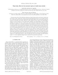
Mo1.2<br />
Interfacial strains in InAs/AlSb multilayers for short wavelength<br />
quantum cascade lasers<br />
C. Gatel 1,3 , B. Warot-Fonrose 1,3 , A. Ponchet 1,* , C.Magen 2,3 , R.Ibarra 2,3 , R. Teissier 4<br />
and A.N. Baranov 4<br />
1<br />
CEMES-<strong>CNRS</strong>, 29 rue Jeanne Marvig 31055 Toulouse, France<br />
2 INA, Universidad de Zaragoza, C/ Mariano Esquillor, Edificio I+D, 50018 Zaragoza, Spain<br />
3<br />
TALEM Associated Laboratory <strong>CNRS</strong>-University <strong>of</strong> Zaragoza, 29 rue Jeanne Marvig 31055 Toulouse, France<br />
4 IES-UMR 5214, <strong>CNRS</strong>-Université Montpellier 2, 34095 Montpellier, France<br />
This work explores the interfacial strain in InAs/AlSb multilayers grown by <strong>MBE</strong> on InAs(001)<br />
substrates. Due to the remarkably high discontinuity <strong>of</strong> the conduction band (2.1 eV), InAs/AlSb<br />
constitutes a highly interesting system for quantum cascade lasers (QCLs). These devices can cover<br />
the wavelength region from 2.7 to 4.0 µm, well beyond the limits <strong>of</strong> QCLs based on the well matured<br />
InP system [1,2].<br />
In InAs/AlSb based QCLs, the wavelength <strong>of</strong> emission mainly depends on the layers thicknesses,<br />
which have to be controlled at a fraction <strong>of</strong> monolayer. In addition, to allow the tunnel effect between<br />
adjacent InAs wells, the AlSb barriers can be locally as thin as 4 or 5 atomic planes. So, the interfacial<br />
zones cannot be neglected. The well and the barriers do not present common atoms: the interfaces<br />
consist <strong>of</strong> either AlAs or InSb bonds. Consequently, while the average lattice mismatch is low (1.3%),<br />
interfaces are susceptible to concentrate high lattice distortion. Indeed, in the bulk state AlAs and InSb<br />
presents lattice mismatch with InAs <strong>of</strong> -7% and 7%, respectively. Schematically, the interfaces can be<br />
tensile (Al-As type), compressive (In-Sb type) or neutral (alloyed type).<br />
We have grown different samples with various procedures which aim at tuning the interfacial zones. In<br />
a first sample, so-called reference sample, the procedure consisted in a simple growth interruption <strong>of</strong> 3<br />
seconds under As flux for the AlSb on InAs interfaces, under Sb flux for the InAs on AlSb interfaces.<br />
In other samples, we modified the growth sequences to intentionnaly favour either the Al-As or the In-<br />
Sb type interfaces, by modifying the group V flux and/or the duration <strong>of</strong> growth interruptions. The<br />
samples were examined by high resolution electron microscopy (HREM) on a TECNAI F-20 equipped<br />
with a corrector <strong>of</strong> spherical aberration, in order to analyse the out-<strong>of</strong>-plane strain pr<strong>of</strong>iles [3,4].<br />
Fig.1 (reference sample) shows a relatively symmetric pr<strong>of</strong>ile at the two interfaces. The negative out<strong>of</strong>-plane<br />
lattice distortion suggests a moderate tensile stress, probably due to the formation <strong>of</strong> Al-As<br />
type interfaces. It has been possible to modify qualitatively and quantitatively this pr<strong>of</strong>ile. An example<br />
is given in fig. 2, where a strong negative strain is achieved at the AlSb on InAs interface; this<br />
suggests the formation <strong>of</strong> a tensile interfacial zone <strong>of</strong> the Al-As type. A strong positive strain is<br />
achieved at the reverse interface; this suggests the formation <strong>of</strong> a compressive interfacial zone mainly<br />
<strong>of</strong> the In-Sb type. Chemical mapping using high angle annular dark field (HAADF) performed on a<br />
probe-corrected STEM (fig.3) evidences an asymmetry <strong>of</strong> the two interfaces in agreement with the<br />
hypothesis <strong>of</strong> an Al-As type interface for the AlSb on InAs interface.<br />
To summarize, interfacial strains in InAs/AlSb multilayers have been studied. High compressive and<br />
tensile stresses have been revealed at interfaces between InAs and AlSb in some samples. Specific<br />
<strong>MBE</strong> growth sequences were used to control composition and strain <strong>of</strong> interfacial zones.<br />
[1] J. Devenson, D. Barate, R. Teissier, and A. N. Baranov, Electronics Letters, 42, 1284-1286 (2006).<br />
[2] J. Devenson, O. Cathabard, R. Teissier, and A. N. Baranov, Applied Physics Letters, 91, 141106 (2007)<br />
[3] M.J. Hÿtch, E. Snoeck, and R. Kilaas, Ultramicroscopy 74, 131 (1998)<br />
[4] C. Gatel et al, Acta Mat., 58, 3238 (2010)<br />
[5] This research was supported by C’NANO GSO (<strong>CNRS</strong>, France)<br />
* Contact: anne.ponchet@cemes.fr
Mo1.2<br />
-3% +3%<br />
(a)<br />
(b)<br />
Fig 1: Reference sample (InAs and AlSb thicknesses are 20 nm and 4 nm, respectively).<br />
(a) HREM image in zone axis, (b) map <strong>of</strong> variation <strong>of</strong> the out-<strong>of</strong>-plane lattice parameter (the reference is<br />
InAs), and pr<strong>of</strong>ile <strong>of</strong> this variation across the small window.<br />
-6% +6%<br />
(a)<br />
(b)<br />
Fig 2: Same than fig.1 in a modified sample where Al-As and In-Sb interfaces have been favored by the growth<br />
sequences adopted at interfaces.<br />
(a)<br />
(b)<br />
Fig 3: STEM HAADF image <strong>of</strong> the same sample than in fig.2 (a) general view, (b) detail.<br />
The AlSb on InAs interface is characterized by a darker contrast than InAs and AlSb. This is the signature <strong>of</strong> a light<br />
material compared with InAs and AlSb, in agreement with the hypothesis <strong>of</strong> an Al-As type interface.
Mo1.3<br />
200 mm GaAs wafers by <strong>MBE</strong> on SGOI and Ge/Si substrates<br />
M. Richter 1,* , T. Topuria 2 , C. Marchiori 1 , M. El-Kazzi 1 , C. Rossel 1 , C. Gerl 1 , D.J. Webb 1 ,<br />
T. Smets 3 , C. Andersson 1 , M. Sousa 1 , D. Caimi 1 , L. Czornomaz 1 , H. Siegwart 1 ,<br />
J.-F. Damlencourt 4 , J.-M. Hartmann 4 , P.M. Rice 2 , and J. Fompeyrine 1<br />
1<br />
IBM Research – Zurich, Säumerstrasse 4, 8803 Rüschlikon, Switzerland<br />
2 IBM Research – Almaden, 650 Harry Road, San Jose, California, USA<br />
3 Kath. Uni. Leuven – Celestijnenlaan 200D, 3001 Heverlee, Belgium<br />
4 CEA-LETI – Grenoble, 17 rue des Martyrs, 38054 Grenoble, France<br />
The use <strong>of</strong> production size wafers is a prerequisite for the integration <strong>of</strong> III-V materials in future<br />
CMOS technology. Besides obvious technical benefits to merge III-V with silicon process technology,<br />
it also allows to economize on scarce materials. In this presentation, GaAs heterogeneous integration<br />
on 200 mm Si and SGOI wafers via Ge buffers will be discussed.<br />
In our previous work, we have studied thin (≤ 250 nm) <strong>MBE</strong>-grown Ge buffers. This had the<br />
advantage to rely on the use <strong>of</strong> two UHV-connected <strong>MBE</strong> chambers, thus limiting air exposure<br />
between Ge buffer and GaAs growth [1]. In this paper, we discuss an alternative approach which<br />
consists in combining Ge growth by reduced pressure-chemical vapor deposition (RP-CVD) with<br />
subsequent, ex-situ <strong>MBE</strong> GaAs deposition. CVD growth allows for thicker Ge layers and anneals in<br />
the H 2 carrier gas. By this means reduced defect densities [2] and flatter surfaces due to the surfactant<br />
action <strong>of</strong> H 2 [3] can be achieved. In a first series <strong>of</strong> samples, we use 200 mm Si(001) wafers with 1.5<br />
µm Ge. In a second series <strong>of</strong> sample, we use 200 mm SGOI wafers, which feature improved insulation<br />
to the Si substrate and optional co-integration <strong>of</strong> fully depleted GOI p-FETs [4].<br />
Special care needs to be taken to clean the Ge/Si or SGOI wafers before the GaAs <strong>MBE</strong> growth. The<br />
anneal temperature should be minimized to take account <strong>of</strong> the limited temperature stability. All<br />
wafers were prepared with an HF-dip as last cleaning step. Then, they were either exposed to a remote<br />
hydrogen plasma [5] or annealed at 600 °C in UHV. The removal <strong>of</strong> oxides and carbon was monitored<br />
with x-ray photoelectron spectroscopy (XPS). The H plasma efficiently removes oxide species at<br />
temperatures as low as 250 °C on both Ge/Si and SGOI substrates (spectra in Fig. 1). Only traces <strong>of</strong> C<br />
contamination are observed after such cleaning treatment. As opposed to that, after sample flash<br />
substantial amounts <strong>of</strong> SiOx are observed (Fig. 1(b)).<br />
For the SGOI wafers, either 200 nm Ge were deposited in a UHV-connected Si/Ge <strong>MBE</strong> system or<br />
SGOI wafers capped with 20 nm CVD-grown Ge were used. Then, the wafers were directly<br />
transferred under UHV conditions for epitaxy <strong>of</strong> 500 nm GaAs. Fig. 2 shows corresponding reflection<br />
high energetic electron diffraction (RHEED) images after the individual steps.<br />
We will discuss the impact <strong>of</strong> the substrate, its cleaning and <strong>of</strong> the different buffers on the GaAs<br />
structural quality. Cross-sectional transmission electron microscopy (XTEM) and atomic force<br />
microscope (AFM) images <strong>of</strong> a first sample <strong>of</strong> 500 nm GaAs on 20 nm Ge CVD-capped SGOI are<br />
shown in Fig. 3 (a) and (b), respectively.<br />
TEM specimen preparation by L.M. Clark and L.E. Krupp (IBM Research - Almaden) as well as<br />
financial support by the <strong>Euro</strong>pean Commission in frame <strong>of</strong> the FP7 project DUALLOGIC is gratefully<br />
acknowledged.<br />
[1] M. Richter, C. Rossel, D.J. Webb, T. Topuria, C. Gerl, M. Sousa, C. Marchiori, D. Caimi, H. Siegwart, P.M. Rice and J.<br />
Fompeyrine, “GaAs on 200 mm Si wafers via thin temperature graded Ge buffers by molecular beam epitaxy” submitted to J.<br />
Cryst. Growth and abstract <strong>MBE</strong> 2010 conference.<br />
[2] J.M. Hartmann, A. Abbadie, N. Cherkashin, H. Grampeix, and L. Clavelier, Semicond. Sci. Technol., 24, 055002 (2009).<br />
[3] L. Colace, G. Masini, F. Galluzzi, G. Assanto, G. Capellini, L. Di Gaspare, E. Palange, and F. Evangelisti, Appl. Phys.<br />
Lett., 72, 3175 (1998).<br />
[4] W. Van Den Daele, E. Augendre, K. Romanjek, C. Le Royer, L. Clavelier, J.-F. Damlencourt, E. Guiot, B. Ghyselen, and<br />
S. Cristoloveanu, ECS Trans., 19, 145 (2009).<br />
[5] C. Marchiori, D. J. Webb, C. Rossel, M. Richter, M. Sousa, C. Gerl, R. Germann, C. Andersson, and J. Fompeyrine, J.<br />
Appl. Phys., 106, 114112 (2009).<br />
__________________________<br />
* Contact: mri@zurich.ibm.com
Mo1.3<br />
(a)<br />
(b)<br />
Fig 1: XPS after the different cleaning steps <strong>of</strong> (a) Ge/Si and (b)SGOI wafers.<br />
(a)<br />
(c)<br />
(b)<br />
Fig 2: RHEED image <strong>of</strong> 200 mm Ge/Si wafer, (a) as loaded, (b) after Hydrogen clean, (c) after 500 nm GaAs growth.<br />
(a)<br />
(b)<br />
Fig 3: 500 nm GaAs on 20 nm CVD-grown Ge on SGOI, (a) XTEM image, (b) AFM image.
Mo1.4<br />
Tuning the size, strain and band <strong>of</strong>fsets <strong>of</strong> InAs/GaAs quantum<br />
dots through a thin GaAs(Sb)(N) capping layer<br />
J.M. Ulloa 1,* , M. Montes 1 , K. Yamamoto 1 , A. Guzman 1 , A. Hierro 1 , M. Bozkurt 2 ,<br />
P.M. Koenraad 2 , D. Fernández 3 , D. González 3 and D. Sales 3<br />
1 ISOM and Dpto. Ing. Electronica, Univ. Politecnica Madrid, Ciudad Universitaria s/n, 28040 Spain<br />
2 COBRA-PSN, Eindhoven University <strong>of</strong> Technology, P.O. Box 513, NL-5600MB Eindhoven, The Netherlands<br />
3 Departamento de Ciencia de los Materiales e I. M. y Q. I., Facultad de Ciencias, Universidad de Cádiz, Spain<br />
A common approach used in the past few years to extend the emission wavelength <strong>of</strong> InAs/GaAs<br />
quantum dots (QD) to the 1.3-1.55 µm range is the use <strong>of</strong> a strain reducing layer. By using thin<br />
GaAsSb capping layers, photoluminescence (PL) emission at 1.55 µm has been demonstrated [1-3].<br />
Nevertheless, adding Sb to the capping layer does not only affect the QD strain, but also the<br />
QD/capping layer valence band <strong>of</strong>fset, giving rise to a type-II band alignment at high Sb contents (~<br />
17 %). The result is that emission at long wavelengths can only be achieved in these structures with a<br />
type-II band alignment that degrades the PL. On the other hand, introducing small amounts <strong>of</strong> N in the<br />
capping layer would strongly reduce the QD/capping layer conduction band <strong>of</strong>fset, inducing an extra<br />
red shift. This could allow reaching 1.55 µm while keeping a type-I band alignment. In this work, we<br />
show how the height, strain and QD/capping layer band <strong>of</strong>fsets can be tuned by using a thin<br />
GaAs(Sb)(N) capping layer, allowing to reach emission in the 1.55 µm region. A detailed analysis<br />
by means <strong>of</strong> PL, cross-sectional scanning tunneling microscopy, transmission electron<br />
microscopy and atomic force microscopy allows correlating the optical and structural<br />
properties <strong>of</strong> the QD structures.<br />
The analyzed samples were grown by solid source <strong>MBE</strong> on n+ Si doped (100) GaAs<br />
substrates. In all <strong>of</strong> the samples 2.7 monolayers (ML) <strong>of</strong> InAs were deposited at 450 °C and<br />
0.035 ML/s on an intrinsic GaAs buffer layer. The QDs were capped with a nominally 5 nm<br />
thick GaAs(Sb)(N) layer grown at 470 °C. The nominal Sb and N contents were changed<br />
from 0 to 30 % and 0 to 3 %, respectively.<br />
Besides the expected reduction in the QD strain and the transition to a type-II band alignment<br />
at high Sb contents, we find that the QD height can be controlled through the amount <strong>of</strong> Sb in<br />
the capping layer due to reduced In-Ga intermixing during the capping process [4]. Figure 1<br />
shows how the QD height increases progressively with the amount <strong>of</strong> Sb, reaching the value<br />
<strong>of</strong> uncapped QDs for ~ 13% Sb. The increased height leads to improved PL at moderate Sb<br />
contents compared to the reference GaAs-capping sample (Fig. 2). On the other hand, GaAsN<br />
capping layers strongly reduce the QD conduction band <strong>of</strong>fset inducing also a PL red shift but<br />
preserving the type-I alignment and the optical quality (see Fig. 2). The impact <strong>of</strong> N on the<br />
structural properties <strong>of</strong> the QDs will be discussed. The longest wavelengths are achieved with<br />
the simultaneous presence <strong>of</strong> both Sb and N in the capping layer (Fig. 3), which allows to<br />
independently modify the conduction and valence band <strong>of</strong>fsets. Nevertheless, in this case the<br />
PL spectra are degraded compared to the case <strong>of</strong> the counterpart ternary alloys (Fig. 2).<br />
Although a type-I band alignment is preserved in this case even at the longest wavelengths,<br />
increasing the N content in the GaAsSb capping layer induces a progressive degradation <strong>of</strong><br />
the PL spectrum (Fig. 3). The reasons for this are investigated and will be discussed.<br />
[1] K. Akahane et al., Physica E (Amsterdam) 21, 295 (2004).<br />
[2] J. M. Ripalda et al., Appl. Phys. Lett. 87, 202108 (2005).<br />
[3] H. Y. Liu et al., J. Appl. Phys. 99, 046104 (2006).<br />
[4] J.M. Ulloa et al., Phys.Rev.B. 81,165305 (2010).<br />
_____________<br />
* Contact: jmulloa@die.upm.es
Mo1.4<br />
Capped QD height/Uncapped QD height<br />
1.1<br />
1.0<br />
0.9<br />
0.8<br />
0.7<br />
0.6<br />
0.5<br />
0.4<br />
0.3<br />
GaAsSb<br />
Reduced<br />
decomposition<br />
Completely<br />
supressed<br />
decomposition<br />
0 3 6 9 12 15 18 21 24<br />
Sb content (%)<br />
Fig 1: QD height normalized to the height <strong>of</strong> the uncapped<br />
QDs as a function <strong>of</strong> the Sb content. A value <strong>of</strong> 1.0<br />
indicates a completely suppressed decomposition process.<br />
The two different background colors indicate two different<br />
regimes regarding QD decomposition.<br />
250<br />
200<br />
GaAsSb<br />
(~13%)<br />
15 K<br />
PL intensity (a.u.)<br />
150<br />
100<br />
50<br />
GaAs<br />
GaAsN<br />
GaAsSbN<br />
x 10<br />
0<br />
1000 1100 1200 1300 1400<br />
Wavelength (nm)<br />
Fig 2: 15 K PL spectra <strong>of</strong> InAs/GaAs QDs grown under<br />
the same conditions and capped with different alloys.<br />
1,2<br />
GaAsSbN<br />
> N<br />
15 K<br />
Normalized PL intensity<br />
1,0<br />
0,8<br />
0,6<br />
0,4<br />
0,2<br />
0 % N<br />
0,0<br />
1000 1100 1200 1300 1400 1500 1600<br />
Wavelength (nm)<br />
Fig 3: Normalized 15 K PL spectra <strong>of</strong> a series <strong>of</strong> samples<br />
with constant Sb and increasing N content in the capping<br />
layer.
Mo1.5<br />
InAs Quantum Dot Chains Grown on Nanoimprint Lithography<br />
Patterned GaAs(100)<br />
T. V. Hakkarainen*, A. Schramm, J. Tommila, A. Tukiainen, R. Ahorinta, M.<br />
Dumitrescu, M. Guina.<br />
Optoelectronics Research Centre, Tampere University <strong>of</strong> Technology,<br />
P.O. Box 692, FIN-33101 Tampere, Finland.<br />
The ability to fabricate Stranski-Krastanov quantum dots on pre-determined locations, i.e. sitecontrolled<br />
growth, is essential for enabling emerging nanophotonic applications, such as photonic<br />
integrated circuits incorporating quantum dot chains (QDCs) as nanophotonic waveguides. As a<br />
method for the fabrication <strong>of</strong> site-controlled InAs QDCs, we combine growth by molecular beam<br />
epitaxy and nanoimprint lithography (NIL) [1]. NIL is able to produce sub 10 nm linewidths with high<br />
throughput and enables fast processing <strong>of</strong> large wafer area.<br />
In this paper we focus on studying structural and optical properties <strong>of</strong> QDCs with varying orientations<br />
with respect to the substrate crystal directions. The investigated samples were prepared in three stages.<br />
In the first stage, a 100 nm GaAs buffer, a 100 nm AlGaAs layer, and a 100 nm GaAs were deposited<br />
at 590 °C on n-GaAs(100) substrates by <strong>MBE</strong>. Then grooves were ex situ patterned by UV-NIL. The<br />
groove width was 90 nm, depth 30 nm, and period 180 nm. In the final stage, the patterned surface<br />
was covered with a 60 nm GaAs regrowth buffer at 490 °C and 2.2 ML InAs QDs grown at 515 °C.<br />
For optical investigation, the QDs were covered with GaAs and AlGaAs layers. We show that this<br />
method enables the simultaneous growth <strong>of</strong> QDCs oriented along [011], [01-1], [010], and [001]<br />
directions (Fig. 1) exhibiting strong photoluminescence (PL) emission at room temperature. Being<br />
able to form QDCs with different orientations with at the same growth conditions is crucial for the<br />
fabrication <strong>of</strong> QDC networks for integrated circuits. Furthermore, we report low temperature PL<br />
(temperature, power, and polarization dependencies) for the optical characterization <strong>of</strong> the QDCs and<br />
atomic force microscopy (AFM) based facet analysis for investigating the morphology <strong>of</strong> the patterned<br />
surface.<br />
(a)<br />
(c)<br />
[011]<br />
(b)<br />
(d)<br />
[01-1]<br />
PL intensity (arb. units)<br />
1.0<br />
0.8<br />
0.6<br />
0.4<br />
0.2<br />
0.0<br />
[0-11]<br />
[011]<br />
[0-1-1]<br />
[01-1]<br />
4.5 mW<br />
1.2 mW<br />
0.7 mW<br />
0.1 mW<br />
1.1 1.2 1.3 1.4<br />
Energy (nm)<br />
Fig. 1. AFM pictures <strong>of</strong> QDCs grown on a groove<br />
pattern oriented along [011] (a), [01-1] (b), [010] (c),<br />
and [001] (d) directions.The color scale in (a)-(d) is 26<br />
nm.<br />
Fig. 2. PL spectra from [01-1]-oriented QDCs measured at<br />
10K with different excitation laser powers. The inset<br />
shows polarization anisotropy <strong>of</strong> the PL emission. The<br />
radial axis <strong>of</strong> the polar plot represents relative PL intensity<br />
ranging from 0.9 to 1.1<br />
[1] J. Tommila, A. Tukiainen, J. Viheriälä, A. Schramm, T. Hakkarainen, A. Aho, P. Stenberg, M. Dumitrescu and M. Guina,<br />
”Nanoimprint lithography patterned GaAs templates for site-controlled InAs quantum dots”, to be published in J. Cryst.<br />
Growth.<br />
_________________________<br />
* Contact: teemu.hakkarainen@tut.fi
Monday Session Mo2<br />
Antimonides & Phosphides
Mo2.1<br />
<strong>MBE</strong> growth <strong>of</strong> LiMnAs<br />
Vít Novák<br />
Institute <strong>of</strong> Physics <strong>of</strong> the Academy <strong>of</strong> Sciences, Cukrovarnická 10, 162 53 Praha, Czech Republic<br />
Compound semiconductors derived from silicon have had a tremendous impact on the physics and<br />
applications <strong>of</strong> semiconductors. Two textbook examples are the direct gap III-V semiconductors and<br />
the prototype magnetic II-VI semiconductors, Fig.1. Remarkably, none <strong>of</strong> the other closest relatives <strong>of</strong><br />
silicon from the I-III-IV and I-II-V compounds have so far been synthesized by modern epitaxial<br />
growth techniques and the potential <strong>of</strong> these compounds has remained virtually unexplored. In this<br />
talk we focus on I-Mn-V compounds which surprisingly have not previously been considered as<br />
candidate semiconductors. One <strong>of</strong> the key motivations to establish their semiconducting electronic<br />
structure is that they are among the rare known silicon relatives with magnetic ordering temperature<br />
safely above room temperature.<br />
Fig.1: Closest relatives <strong>of</strong> silicon emerging by applying the “proton transfer” rule.<br />
We demonstrate on LiMnAs that high-quality materials with group-I alkali metals in the crystal structure<br />
can be grown by standard solid source molecular beam epitaxy [1]. The epitaxial LiMnAs film exhibits<br />
optical gap, evidenced by optical transmission measurements and consistent with the band structure<br />
obtained by our ab initio calculations. Squid magnetometry measurements support earlier reports <strong>of</strong><br />
high antiferromagnetic ordering temperature.<br />
We propose a strategy for employing I-Mn-V compounds in high-temperature semiconductor<br />
magneto-electronics. The key principle is to utilize relativistic magnetic and magneto-transport anisotropy<br />
effects whose common characteristics is that they are an even function <strong>of</strong> the microscopic magnetic<br />
moment vector and are therefore in principle equally well present in materials with ferromagnetic (FM) and<br />
antiferromagnetic (AFM) order. The application <strong>of</strong> AFM semiconductors to exchange bias FMs opens an<br />
immediate research opportunity for integrating conventional semiconductor micro and opto-electronics<br />
functionalities directly in the exchange-biasing AFM layers in common magneto-electronic devices. In<br />
these structures LiMnAs can be combined, e.g., with lattice matched FM semiconductor (In,Mn)As or<br />
conventional transition metal FMs. The FM-AFM coupling can also be used for controlling the staggered<br />
moment orientation in the AFM by the exchange spring effect induced by rotating moments in the<br />
ferromagnet.<br />
[1] T. Jungwirth, et al., Phys. Rev. B 83, 035321 (<strong>2011</strong>).<br />
_______________________<br />
* Contact: vit.novak@fzu.cz
Mo2.2<br />
Growth and structural properties <strong>of</strong> InSb-based heterostructures<br />
A.N. Semenov, B.Ya. Meltser, V.A. Solov'ev, T.A. Komissarova, Ya.V. Teren't'ev,<br />
A.A. Sitnikova, and S.V. Ivanov<br />
I<strong>of</strong>fe Physical-Technical Institute <strong>of</strong> RAS, Polytekhnicheskaya 26, St. Petersburg 194021, Russia<br />
Among III-V semiconductors, indium antimonide has the narrowest band gap and the smallest<br />
effective electron mass that results in a record value <strong>of</strong> room-temperature electron mobility in bulk<br />
InSb layer as well as 2D electron gas (2DEG). This makes InSb a very attractive material for new<br />
generation <strong>of</strong> high speed devices like a high electron mobility transistor (HEMT) [1] and IR<br />
photodetectors [2]. Al x In 1-x Sb alloys can be used as barriers for the InSb QW heterostructures but Al<br />
content is limited by x~0.2 due to abrupt increase <strong>of</strong> the stress in high Al-content alloys grown on<br />
InSb. This paper reports on <strong>MBE</strong> growth, structural, optical, and transport properties <strong>of</strong> InSb,<br />
Al x In 1-x Sb (0≤x≤0.3) and their QW heterostructures.<br />
All the structures were grown on semi-insulated GaAs substrates using RIBER 32P setup<br />
equipped with conventional solid source effusion cells for Al, In and Sb 4 . Substrate temperature T S<br />
was varied in the 380–550°С range and measured by an IR pyrometer calibrated using well-known<br />
surface reconstruction transitions on GaAs, monitored in situ by reflection high energy electron<br />
diffraction (RHEED). The mobility and carrier concentration were determined using Hall effect<br />
measurements at temperatures 77 and 300 K. X-ray diffraction, transmission and scanning electron<br />
microscopy (TEM and SEM), scanning probe microscopy and photoluminescence (PL) were<br />
employed for structural and optical characterization <strong>of</strong> the InSb-based samples. PL spectra were<br />
measured only for AlInSb alloys because the nitrogen-cooled InSb photodiode was used as a detector.<br />
Due to the absence <strong>of</strong> InSb semi-insulated (SI) substrates the InSb/AlInSb 2DEG QW<br />
heterostructures should be grown on strongly lattice-mismatched SI substrates <strong>of</strong> GaAs (Δa/a=14.6%).<br />
To prevent the Sb evaporation induced by the giant mismatch we employed intermediate AlSb buffer<br />
layer which is characterized by much higher dissociation temperature and lower Δa/a=7%. Moreover,<br />
it was found that growth <strong>of</strong> Sb-based compounds on GaAs substrates is improved in case <strong>of</strong> exposure<br />
<strong>of</strong> the GaAs surface to the Sb 4 flux. The RHEED pattern during this procedure changes from (2×4) for<br />
As-stabilised surface to (2×8) one (Fig. 1) inherent to GaAs surface covered by a 1-ML-thick GaSb<br />
layer [3]. This GaSb layer promotes transition to the 2D growth mode during initial stage <strong>of</strong> AlSb<br />
growth. The perfect streaky (1×3)Sb RHEED pattern is observed after growth <strong>of</strong> 40 nm AlSb. The<br />
initiation <strong>of</strong> the AlSb growth at low temperatures (480°С) leads to the formation <strong>of</strong> high density <strong>of</strong><br />
stacking faults and microtwins (Fig.2a). Such defects could lead to the strong anisotropy <strong>of</strong> transport<br />
properties <strong>of</strong> 2DEG heterostructures [8]. The higher AlSb growth temperature (T S ~520°С) results in<br />
suppression <strong>of</strong> microtwins formation at the AlSb/GaAs heterointerface while preserves the 1ML-GaSb<br />
coverage. The microtwins formation then takes place only at the AlSb/AlInSb heterointerface grown at<br />
low temperature inevitably (Fig. 2b), but their density is at least 5 times lower as compared with<br />
heterostructures grown atop <strong>of</strong> the low-temperature AlSb layer.<br />
Further optimization <strong>of</strong> the buffer structures, including inserting the thin InSb layers as well as<br />
the InSb/AlInSb strained superlattices (SL), allowed us to reduce the dislocation density around the<br />
top InSb QWs by two orders <strong>of</strong> magnitude. The room-temperature electron mobility and concentration<br />
in 1-μm-thick InSb/GaAs heteroepitaxial layers were measured as 52 000 cm2/V×s and 3×10 16 cm -3 ,<br />
respectively. In the case <strong>of</strong> AlInSb epilayers, concentration and mobility values were found to depend<br />
strongly on Al content. Based on these findings, the InSb/AlInSb 2DEG QW heterostructures were<br />
grown. The room-temperature electron concentration and mobility in the InSb channel were as high as<br />
3.6×10 12 cm -2 and 20 500 cm 2 /V×s, respectively. We believe that optimization <strong>of</strong> the InSb/AlInSb<br />
heterostructure design and improving the quality <strong>of</strong> heterointerfaces will enable one to improve<br />
characteristics <strong>of</strong> InSb 2DEG.<br />
This work is supported by the Russian Foundation for Basic Research Project #09-02-01500<br />
[1] T. Ashley, L. Buckle, S. Dutta et al. Electron. Lett. 43, (2007) 777.<br />
[2] Patrick J. Treado, Ira W. Levin, and E. Neil Lewis Applied Spectroscopy 48, (1994) 607.<br />
[3] L.J. Whitman, B.R. Bennett, E.M. Kneedler et al. Surface Science 436 (1999) L707.<br />
[4] J.B. Boos, B.R. Bennett, W. Kruppa et al. Sol. St. Electron. 47, 181 (2003)
Mo2.2<br />
011<br />
0ī1<br />
Fig. 1. (2×8) RHEED pattern during antimony exposure <strong>of</strong> GaAs surface (T S = 480°C)<br />
011<br />
a<br />
AlInSb<br />
AlInSb<br />
AlSb<br />
GaAs<br />
b<br />
Fig. 2 Cross-section TEM images <strong>of</strong> GaAs/AlSb/AlInSb heterostructures: a) AlSb grown at<br />
Ts ~ 480°Ñ, b) AlSb grown at Ts ~ 510°Ñ.<br />
__________________________<br />
* Contact: semenov@beam.i<strong>of</strong>fe.ru<br />
AlSb
Mo2.3<br />
Comparison <strong>of</strong> interface properties in two-dimensional<br />
heterostructures grown layer-by-layer or by step flow<br />
E. Luna 1* , R. Hey 1 , A. Guzmán 2 and A. Trampert 1<br />
1<br />
Paul-Drude Institut für Festkörperelektronik, Hausvogteiplatz 5-7, 10117 Berlin, Germany<br />
2 ISOM-ETSI Telecomunicación-UPM, Ciudad Universitaria s/n, 28040 Madrid, Spain<br />
By analyzing the experimental composition pr<strong>of</strong>iles obtained from transmission electron microscopy<br />
(TEM) techniques, we have previously determined that the smooth variation <strong>of</strong> the element<br />
concentration with position across the interface in different III-V heterostructures grown by molecularbeam-epitaxy<br />
(<strong>MBE</strong>) follows a sigmoidal law: x(z)= x 0 /[1+exp(-z/L)], where the interface width L is<br />
the main fitting parameter and x 0 as well as z denote the nominal mole fraction and the position along<br />
the growth direction, respectively [1,2]. The wide range <strong>of</strong> material systems (group-III arsenides,<br />
antimonides and III-V metastable quaternary compounds) exhibiting the sigmoidal dependence [2,3]<br />
supports the hypothesis that it is a universal behavior, which is determined by fundamental processes<br />
occurring during growth. In this respect, a key issue is to determine the role <strong>of</strong> the kinetics and to give<br />
an answer to the always challenging question <strong>of</strong> the interplay between kinetics and thermodynamics.<br />
In order to investigate the influence <strong>of</strong> the kinetics on the interface development, we consider<br />
(In,Ga)As/GaAs heterostructures grown by <strong>MBE</strong> in the thermodynamically controlled Frank van der<br />
Merwe (FM) two-dimensional (2D) growth mode under very different kinetic conditions. General<br />
homoepitaxial growth experiments prove that, within the FM 2D mode, kinetic control is possible<br />
through changes in the growth temperature, i.e., the adatom rate <strong>of</strong> diffusion, and/or the flux, i.e., the<br />
rate <strong>of</strong> deposition. In particular, two distinct growth modes can be observed: step flow and layer-bylayer<br />
growth by 2D island nucleation. We focus on 2D (In,Ga)As layers grown either by step flow or<br />
by island nucleation. Thus, the samples would share the same thermodynamical constraints, but differ<br />
largely in their kinetic aspects. The In distribution pr<strong>of</strong>ile shown in Fig.1 corresponds to a 7 nm<br />
In 0.4 Ga 0.6 As/GaAs quantum well (QW) grown by island nucleation on on-axis GaAs(001). As<br />
observed, the change in composition across the interfaces is very well described by the sigmoidal law.<br />
However, <strong>MBE</strong> growth on misoriented GaAs(111)B substrates provides a very good case study <strong>of</strong><br />
layers grown in the step flow mode. Fig. 2(a) shows a chemically sensitive g 002 dark-field (DF) TEM<br />
image <strong>of</strong> a 7 nm In 0.3 Ga 0.7 As/GaAs QW grown on vicinal GaAs(111)B, where the growth proceeds via<br />
step flow. The analysis <strong>of</strong> the experimental In composition pr<strong>of</strong>ile shown in Fig.2(b) reveals that, in<br />
spite <strong>of</strong> the broad and asymmetric interfaces, the change in composition across the interfaces also<br />
follows a sigmoidal law. Thus, the extreme change in kinetics (step flow vs. island nucleation) does<br />
not seem to modify the pr<strong>of</strong>ile <strong>of</strong> the interface, which retains its sigmoidal dependence. These<br />
experimental findings suggest that the general shape <strong>of</strong> the transition region at the interface is<br />
determined by thermodynamics, although kinetic aspects are reflected in the interfacial width.<br />
Further insight into the interplay between thermodynamics and kinetics can be gained from QWs<br />
grown by the so-called solid phase epitaxy (SPE) [4]. In this approach, the (In,Ga)As QW is formed<br />
after thermally induced crystallization <strong>of</strong> the respective amorphously deposited compounds [5]. Fig.3<br />
represents the experimentally determined In pr<strong>of</strong>ile from a SPE-grown (In,Ga)As/GaAs QW on<br />
GaAs(001). As observed, both interfaces are remarkably well described by the sigmoidal function.<br />
While exact processes occurring during SPE are not yet understood, obviously thermodynamics plays<br />
a major role in the final step <strong>of</strong> the SPE method. This result further demonstrates the importance <strong>of</strong><br />
thermodynamic factors in the development <strong>of</strong> interfaces in III-V heterostructures.<br />
[1] E. Luna, F. Ishikawa, P.D. Batista and A. Trampert, Appl. Phys. Lett. 92, 141913 (2008)<br />
[2] E. Luna, F. Ishikawa, B. Satpati, J.B. Rodriguez, E. Tournié and A. Trampert, J. Cryst. Growth 311, 1739 (2009)<br />
[3] E. Luna, B. Satpati, J.B. Rodriguez, A.N. Baranov, E. Tournié and A. Trampert, Appl. Phys. Lett. 96, 021904 (2010)<br />
[4] N.G. Rudawski, K.S. Jones, S. Morarka, M.E. Law and R.G. Elliman, J. Appl. Phys., 105, 081101 (2009)<br />
[5] R. Hey, P.V. Santos, E. Luna, T. Flissikowski and U. Jahn, J. Cryst. Growth (2010), doi:10.1016/j.jcrysgro.2010.09.020<br />
__________________________<br />
* Contact: luna@pdi-berlin.de
Mo2.3<br />
In content (%)<br />
40<br />
30<br />
20<br />
10<br />
0<br />
Exp.<br />
Sim.<br />
growth direction<br />
L lower<br />
= 1.35 ML<br />
L upper<br />
= 1.35 ML<br />
20 40 60 80<br />
Position (ML)<br />
Fig 1: Experimentally determined In pr<strong>of</strong>ile for a (In,Ga)As/GaAs QW grown on GaAs(001) in the 2D<br />
island nucleation mode. Solid line: simulated pr<strong>of</strong>ile where the interfaces are defined by a sigmoidal<br />
function. L lower and L upper denote the width <strong>of</strong> the lower and upper interface, respectively.<br />
In content (%)<br />
30<br />
25<br />
20<br />
15<br />
10<br />
5<br />
(b)<br />
Exp.<br />
Sim.<br />
growth direction<br />
L lower<br />
= 2.6 ML<br />
L upper<br />
= 4.2 ML<br />
0<br />
-60 -40 -20 0 20 40 60<br />
Position (ML)<br />
Fig 2: (a) g 002 DF TEM micrograph <strong>of</strong> a (In,Ga)As/GaAs QW on GaAs(111)B, which has been grown in the step flow<br />
mode. (b) Experimental In distribution and simulated pr<strong>of</strong>ile, where the interfaces are defined by a sigmoidal function<br />
30<br />
Exp.<br />
Sim.<br />
L lower<br />
= 1.8 ML<br />
L upper<br />
= 1.8 ML<br />
In content (%)<br />
20<br />
10<br />
growth direction<br />
0<br />
-20 0 20<br />
Position (ML)<br />
Fig 3: Experimentally determined In pr<strong>of</strong>ile for a (In,Ga)As/GaAs QW grown on GaAs(001) by SPE<br />
and simulated pr<strong>of</strong>ile, where the interfaces are defined by a sigmoidal function.
Mo2.4<br />
<strong>MBE</strong> growth <strong>of</strong> (GaAsPN/GaPN)/GaP quantum wells light<br />
emitting diode<br />
<br />
A. Bondi, C. Cornet * , W. Guo, O. Dehaese, N. Chevalier, C. Robert, T. Nguyen Thanh, S.<br />
Richard, M. Perrin, A. Létoublon, J. P. Burin. J. Even, O. Durand and A. Le Corre<br />
<br />
Université <strong>Euro</strong>péenne de Bretagne, France<br />
INSA, FOTON, UMR 6082, F-35708 RENNES<br />
<br />
Many recent research developments focus on the ability to integrate optical functions on<br />
Silicon.[1] Among them, heterogeneous and coherent growth <strong>of</strong> lattice-matched GaPN alloy with ~2%<br />
N on Si substrate should ensure defect-free heterostructures leading to long-life and stable optical<br />
device on Si.[2] However, in these diluted nitrides devices, optical properties and band gap transitions<br />
are always affected by the so-called clustering effects,[3] as well as random alloying effects.[4] While<br />
the GaAsN material system has been widely studied,[5] GaPN and GaAsPN materials on GaP<br />
substrate still need to be understood for the device improvement.[6-9]<br />
Here, we present the growth <strong>of</strong> (GaAsPN/GaPN)/GaP(001) multi-Quantum Wells (QWs) light<br />
emitting diode (LED) grown by gas source <strong>MBE</strong>. The LED structure is presented on Fig. 1. Growth is<br />
performed at 580°C and 0.4µm/h in the whole structure. A 300 nm n-doped (1.10 18 cm -3 ) GaP:Si layer<br />
is grown on GaP:S substrate. A 5 QW structure is then grown in the GaPN materials system, without<br />
growth interruption. Nitrogen RF-plasma is set to ensure a x=0.005 composition into GaP 1-x N x . A p-<br />
doped (2.10 18 cm -3 ) 300nm GaP:Be capping layer is finally grown. Details about thicknesses are<br />
presented on figure 1(a). Electroluminescence (EL) is obtained at room temperature at 1.69 eV (734<br />
nm) (fig. 1(b)). This EL spectrum is broad and likely composed <strong>of</strong> different contributions. In order to<br />
understand this behavior, structural and optical studies are performed on both GaAsP/GaP and<br />
GaAsPN/GaPN QWs. The 2 samples contain 5 QWs grown in the same conditions as for the LED.<br />
An X-ray reflectometry (XRR) analysis is performed on both structures. The autocorrelation<br />
function from the corrected XRR pr<strong>of</strong>ile is presented on Fig. 2(a) and displays peaks centered on the<br />
distances between interfaces, leading to the thicknesses and sum <strong>of</strong> contiguous thicknesses inside the<br />
stacking. Similar shapes are obtained between the (GaAsPN/GaPN) and the (GaAsP/GaP) bilayer<br />
period related peaks. A QW thickness <strong>of</strong> 2.7 ±0.1 nm is measured. A complementary X-ray diffraction<br />
analysis is performed for both samples and allows for GaAsP/GaP superlattice an evaluation <strong>of</strong> the As<br />
ratio with y=0.69±0.02 for the GaAs y P 1-y in the QWs. Then, assuming the same N incorporation in<br />
both GaPN and GaAsPN, the N-based QW alloy composition is assumed to be GaAs 0.687 P 0.308 N 0.005 . In<br />
the XRR, unexpected thickness contributions also appear. They are attributed to nitrogen or Asinduced<br />
interfacial effects in the strain-compensated GaAsPN/GaPN/GaP system.<br />
Then, a complete PL analysis is performed between 4K and 300 K. Evolution <strong>of</strong> the PL main<br />
peak is shown on Fig. 2(b). PL emission is found to deviate from the Varshni law for semiconductors<br />
when the temperature exceeds 150 K.[7,9] It also deviates from the S-shaped temperature dependence<br />
observed especially in the GaAsN system.[5] A discussion is given on the origin <strong>of</strong> such temperature<br />
dependence in GaAsPN in term <strong>of</strong> random alloy effects and clustering.<br />
Finally, from these studies, some conclusions will be drawn on the future development <strong>of</strong><br />
GaAsPN/GaPN QWs lasers.<br />
We acknowledge the Région Bretagne (CPER PONANT) for its financial support.<br />
<br />
[1] D. Liang and J. E. Bowers, Nature Photon., 4, 511 (2010).<br />
[2] H. Yonezu, Y. Kurukawa and A. Wakahara, J. Crystal Growth, 310, 4757 (2008).<br />
[3] D. G. Thomas, J. J. Hopfield and C. J. Frosch, Phys. Rev. Lett., 15, 857 (1965).<br />
[4] V. Popescu and A. Zunger, Phys. Rev. Lett., 104, 236403 (2010).<br />
[5] R.J. Potter, N. Balkan, H. Cre, A. Arnoult, E. Bedel, and X. Marie, Appl. Phys. Lett., 82, 3400 (2003).<br />
[6] I. A. Buyanova, G. Yu. Rudko, W. M. Chen, H. P. Xin and C. W. Tu, Appl. Phys. Lett., 80, 1740 (2002).<br />
[7] A. Yu. Egorov, N. V. Kryzhanovskayaa, E. V. Pirogov and M. M. Pavlov, Semiconductors 44, 886 (2010).<br />
[8] B. Kunert, K. Volz, J. Koch and W. Stolz, Appl. Phys. Lett., 88, 182108 (2006).<br />
[9] C. Karcher, H. Grüning, M. Güngerich et al., Phys. Stat, Sol. (c), 6, 2638 (2009).<br />
__________________________<br />
* Contact: charles.cornet@insa-rennes.fr
Mo2.4<br />
<br />
<br />
<br />
<br />
<br />
<br />
Fig 1: (a) structure <strong>of</strong> GaAsPN/GaPN light emitting diode, (b) Room temperature electroluminescence and<br />
photoluminescence spectra measured from the GaAsPN/GaPN diode. Figure insert shows the I(V) characteristic.<br />
<br />
<br />
<br />
Fig 2: (a) auto-correlation function from the X-ray reflectometry analysis for 5-stacked QWs including GaAsP/GaP<br />
QWs and GaAsPN/GaPN QWs. Sample including Nitrogen shows additional interfaces. (b) Temperature dependence<br />
<strong>of</strong> GaAsPN photoluminescence peak. Evolution is different from Varshni law and S-shaped dependence.
Mo2.5<br />
Lattice mismatch accommodation at the GaSb/GaAs and<br />
GaSb/GaP interfaces<br />
L. Desplanque 1,* , S. El Kazzi 1 , C. Coinon 1 , Y. Wang 2 , P. Ruterana 2 , and X. Wallart 1<br />
1<br />
IEMN, <strong>CNRS</strong> and University <strong>of</strong> Lille UMR 8520, Avenue Poincaré – BP 60069 Villeneuve-d’Ascq<br />
Cedex,FRANCE<br />
2 CIMAP, <strong>CNRS</strong>-ENSICAEN-CEA-UCBN,6, Boulevard du Maréchal Juin, 14050 Caen Cedex, FRANCE<br />
Antimony based compound semiconductors are gaining more and more interest since their unique<br />
material properties (band <strong>of</strong>fsets, electron and hole mobility) <strong>of</strong>fer original solutions for electronic and<br />
optoelectronic applications. The lack <strong>of</strong> large size and low cost lattice matched substrates for these<br />
materials as well as the integration <strong>of</strong> these solutions in standard technological process require the<br />
development <strong>of</strong> thin and high quality buffer layers accommodating the lattice mismatch with GaAs or<br />
Si substrates. For the latter, a low lattice mismatched GaP/Si template can be used to circumvent the<br />
problem <strong>of</strong> anti-phase domain formation [1].<br />
In this contribution, we present a number <strong>of</strong> critical parameters involved in the formation by<br />
Molecular Beam Epitaxy <strong>of</strong> a high quality 90° misfit dislocation array at the interface between GaSb<br />
and GaAs or GaP substrates [2]. We show that, among these parameters, the initial GaAs or GaP<br />
surface treatment is crucial for attaining a rapid and full relaxation <strong>of</strong> GaSb templates. In particular,<br />
with AFM, TEM and RHEED investigations, we have analyzed the dislocation networks generated<br />
using either a Ga-rich or a Sb-rich surface preparation and found that among the two conditions the<br />
latter leads to a better accommodation (fig. 1). The influence <strong>of</strong> other growth parameters, such as<br />
growth temperature, growth rate and V/III ratio, will be discussed in order to determine the important<br />
mechanisms in the relaxation process. Under optimized growth conditions, AlSb/InAs heterostructures<br />
were grown on both type <strong>of</strong> substrates exhibiting a 77K electron mobility <strong>of</strong> 108 000 cm 2 .V.s -1 and 143<br />
000 cm 2 .V.s -1 with a sheet carrier density <strong>of</strong> 1.5x10 12 cm -2 for GaAs and GaP substrates, respectively.<br />
Fig 1: Misfit dislocation arrays observed along [1-10] direction at the GaSb/Ga P (a) and GaSb/GaAs (b) interfaces.<br />
[1] I. Németh, B. Kunert, W. Stolz, and K. Volz, J. Cryst. Growth 310, 1595 (2008).<br />
[2] S.El Kazzi, L.Desplanque, C.Coinon, Y.Wang, P.Ruterana and X.Wallart, Appl. Phys. Lett. 97, 192111 (2010).<br />
__________________________<br />
* Contact: ludovic.desplanque@iemn.univ-lille1.fr
Mo2.6<br />
Defects in <strong>MBE</strong> grown InAs/GaSb superlattices<br />
on GaSb substrates<br />
M. Walther 1* , R. Rehm 1 , J. Schmitz 1 , J. Niemasz 1 , F. Rutz 1 , A. Wörl 1 ,<br />
L. Kirste 1 , R. Scheibner 2 , J. Ziegler 2 , and A. Danilewsky 3<br />
1<br />
Fraunh<strong>of</strong>er-Institut für Angewandte Festkörperphysik, Tullastraße 72, 79108 Freiburg, Germany<br />
2 AIM Infrarot-Module GmbH, Theresienstraße 2, 74072 Heilbronn, Germany<br />
3<br />
Institut für Geowissenschaften, Albert-Ludwigs-Universität Freiburg, Hermann-Herder-Straße 5,<br />
79104 Freiburg, Germany<br />
InAs/GaSb short-period superlattices (SLs) have proven their great potential for high performance<br />
infrared detectors. Lots <strong>of</strong> interest is currently focused on the development <strong>of</strong> short-period InAs/GaSb<br />
SLs for mono- and bi-spectral infrared detectors between 3 – 30 µm.<br />
InAs/GaSb short-period superlattices can be fabricated with up to 1000 periods in the intrinsic region<br />
without revealing diffusion limited behavior [1]. This enables the fabrication <strong>of</strong> InAs/GaSb SL camera<br />
systems with very high responsivity, comparable to state <strong>of</strong> the art CdHgTe and InSb detectors. The<br />
material system is also ideally suited for the fabrication <strong>of</strong> dual-color mid-wavelength infrared<br />
InAs/GaSb SL camera systems with high quantum efficiency for simultaneous and spatially coincident<br />
detection in two different spectral channels.<br />
An essential point for the performance <strong>of</strong> two-dimensional focal plane infrared detectors is the number<br />
<strong>of</strong> defective pixel in the focal plane array. Sources for pixel outages are manifold and might be caused<br />
by the dislocation in the substrate, the epitaxial growth process itself or by imperfections during the<br />
focal plane array fabrication process. The ultimate goal is to grow defect-free epitaxial layers on a<br />
dislocation free large area GaSb substrate. Permanent improvement <strong>of</strong> the substrate quality and the<br />
development <strong>of</strong> techniques to monitor the substrate quality are <strong>of</strong> particular importance. To examine<br />
the crystalline quality <strong>of</strong> 3’’ and 4’’GaSb substrates, synchrotron white beam X-ray topography<br />
(SWBXRT) at the synchrotron light source ANKA, Karlsruhe Institute <strong>of</strong> Technology, was employed<br />
to measure the threading dislocation density in GaSb substrates. In a comparative defect study <strong>of</strong> 3’’<br />
GaSb and 4’’ GaSb substrates from different development generations, a significant reduction <strong>of</strong> the<br />
dislocation density from the older to the newest substrate material has been observed, demonstrating<br />
the improvements in bulk crystal growth technology.<br />
The InAs/GaSb SL detector structures are grown in a multi-wafer <strong>MBE</strong> system on 3’’ GaSb substrates.<br />
For the fabrication <strong>of</strong> single- and dual-color thermal imaging systems in the mid-wavelength infrared<br />
region, a manufacturable growth process for high responsivity thermal imaging systems has been<br />
developed [2]. Details on <strong>MBE</strong> growth, emphasizing on strain adjustment in thick InAs/GaSb SLs and<br />
the reduction <strong>of</strong> <strong>MBE</strong> related defects during growth will be presented.<br />
An automated optical characterization technique, using a Candela CS 20 inspection system for defect<br />
characterization after <strong>MBE</strong> growth <strong>of</strong> InAs/GaSb SLs reveals a clear correlation between the defects<br />
generated by the <strong>MBE</strong> growth process and the defective pixel maps <strong>of</strong> the detector matrix in focal<br />
plane array detectors after hybridization with the read-out integrated circuit. Details <strong>of</strong> the<br />
characterization technique and strategies for further reduction <strong>of</strong> defects in InAs/GaSb SLs will be<br />
discussed.<br />
[1] R. Rehm, M. Walther, J. Schmitz, F. Rutz, J. Fleissner, R. Scheibner and J. Ziegler. Infrared Phys. Technol. 52, (2009)<br />
344.<br />
[2] F. Rutz, R. Rehm, J. Schmitz, J. Fleissner, M. Walther, R. Scheibner, and J. Ziegler, Proc. SPIE 7298, (2009) 72981R-1.<br />
__________________________<br />
* Contact: martin.walther@iaf.fraunh<strong>of</strong>er.de
Mo2.6<br />
Fig 1: Transmission SWBXRT topograph <strong>of</strong> different areas on a 3’’ GaSb substrate with non-uniform defect distribution and<br />
large dislocation free areas.<br />
Fig 2: Overlay <strong>of</strong> the optical surface characterization obtained with the Candela CS 20 system (grey scale) on high<br />
defect density material with the defective pixel map <strong>of</strong> a dual color test FPA to demonstrate the combination <strong>of</strong> both<br />
characterization techniques. The size <strong>of</strong> the area corresponds to about 5000 detector pixel.<br />
Fig 3: Thermal image <strong>of</strong> a person with a candle after data fusion <strong>of</strong> both channels (3-4µm, cyan) and (4-5µm, red) in<br />
complementary colors.
Monday Session Mo3<br />
Nitrides
Mo3.1<br />
Making nitrides magnetic<br />
Alberta Bonanni<br />
Institut für Halbleiter- und Festkörperphysik, Johannes Kepler University, Linz - Austria<br />
We summarise our recent work on controlling and elucidating the magnetism and the<br />
exchange interactions in GaN and related systems grown by MOVPE and doped with either Fe [1-6]<br />
or Mn [7-9] and co-doped with donors (Si) [3,4,8] or acceptors (Mg) [3]. In particular, we show that a<br />
significant contribution <strong>of</strong> d orbitals to the bonding leads to the self-organized aggregation <strong>of</strong> Fe<br />
cations at the growth surface, driving the material systems to the state <strong>of</strong> condensed magnetic<br />
semiconductor (CMS), i.e. to a semiconducting matrix with Fe-rich nanoscale chemical or<br />
crystallographic phase separations [10,11]. The correlation between the presence <strong>of</strong> different Fe-rich<br />
phases with peculiar and well-defined magnetic behaviour is highlighted together with ways proposed<br />
for the realisation <strong>of</strong> a single-phase CMS. Furthermore, we demonstrate - by employing a range <strong>of</strong><br />
nano characterisation tools - that Mn in GaN occupies random cation positions at least up to x = 3%.<br />
We present experimental results on the determination <strong>of</strong> the coupling strength between Mn ions in<br />
GaN and show how by co-doping with Si the dominant interaction can be tuned from ferromagnetic to<br />
antiferromagnetic [8].<br />
[1] A. Bonanni, M. Kiecana, C. Simbrunner, Tian Li, M. Sawicki, M. Wegscheider, M. Quast, H.<br />
Przybylinska, A. Navarro-Quezada, R. Jakieła, A. Wolos, W. Jantsch, and T. Dietl, Paramagnetic<br />
GaN:Fe and ferromagnetic (Ga,Fe)N: The relationship between structural, electronic, and magnetic<br />
properties, Phys. Rev. B 75, 125210 (2007).<br />
[2] W. Pacuski, P. Kossacki, D. Ferrand, A. Golnik, J. Cibert, M. Wegscheider, A. Navarro-Quezada,<br />
A. Bonanni, M. Kiecana, M. Sawicki, T. Dietl, Observation <strong>of</strong> strong-coupling effects in a diluted<br />
magnetic semiconductor (Ga,Fe)N, Phys. Rev. Lett. 100, 037204 (2008).<br />
[3] A. Bonanni, A. Navarro-Quezada, Tian Li, M. Wegscheider, R.T. Lechner, G. Bauer, Z. Matej, V.<br />
Holy, M. Rovezzi, D’Acapito, M. Kiecana, M. Sawicki, and T. Dietl, Controlled aggregation <strong>of</strong><br />
magnetic ions in a semiconductor. Experimental demonstration, Phys. Rev. Lett. 101, 135502 (2008).<br />
[4] M. Rovezzi, F, D’Acapito, A. Navarro-Quezada, B. Faina, T. Li, A. Bonanni, F. Filippone, A.<br />
Amore Bonapasta, T. Dietl, Local structure <strong>of</strong> (Ga,Fe)N and (Ga,Fe)N:Si investigated by x-ray<br />
absorption fine structure spectroscopy, Phys. Rev. B 79, 195209 (2009).<br />
[5] A. Navarro-Quezada, W. Stefanowicz, Tian Li, B. Faina, M. Rovezzi, R. T. Lechner, T. Devillers,<br />
F. d’Acapito, G. Bauer, M. Sawicki, T. Dietl, and A. Bonanni, Embedded magnetic phases in<br />
(Ga,Fe)N: the key role <strong>of</strong> growth temperature, Phys. Rev. B 81, 205206 (2010).<br />
[6] I. A. Kowalik, A. Persson, M.A. Nino, A. Navarro-Quezada, B. Faina, A. Bonanni, T. Dietl, D.<br />
Arvanitis, Element specific characterization <strong>of</strong> heterogeneous magnetism in (Ga,Fe)N films,<br />
arXiv:1011.0847.<br />
[7] W. Stefanowicz, D. Sztenkiel, B. Faina, A. Grois, M. Rovezzi, T. Devillers, A. Navarro-Quezada,<br />
T. Li, R. Jakieła, M. Sawicki, T. Dietl, and A. Bonanni, Magnetism <strong>of</strong> dilute (Ga,Mn)N, Phys. Rev. B<br />
81, 235210 (2010).<br />
[8] A. Bonanni, M. Sawicki, T. Devillers, W. Stefanowicz, B. Faina, Tian Li, T. E. Winkler, D.<br />
Sztenkiel, A. Navarro-Quezada, M. Rovezzi, R. Jakiela, A. Meingast, G. Kothleitner, and T. Dietl,<br />
Ga 1−x Mn x N – Experimental Probing <strong>of</strong> Exchange Interactions between Localized Spins in a Dilute<br />
Magnetic Insulator, arXiv:1008.2083.<br />
[9] J. Suffczynski, A. Grois, W. Pacuski, A. Golnik, J. A. Gaj, A. Navarro-Quezada, B. Faina, T.<br />
Devillers, A. Bonanni, Effects <strong>of</strong> s, p -- d and s -- p exchange interactions probed by exciton<br />
magnetospectroscopy in (Ga,Mn)N, arXiv:1011.4850, Phys. Rev. B in print<br />
[10] A. Bonanni, Topical Review, Ferromagnetic nitride-based semiconductors doped with transition<br />
metals and rare earths, Semicond. Sci. and Technol. 22, 41 (2007).<br />
[11] A. Bonanni and T. Dietl, A story <strong>of</strong> high-temperature ferromagnetism in semiconductors, Chem.<br />
Soc. Rev. 39, 528 (2010).
Mo3.2<br />
Optical and structural properties <strong>of</strong> III-nitride nanowires and<br />
nanowire heterostructures<br />
F. Furtmayr 1,2,* , J. Teubert 1 , J. Arbiol 3 , P. Komninou 4 ,<br />
M. Stutzmann 2 , and M. Eickh<strong>of</strong>f 1<br />
1<br />
I. Physikalisches Institut, Justus-Liebig-Universität, 35392 Giessen, Germany<br />
2 Walter-Schottky-Institut, Technische Universität München, 85748 Garching, Germany<br />
3 Institut de Ciència de Materials de Barcelona, CSIC, Campus de la UAB, 08193 Bellaterra, CAT, Spain<br />
4 Aristotle University <strong>of</strong> Thessaloniki, Department <strong>of</strong> Physics, GR-54124 Thessaloniki, Greece<br />
Group III-nitride nanowires (NWs) and nanowire heterostructures (NWHs) have attracted increasing<br />
scientific interest due to their superior material properties compared to their two-dimensional<br />
counterparts. In particular, they feature a substantially reduced density <strong>of</strong> structural defects, thereby<br />
<strong>of</strong>fering a promising approach for the realization <strong>of</strong> efficient light emitters and improved<br />
nanoelectronic devices. Furthermore, they are an ideal model system for the investigation <strong>of</strong> basic<br />
material properties.<br />
We will discuss the nucleation process and growth details for undoped GaN NWs grown by catalystfree<br />
plasma-assisted molecular beam epitaxy (PA<strong>MBE</strong>) on Si(111) and summarize the influence <strong>of</strong><br />
both Si- and Mg-doping on the NW growth, morphology, and defect formation as well as their<br />
photoluminescence (PL) characteristics.<br />
The formation <strong>of</strong> nanodiscs (NDs) embedded in these nanowires as well as the understanding and<br />
control <strong>of</strong> their optical properties are basic requirements for the realization <strong>of</strong> NW-based<br />
optoelectronic devices. We have realized GaN NDs in NWHs with Al x Ga 1-x N barriers <strong>of</strong> different Alconcentrations<br />
x and have analyzed the carrier confinement in detail. Temperature-dependent PL<br />
measurements were carried out for NWHs with different ND heights and different barrier<br />
compositions and will be compared to numerical simulations based on the results <strong>of</strong> a structural<br />
analysis by high resolution transmission electron microscopy (HRTEM) as input parameters (Fig. 1).<br />
An increase <strong>of</strong> the Al content in the barriers from 8% to 34% increases the PL emission energy from<br />
3.53 eV to 3.73 eV for 2 nm thick NDs. In samples with AlN barriers, the ND emission shows a red<br />
shift even below the GaN bandgap for a ND thickness <strong>of</strong> 3.5 nm.<br />
The emission characteristics are strongly affected by the presence <strong>of</strong> a coaxial Al(Ga)N shell which<br />
influences the strain state and thereby the PL emission properties for samples with high Al content.<br />
The structural and optical properties <strong>of</strong> InGaN NDs in GaN NWs will also be discussed.<br />
a<br />
b<br />
20 nm<br />
2nm<br />
Fig 1: a) HAADF STEM image (Z-contrast) <strong>of</strong> one NW with nine 1.7 nm thick GaN nanodisks surrounded by AlN barriers.<br />
The GaN appears bright, the surrounding AlN dark. b) HRTEM detail <strong>of</strong> a ND in the same NW. c) PL spectra <strong>of</strong> four GaN /<br />
Al x Ga 1-x N (x = 0.14) NWs with different well thicknesses.<br />
(c)<br />
__________________________<br />
* Contact: furtmayr@wsi.tum.de
Mo3.3<br />
Specialized <strong>MBE</strong> system for growth <strong>of</strong> high quality III-N<br />
heterostructures<br />
A. Alexeev 1 , D. Krasovitsky 2 , S. Petrov 1* and V. Chaly 2<br />
1 SemiTEq JSC, St.Petersburg, Engels av., 27, Russia<br />
2 Svetlana-Rost JSC, St.Petersburg, Engels av., 27, Russia<br />
SemiTEq JSC is the Russian leading supplier <strong>of</strong> R&D <strong>MBE</strong> Systems for the growth <strong>of</strong> different<br />
material systems such as InAlGaN, InAlGaAs, wideband II-VI etc. This work presents the use <strong>of</strong><br />
SemiTEq <strong>MBE</strong> System STE3N2 specially designed for high temperature III-nitrides growth. The<br />
unique features <strong>of</strong> this System include very high (extreme for typical <strong>MBE</strong>) range <strong>of</strong> substrate<br />
temperatures (up to 1200 0 С defined by IR pyrometer) as well as N/III ratios. The result <strong>of</strong> use the<br />
STE3N2 in production <strong>of</strong> power microwave transistors based on AlN/AlGaN/GaN/AlGaN DHFET<br />
heterostructures are also shown.<br />
One <strong>of</strong> the main problems in manufacturing <strong>of</strong> GaN-based devices up to date is the lack <strong>of</strong> low<br />
cost, lattice matched substrates to III-nitrides. Heteroepitaxy <strong>of</strong> nitrides on mismatched substrates in<br />
spite <strong>of</strong> using <strong>of</strong> special procedures on initial growth stage results in high dislocation density (up to<br />
10 8 -10 10 cm -2 ) and this affects on the device quality and reliability. Moreover, typical growth<br />
temperatures in <strong>MBE</strong> are much lower as compared with MOCVD. It leads to insufficient surface<br />
mobility <strong>of</strong> atoms and worse coalescence <strong>of</strong> nucleation blocks on initial growth stage which, in turn,<br />
results in increased active layer dislocation density.<br />
We present the results <strong>of</strong> growing “thick” (more than 200 nm) high temperature AlN layers on<br />
sapphire and SiC at 1100-1150 0 C following by appropriate sequence <strong>of</strong> transition AlGaN layers<br />
(including superlattices) resulting in high quality final GaN layer. Dislocation density in this layer is<br />
reduced to 1.5-2 order <strong>of</strong> magnitude in comparison with growth on the traditional thin AlN nucleation<br />
layer. Significant reduction <strong>of</strong> dislocation density has led to substantial electron mobility increase in<br />
active GaN layers. Maximum electron mobility in low silicon doped 1.5 mkm thick GaN layer is in the<br />
range 600-650 сm 2 /V . s with carrier concentrations 3-5 . 10 16 cm -3 . These data correspond to the best<br />
values reached up to date for <strong>MBE</strong> and confirms high crystal quality <strong>of</strong> a grown material.<br />
Design and aluminum content modification <strong>of</strong> the barrier AlGaN layer in AlN/AlGaN/GaN/AlGaN<br />
DHFET heterostructues allow to change the electron mobility and sheet concentration in two<br />
dimensional electron gas formed at upper interface GaN/AlGaN in the range <strong>of</strong> 1300-1700 cm 2 /V . s<br />
and 1.0-1.8 . 10 13 cm -2 , respectively, that allows to controllable change <strong>of</strong> sheet resistance in the range <strong>of</strong><br />
230-400 Ohm/sq.<br />
Using these high quality DHFET heterostructues grown on SiC substrates 30 MHz-4.0 GHz<br />
broadband amplifiers with gain 17-25 dB, P out = 2.5 W and efficiency 30% were received. These<br />
devices have shown reliable operation during more than 3500 hours under temperature acceleration<br />
test conditions.<br />
__________________________<br />
* Contact: petrov@semiteq.ru
Mo3.4<br />
Improved luminescence and thermal stability <strong>of</strong> <strong>MBE</strong>-grown<br />
semipolar (11-22) InGaN quantum dots<br />
A.Das 1,* , Y. Kotsar 1 , A. Lotsari 2 , Th. Kehagias 2 , Ph. Komninou 2 , and E. Monroy 1<br />
1<br />
CEA-Grenoble, INAC/SP2M/NPSC, 17 rue des Martyrs, 38054 Grenoble cedex 9, France<br />
2 Physics Department, Aristotle University <strong>of</strong> Thessaloniki, 54124 Thessaloniki, Greece<br />
The most widely employed growth plane for GaN based optoelectronic structures is the polar<br />
(0001) plane. The main drawback <strong>of</strong> this crystallographic orientation is the presence <strong>of</strong> internal<br />
electric field in heterostructures, stemming from the difference in spontaneous and piezoelectric<br />
polarization along the axis. In order to eliminate the deleterious effects <strong>of</strong> polarization,<br />
structures grown on alternative crystal planes different from polar plane can be used. Semipolar<br />
structures, those whose growth direction forms an angle different from 0° or 90° with the c axis, are<br />
characterized by reduced polarization-related electric fields and better crystalline quality in<br />
comparison with the nonpolar planes. Semipolar InGaN/GaN quantum wells (QWs) have been<br />
demonstrated as potential active media for light emitting devices in the green/yellow spectral region.<br />
Quantum dot (QD) structures <strong>of</strong>fer a possibility to enhance the internal quantum efficiency thanks to<br />
the three-dimensional (3D) carrier confinement which prevents carrier diffusion towards non-radiative<br />
recombination centres. Our current work describes the characteristics <strong>of</strong> semipolar (11-22)-oriented<br />
InGaN/GaN QDs grown by plasma-assisted <strong>MBE</strong>. For comparison purposes, polar (0001) InGaN QDs<br />
were grown simultaneously with semipolar QDs. Two growth methods were considered, namely hightemperature<br />
growth (substrate in the 650-590°C range) and low-temperature growth (500-450°C).<br />
For the generation <strong>of</strong> the QDs at high temperature, the Ga flux was fixed at 30% <strong>of</strong> the<br />
stoichiometric value and the In flux was tuned close to the stoichiometry. Therefore, the Stranski-<br />
Krastanow transition is forced by the lattice mismatch, in spite <strong>of</strong> the slightly metal-rich atmosphere<br />
and the well-known surfactant effect <strong>of</strong> In which promotes two-dimensional growth. For the growth <strong>of</strong><br />
the GaN spacer, the Ga flux was fixed at the stoichiometric value. At this high growth temperature,<br />
InGaN decomposition is severely active, so that the In mole fraction in the QDs is drastically<br />
influenced by the substrate temperature. HRTEM images (Fig 1) reveal the presence <strong>of</strong> 3D islands.<br />
The polar QDs are with well-defined facets; the base diameter and height are 15-20 nm and 2-2.2 nm<br />
respectively. The semipolar QDs are found to nucleate on flat (11-22) plane as well as at surface<br />
depressions induced by the threading dislocations. The emission from semipolar InGaN QDs is<br />
systematically blue-shifted in comparison to the respective polar samples grown simultaneously, as<br />
illustrated in Fig 2. This is due to different In incorporation in the two crystallographic orientations [1].<br />
The temperature dependence <strong>of</strong> the PL-peak energy, in the case <strong>of</strong> polar InGaN QWs and polar and<br />
semipolar InGaN/GaN QDs, all emitting at 420 nm, is shown in Fig 3. At higher growth temperature<br />
both polar and semipolar QD samples present similar thermal activation energy (E A ~ 80 meV),<br />
indicating that the confinement <strong>of</strong> the electrons in the QDs is comparable, and higher than that <strong>of</strong><br />
InGaN/GaN QWs (E A ~ 20 meV). However, the PL thermal extinction rate is higher in the case <strong>of</strong><br />
semipolar QDs, which is consistent with a higher density <strong>of</strong> structural defects.<br />
In the case <strong>of</strong> low temperature growth conditions, In desorption is negligible. The In and Ga fluxes<br />
are hence adjusted to the desired mole fraction. Under these conditions, we have demonstrated a series<br />
<strong>of</strong> semipolar QDs and the emission covers the full visible spectrum, from UV to IR (3.5 eV - 1.6 eV in<br />
Fig 4). In contrast, the emission from polar QDs grown simultaneously is mostly merged with yellow<br />
band. Semipolar QDs grown at low temperature showed an enhanced thermal stability <strong>of</strong> their<br />
luminescence, which improves for longer emission wavelength as a result <strong>of</strong> the higher confinement<br />
(Fig 5). These results indicate that the low temperature growth conditions are not compatible with<br />
polar plane (0001) which provide a favorable environment to semipolar plane (11-22) to enhance the<br />
internal quantum efficiency <strong>of</strong> InGaN/GaN nanostructures.<br />
[1] A. Das et al., Appl. Phys. Lett., 96, 181907 (2010).<br />
__________________________<br />
* Contact: aparna.das@cea.fr
Mo3.4<br />
Fig 1: HRTEM images from (a) polar InGaN QDs and (b) polar InGaN QWs, taken along [11-20] Al2O3 zone axis and (c)<br />
semipolar sample, taken along [1-100] GaN . In (c) semipolar QDs are seen to nucleate on the (11-22) plane (left handside), as<br />
well as on inclined planes introduced due to ascending threading dislocations.<br />
Normalized PL Intensity<br />
T = 7 K<br />
Semipolar<br />
Polar<br />
Normalized PL Intensity<br />
1<br />
0.1<br />
0.01<br />
Polar InGaN/GaN QDs<br />
Semipolar InGaN/GaN QDs<br />
Polar InGaN/GaN QWs<br />
350 400 450 500<br />
Wavelength (nm)<br />
Fig 2: PL spectra from semipolar and polar QDs grown at<br />
high temperature.<br />
1E-3<br />
0.01 0.1<br />
1 / Temperature (K -1 )<br />
Fig 3: Variation <strong>of</strong> PL intensity with temperature for polar<br />
and semipolar QDs grown at high temperature. Polar<br />
QWs are included as a reference.<br />
Normalized PL Intensity<br />
Normalized PL Intensity<br />
10 0<br />
10 -1<br />
10 -2<br />
Emission Wavelength<br />
385 nm<br />
410 nm<br />
515 nm<br />
580 nm<br />
1.2 1.6 2.0 2.4 2.8 3.2 3.6<br />
Energy (eV)<br />
10 -3<br />
0.01 0.1<br />
1 / Temperature (K -1 )<br />
Fig 4: PL spectra from semipolar QDs grown at low<br />
temperature.<br />
Fig 5: Variation <strong>of</strong> PL intensity with temperature for<br />
semipolar QDs grown at low temperature emitting at<br />
various wavelengths.
Mo3.5<br />
Group III-nitrides growth on N-polar substrates<br />
C. Chèze 1,* , M. Sawicka 1,2 , M. Siekacz 1,2 , H. Turski 2 , G. Cywiński 2 , B. Grzywacz 2 ,<br />
S. Grzanka 2 , I. Dzięcielewski 2 , B. Łucznik 1,2 , M. Boćkowski 1,2 , C. Skierbiszewski 1,2<br />
1<br />
TopGaN Ltd, Sokołowska 29/37, 01-142 Warszawa, Poland<br />
2 Institute <strong>of</strong> High Pressure Physics, PAS, Sokołowska 29/37, 01-142 Warszawa, Poland<br />
The growth <strong>of</strong> nitrogen-polar (N-polar) group III-nitrides by plasma-assisted molecular beam<br />
epitaxy (PA<strong>MBE</strong>) is currently raising a lot <strong>of</strong> interest. One <strong>of</strong> the advantages <strong>of</strong> the growth along the<br />
[000-1] over the [0001] direction is the highest thermal dissociation limit <strong>of</strong> N-face InN [1], that<br />
extends as well the growth window for N-polar InGaN. A recent comparative study <strong>of</strong> InGaN grown<br />
by PA<strong>MBE</strong> in both polarities revealed that In incorporation in N-face InGaN is indeed more efficient<br />
than in metal-face InGaN grown at the same temperature. Moreover, the photoluminescence intensity<br />
<strong>of</strong> the N-face samples could be as much as two orders <strong>of</strong> magnitude higher than the one <strong>of</strong> metal-face<br />
samples [2]. Another benefit <strong>of</strong> the growth along the [000-1] direction lies in the formation <strong>of</strong><br />
polarization-induced three dimensional hole gas at the interface <strong>of</strong> N-polar GaN-AlGaN with graded<br />
Al content. This method proposed by Simon et al [3] proves very efficient p-type doping. However, N-<br />
face III-nitrides usually suffer from poor morphology and may be more prone to incorporate intrinsic<br />
nitrogen-related defects [4].<br />
In this work we study the growth <strong>of</strong> GaN and InGaN quantum wells on N-polar (000-1) GaN<br />
by PA<strong>MBE</strong>. Similarly to the growth <strong>of</strong> nitrides on Ga-polar face (0001), GaN and InGaN structures<br />
were grown in the metal-rich regime. These experiments were carried out on N-polar GaN freestanding<br />
HVPE substrates prepared by a procedure developed at TopGaN that comprises mechanical<br />
polishing, chemo-mechanical polishing and wet-etching. The substrate surface miscut was 0.7°<br />
towards m-direction [10-10].<br />
Atomic force microscopy (AFM) characterization <strong>of</strong> the samples reveals that we have<br />
achieved high quality step-flow growth <strong>of</strong> GaN. The surface <strong>of</strong> the GaN layers grown by PA<strong>MBE</strong> on<br />
N-polar substrates is extremely smooth (Fig. 1) and the root mean square roughness value measured<br />
on the area <strong>of</strong> 5×5 µm 2 is 0.23 nm. We clearly observe single atomic steps flowing towards the [10-10]<br />
direction when every second step edge is either straight or jagged. Similar observations supported by a<br />
step-flow model are available for Ga-polar (0001) GaN [5]. Such surface morphology can be<br />
explained by the growth anisotropy <strong>of</strong> two alternating types <strong>of</strong> step-edges characterized by their<br />
respective number <strong>of</strong> dangling bonds [5]. In addition, the photoluminescence (PL) spectra at room<br />
temperature <strong>of</strong> the N-polar GaN layer (Fig 2) exhibit a sharp peak at 363 nm with a full width at half<br />
maximum value <strong>of</strong> 4.53 nm.<br />
We will discuss the effect <strong>of</strong> the III/V ratio on the growth mode <strong>of</strong> N-polar GaN. We will also<br />
compare the growth and characteristics <strong>of</strong> single InGaN quantum wells on N- and Ga-polar substrates.<br />
These preliminary results open up new possibilities for more efficient N-polar based deep ultra-violet<br />
and green optoelectronic applications.<br />
[1] J. Simon, V. Protasenko, C. Lian, H. Xing, and D. Jena, Science 327, 60 (2010).<br />
[2] D. Y. Nanishi, Y. Saito, T. Yamaguchi, M. Hori, F. Matsuda, T. Araki, A. Suzuki, and T. Miyajima, Phys. Stat. Sol. 200,<br />
202 (2003).<br />
[3] D. N. Nath, E. Gür, S. A. Ringel, and S. Rajan, Appl. Phys Lett. 97, 071903 (2010).<br />
[4] A. R. Arehart, T. Homan, M. H. Wong, C. Poblenz, J. S. Speck, and S. A. Ringel, Appl. Phys Lett. 96, 242112 (2010).<br />
[5] M.H. Xie, S.M. Seutter, W.K. Zhu, L.X. Zheng, H. Wu, S.Y. Tong, Phys. Rev. Lett. 82, 2749 (1999).<br />
Acknowledgements<br />
This work was supported partially by the Polish Ministry <strong>of</strong> Science and Higher Education Grant No IT 13426<br />
and the <strong>Euro</strong>pean Union within <strong>Euro</strong>pean Regional Development Fund, through grant Innovative Economy<br />
(POIG.01.01.02-00-008/08) and within FP7-PEOPLE-IAPP-2008 through grant SINOPLE 230765.<br />
__________________________<br />
* Contact: caroline@unipress.waw.pl
Mo3.5<br />
Fig. 1: AFM scan <strong>of</strong> the N-polar GaN layer grown by PA<strong>MBE</strong> under Ga-rich conditions presenting parallel atomic steps<br />
flowing towards m-direction [10-10]. Every second step edge is either straight or jagged. The scanned area is 500×500 nm 2 .<br />
Fig. 2: PL at room temperature <strong>of</strong> the N-polar GaN layer.
Mo3.6<br />
<strong>MBE</strong> growth <strong>of</strong> GaN using in-situ SiN treatments<br />
F. Semond*, E. Frayssinet, M. Leroux, Y. Cordier, M. Réda Ramdani, J.C. Moreno,<br />
S. Sergent, B. Damilano, P. Vennéguès, O. Tottereau and J. Massies<br />
CRHEA/<strong>CNRS</strong>, rue Bernard Gregory, Sophia Antipolis, 06560 Valbonne, France<br />
Commercially available GaN-based devices are mostly grown by MOCVD. One <strong>of</strong> the major<br />
reasons why MOCVD is the technique <strong>of</strong> choice for GaN growth is because this growth method<br />
allows for stronger defect reduction when GaN layers are grown on foreign substrates (Al 2 O 3 , SiC and<br />
Si). Actually, defect reduction is mainly carried out using in-situ SiN treatments which turn out to be<br />
very effective to promote a 3D growth mode. Even if the growth mechanism responsible for the 3D<br />
growth mode is still controversial, it results in the bending <strong>of</strong> dislocation which forces them to interact<br />
each other during coalescence resulting in a strong reduction <strong>of</strong> the dislocation density. As far as we<br />
know, nobody so far succeeded to take advantage <strong>of</strong> such SiN treatments when GaN growth is<br />
performed by <strong>MBE</strong>. Usually using <strong>MBE</strong>, as soon as a strong 3D growth mode is activated, it becomes<br />
very difficult to recover a perfect 2D growth mode and resulting layers exhibit a poor overall quality.<br />
In this work, using ammonia-<strong>MBE</strong>, we demonstrate for the first time that in-situ SiN<br />
treatments could be successfully used to reduce the dislocation density and to significantly improve<br />
the overall quality <strong>of</strong> GaN layers grown by <strong>MBE</strong> on foreign substrates. The structural, optical and<br />
electrical properties <strong>of</strong> GaN layers grown with and without SiN treatments are discussed. When<br />
applied to the growth <strong>of</strong> GaN on silicon substrates, the reduction <strong>of</strong> the dislocation density<br />
significantly influences the strain state <strong>of</strong> GaN layers indicating a strong relationship in between<br />
dislocation density and strain relaxation. Also, from a more fundamental point <strong>of</strong> view, the fact that<br />
SiN treatments as well as the resulting 3D growth mode could be followed in-situ by RHEED during<br />
growth could bring new insights regarding this SiN treatment procedure which is massively used by<br />
MOCVD growers. For instance, we discovered that the in-situ SiN treatment carried out by <strong>MBE</strong><br />
leads to the formation <strong>of</strong> a 3x1 surface reconstruction which turns out to be stable under air exposure.<br />
Surprisingly, a similar 3x1 surface reconstruction is observed on MOCVD GaN layers ended by a<br />
standard in-situ SiN treatment carried out by MOCVD and then transferred into an <strong>MBE</strong> reactor.<br />
These observations indicate first, that SiN treatments carried out by MOCVD and <strong>MBE</strong> lead to a<br />
reconstructed surface and secondly, the reconstruction is very similar in terms <strong>of</strong> structure and<br />
composition whatever the growth technique used. Of course density and size <strong>of</strong> 3D GaN islands<br />
formed by <strong>MBE</strong> and by MOCVD are quite different, due to large differences in terms <strong>of</strong> surface<br />
diffusion lengths, but in both cases coalescence could be achieved.<br />
This result brings a new tool for <strong>MBE</strong> growers who are interested to decrease the dislocation<br />
density in their GaN layers grown on foreign substrates. Also, it is anticipated that the understanding<br />
<strong>of</strong> the mechanisms responsible for the strong 3D growth and the defect reduction during coalescence is<br />
potentially <strong>of</strong> interest for many kinds <strong>of</strong> highly mismatched hetero-epitaxial growth.<br />
__________________________<br />
* Contact: fs@crhea.cnrs.fr
Quadrupole Mass Spectrometers for <strong>MBE</strong><br />
Hiden Analytical manufacture a range <strong>of</strong> high sensitivity, high stability Quadrupole Mass<br />
Spectrometers configured specifically for <strong>MBE</strong> environments. The XBS series Flux Monitor and<br />
HALO series Residual Gas Analysers represent the cutting edge in <strong>MBE</strong> process control and<br />
vacuum diagnostics and are available to both end user and OEM customers alike.<br />
XBS Beam Flux Monitor<br />
The XBS series monitors for <strong>MBE</strong> are quadrupole mass spectrometers featuring an applicationspecific<br />
ionization source with wide acceptance angle for simultaneous monitoring and control<br />
<strong>of</strong> multiple source beams.<br />
Beam acceptance is through a wide 70 o cone,<br />
an interchangeable 3-dimensional pepperpot<br />
interface being factory-configured to exactly<br />
match the source positions for each process<br />
chamber. An integral water-cooled shroud<br />
enables probe mounting close to the source<br />
positions and/or close to the heater substrate<br />
stage. Chamber insertion length is<br />
configurable to up to 550 mm.<br />
The system is fully UHV compatible and <strong>of</strong>fers a mass range to 320 amu, 10-decade dynamic<br />
range and PC control together with up to 16 analogue output channels for beam control<br />
reference.<br />
HALO Residual Gas Analyser<br />
The HALO series <strong>MBE</strong> residual gas analysers feature custom ion source shrouds and <strong>MBE</strong><br />
compatible construction for contamination resistance and increased lifespan.<br />
They are available in 100,<br />
200 and 300 amu mass<br />
range options and <strong>of</strong>fer<br />
significantly improved<br />
performance when<br />
compared with standard,<br />
unshielded RGA’s.<br />
Hiden’s Windows<br />
MASs<strong>of</strong>t control s<strong>of</strong>tware<br />
is supplied as standard<br />
and includes fast data<br />
acquisition through either user configured acquisition files or pre-set modes selected by icon.<br />
420 <strong>Euro</strong>pa Blvd., Warrington WA5 7UN, England<br />
Tel. +44 (0)1925 445225 Fax. +44 (0)1925 416518<br />
Email info@hiden.co.uk Web www.HidenAnalytical.com
Tuesday Session Tu1<br />
Arsenides II
Tu1.1<br />
Advances <strong>of</strong> dilute-nitrides <strong>MBE</strong> technology and related device<br />
applications<br />
M. Guina * , V.-M. Korpijärvi, J. Puustinen, A. Aho, T. Leinonen, and A. Tukiainen<br />
Optoelectronics Research Centre, Tampere University <strong>of</strong> Technology,<br />
Korkekoulunkatu 3, Tampere 33720, Finland.<br />
Dilute-nitride (GaInNAs/GaAs) heterostructures are providing unexpected opportunities for the<br />
development <strong>of</strong> novel optoelectronics devices outside the telecomm lasers arena, which, so far, has<br />
been the main driving force for studying this material system. For example, dilute-nitrides have<br />
recently enabled the development <strong>of</strong> reliable vertical-external-cavity surface-emitting lasers<br />
(VECSELs) generating multi-watt single-mode radiation at 1180-1220 nm [1, 2]. Low N content (N <<br />
1.5 %) dilute-nitrides can provide a practical approach for developing lasers, amplifiers, and<br />
electroabsorption modulators required for optical integration; ultra-short interconnections based on<br />
passive silicon waveguides could operate at wavelengths below 1250 nm rendering possible the use <strong>of</strong><br />
high quality GaInNAs/GaAs heterostructures containing a small amount <strong>of</strong> N. We should also note<br />
here that a GaAs-based optical integration platform could provide important means for cost reduction<br />
owing to compatibility with 6 inch microelectronics technology and CMOS electronics. Quite<br />
remarkably, even the detrimental effects the N incorporation has on crystal quality can be exploited<br />
positively in ultrafast optics applications. Thus, dilute-nitrides can be used to tailor the recovery time<br />
<strong>of</strong> semiconductor saturable absorber mirrors (SESAMs) operating in a broad wavelength range from<br />
1.1 µm to 1.6 µm. Finally, we should mention that dilute-nitrides continue to hold an important<br />
potential for the development <strong>of</strong> ultra-high efficiency multi-junction solar cells [3]. This high-impact<br />
application requires sustained efforts to improve the optical and electrical properties <strong>of</strong> dilute-nitrides<br />
combined with deployment <strong>of</strong> advanced device concepts, such as quantum-well absorbing regions.<br />
<strong>MBE</strong> is essential for all these developments owing to its unique ability to control and monitor the<br />
growth conditions and the N incorporation.<br />
The presentation reviews recent advances concerning the understanding <strong>of</strong> nitrogen incorporation<br />
mechanisms, and the physics <strong>of</strong> dilute nitride heterostructures and related devices. In particular, we<br />
discuss the optimization <strong>of</strong> plasma assisted <strong>MBE</strong> processes used to fabricate high-power 1180 nm<br />
VECSELs, 1030-1300 nm SESAMs with tailored recovery time, lattice-matched solar cells absorbing<br />
the 1 eV solar spectrum, and ultrafast laser diodes for optical interconnects.<br />
[1] M. Guina, T. Leinonen, A. Härkönen, and M. Pessa, New J. Phys. 11, 125019 (2009)<br />
[2] V.-M. Korpijärvi, T. Leinonen, J. Puustinen, A. Härkönen, and M. Guina, Opt. Exp. 24. 25633 (2010)<br />
[3] D. J. Friedman, J. F. Geisz, S. R. Kurtz, and J. M. Olson, J. Crystal Growth 195, 409 (1998).<br />
__________________________<br />
* Contact: mircea.guina@tut.fi
Tu1.2<br />
Current-injection lasing in GaAs quantum dots grown by droplet<br />
epitaxy<br />
M. Jo * , T. Mano and K. Sakoda<br />
National Institute for Materials Science, 1-2-1 Sengen, Tsukuba, Ibaraki 305-0047,Japan<br />
Quantum dot (QD) lasers have many advantages compared to existing solid-state lasers, such as<br />
high-speed modulation, low-threshold current, and high-temperature characteristics. GaAs/AlGaAs<br />
QDs emitting in the wavelength range <strong>of</strong> 600-800 nm are an attractive candidate for QD lasers for<br />
on-chip optical interconnect applications. To achieve the lasing, uniformly sized QDs with high density<br />
and high quality are desirable. So far, photopumped laser action was reported for GaAs quantum rings<br />
on (001) substrates 1 and GaAs QDs on (311)A substrates. 2 The former improved the size uniformity<br />
using low As pressure, while the latter realized high density <strong>of</strong> 10 11 cm -2 with good uniformity on (311)A.<br />
However, no electrically pumped lasing has been observed yet.<br />
Here, we report electrically pumped laser action <strong>of</strong> self-assembled GaAs/AlGaAs QDs grown on<br />
(001) substrates by droplet epitaxy. High-quality GaAs QDs were fabricated by thin AlGaAs capping<br />
and subsequent in-situ annealing. 3 High-temperature annealing also flattened the top <strong>of</strong> the QDs,<br />
resulting in the formation <strong>of</strong> height-controlled QDs. Furthermore, an artificial GaAs wetting layer <strong>of</strong> 2<br />
nm was introduced to effectively enhance the dot volume as well as relieve the dot height fluctuations.<br />
All these improved growth techniques lead to electrically injected lasing in GaAs QDs.<br />
Fig 1: 500×500-nm AFM image <strong>of</strong> uncapped GaAs QDs.<br />
The dot density was 2×10 10 cm -2 .<br />
Fig 2: Lasing characteristics <strong>of</strong> GaAs/AlGaAs QDs at 77<br />
K. The sample contains five-fold stacked QDs in the active<br />
core. The inset shows L-I characteristics.<br />
[1] T. Mano, T. Kuroda, M. Yamagiwa, G. Kido, K. Sakoda, and N. Koguchi, Appl. Phys. Lett., 89, 183102 (2006).<br />
[2] T. Mano, T. Kuroda, K. Mitsuishi, Y. Nakayama, T. Noda, and K. Sakoda, Appl. Phys. Lett., 93, 203110 (2008).<br />
[3] M. Jo, T. Mano, and K. Sakoda, J. Appl. Phys., 108, 083505 (2010).<br />
__________________________<br />
* Contact: JO.Masafumi@nims.go.jp
Tu1.3<br />
<strong>MBE</strong> growth <strong>of</strong> high power Modelocked Integrated External-<br />
Cavity Surface Emitting Laser (MIXSEL) with 6.4 W output power<br />
M. Golling * , B. Rudin, V. J. Wittwer, D. J. H. C. Maas, Y. Barbarin,<br />
M. H<strong>of</strong>fmann, O. D. Sieber, T. Südmeyer, U. Keller<br />
Department <strong>of</strong> Physics, Ultrafast Laser Physics Lab, ETH Zurich, Switzerland<br />
Semiconductor disk lasers (also called VECSELs) combine the benefits <strong>of</strong> diode-pumped solid-state<br />
lasers and semiconductor technologies, resulting in wavelength flexibility and high power operation<br />
with excellent beam quality. However, the laser contains two separate semiconductor elements in a<br />
folded cavity, which is a challenge for cost-efficient high volume fabrication, as well as for reaching<br />
high repetition rates. Modelocked integrated external-cavity surface emitting lasers (MIXSELs) [1]<br />
combine gain and absorber in one semiconductor structure, enabling modelocking in a simple straight<br />
cavity and the possibility <strong>of</strong> a quasi-monolithic design.<br />
For the MIXSEL, the beam diameters on gain and absorber are the same. For stable modelocking, the<br />
absorber has to saturate faster than the gain. In the first MIXSEL this was solved by placing the<br />
quantum dot (QD) saturable absorber layer in a resonant field enhancement. Unfortunately, the<br />
resonant design leads to a large sensitivity towards growth errors.<br />
Here we present the <strong>MBE</strong> growth <strong>of</strong> a substantially improved MIXSEL. We developed QD saturable<br />
absorbers with lower saturation energy, which allow for an antiresonant design. This relaxes the<br />
demands on the growth accuracy and avoids narrow resonances in the dispersion.<br />
We also improved the processing using wafer removal and mounting <strong>of</strong> the 8-µm thick<br />
MIXSEL structure directly onto a CVD-diamond heat spreader. The simple straight cavity<br />
with only two components has generated 28-ps pulses at 2.5-GHz repetition rate and an<br />
average output power <strong>of</strong> 6.4 W, which is higher than for any other modelocked semiconductor<br />
laser.<br />
MIXSEL concept<br />
laser<br />
absorber region<br />
single InAs quantum dot layer<br />
gain region<br />
7 In 13 Ga 87 As quantum wells<br />
50 mm<br />
pump<br />
output coupler<br />
laser DBR<br />
QD abs.<br />
pump DBR<br />
QW gain<br />
AR section<br />
AlAs Al 20<br />
Ga 80<br />
As GaAs<br />
AlAs Al 20<br />
Ga 80<br />
As GaAs<br />
MIXSEL chip<br />
SEM image <strong>of</strong> MIXSEL semiconductor structure<br />
heat sink<br />
pump<br />
output coupler<br />
1 µm<br />
laser DBR<br />
absorber pump DBR<br />
gain<br />
AR section<br />
MIXSEL chip<br />
a b<br />
Fig 1: (a) MIXSEL concept and design: The MIXSEL semiconductor structure contains two highly reflecting<br />
distributed Bragg reflectors (DBRs), a quantum dot (QD) saturable absorber layer, a quantum well (QW) gain section<br />
and an anti-reflective (AR) coating. The laser DBR reflects the laser light and forms the laser cavity together with the<br />
external output coupler. The pump DBR is placed between the QD saturable absorber and the QW gain layers to<br />
prevent bleaching <strong>of</strong> the saturable absorber by the pump light. The white oscillations in the upper sketches represent<br />
the square <strong>of</strong> the electric field <strong>of</strong> the laser light. The QD layer as well as the QWs are placed in antinodes.<br />
(b) MIXSEL cavity: The simple linear cavity is formed by the MIXSEL chip and an external output coupler. The<br />
MIXSEL structure is optically pumped under an angle <strong>of</strong> 45°.<br />
[1] D. J. H. C. Maas, A.-R. Bellancourt, B. Rudin, M. Golling, H. J. Unold, T. Südmeyer, and U. Keller, Appl. Phys. B 88, 493-497 (2007).<br />
__________________________<br />
* Contact: golling@phys.ethz.ch
Tu1.4<br />
1.55 µm lasers based on shape-engineered InAs/InAlGaAs/InP<br />
(100) quantum dots<br />
C. Gilfert * , V. Ivanov and J.P. Reithmaier<br />
Technische Physik, Institute <strong>of</strong> Nanostructure Technologies and Analytics, University <strong>of</strong> Kassel, 34132 Kassel,<br />
Germany<br />
Very recently InP-based quantum dots (QDs) material was realized with significantly reduced size<br />
distribution and more circular shape in-plane [1]. In this paper the first realization <strong>of</strong> QD lasers are<br />
reported using this new type <strong>of</strong> shape-engineered InAs/InAlGaAs/InP QD material.<br />
QD material with enhanced spectral gain is very promising for high-speed low-chirp directly<br />
modulated diode lasers or optical amplifiers due to its higher differential gain and low linewidth<br />
enhancement factor, respectively. All structures are grown by solid-source molecular beam epitaxy<br />
(<strong>MBE</strong>) using valved cracking cells for generation <strong>of</strong> As 2 and P 2 . The laser is based on a separate<br />
confinement heterostructure design. 180 nm thick In 0.528 Al 0.238 Ga 0.234 As layers on each side <strong>of</strong> the<br />
active region serve as waveguide. The lower cladding is formed by the n-doped InP substrate, a 200<br />
nm InP buffer and 200 nm In 0.523 Al 0.477 As layer. The upper cladding is composed <strong>of</strong> 200 nm<br />
In 0.523 Al 0.477 As followed by 1.7 µm InP layer. 200 nm highly-doped In 0.532 Ga 0.468 As contact layer is<br />
deposited. The active region and the inner 80 nm <strong>of</strong> the waveguide are undoped. The active region is<br />
composed <strong>of</strong> 6 layers <strong>of</strong> InAs QDs having a nominal thickness <strong>of</strong> 4.5 ML each. They are separated by<br />
20 nm In 0.528 Al 0.238 Ga 0.234 As. Pulsed characterization <strong>of</strong> broad-area devices with stripe widths <strong>of</strong> 100<br />
µm shows good lasing properties with an emission wavelength <strong>of</strong> ~ 1.57 µm as depicted in fig. 1.<br />
Fig. 1: Plots <strong>of</strong> the device`s length-dependent pulsed-current characteristics for evaluation <strong>of</strong> the internal parameters. Inset in<br />
(a) depicts the emission spectrum above threshold for a 0.8 mm long cavity.<br />
The internal characteristics <strong>of</strong> the devices feature a relatively low internal absorption <strong>of</strong> 8 cm -1, and a<br />
transparency current density <strong>of</strong> about 300 A/cm 2 . In particular, a relatively high modal gain <strong>of</strong> 60 cm -1<br />
was obtained, which is nearly a factor <strong>of</strong> two higher than for other reported QD laser structures [2].<br />
This may be attributed to the improved spectral gain stemming on the lower line width <strong>of</strong> the QD<br />
material as compared to typical QDash structures. The financial support by the EU projects GOSPEL<br />
and DeLight is acknowledged.<br />
[1] C. Gilfert, E.-M. Pavelescu, J.P. Reithmaier, Appl. Phys. Lett., 96, 191903 (2010)<br />
[2] K. Merghem, A. Akrout, A. Martinez, G. Aubin, A. Ramdane, F. Lelarge, G.H. Duan, Appl. Phys. Lett. 94, 021107 (2009).<br />
__________________________<br />
* Contact: gilfert@ina.uni-kassel.de
Tu1.5<br />
Broadband emission and mode-locking using controlled<br />
distributions <strong>of</strong> InGaAs quantum dots<br />
M.Hopkinson 1,* , M. Hugues 1 , P.D.L. Greenwood 1 , M.Krakowski 2 , M. Calligaro 2 ,<br />
S.Bruer 3 , , M. Rossetti 4 , W. Elsäßer 3 , I. Montrosset 4<br />
1<br />
Department <strong>of</strong> Electronic and Electrical Engineering, University <strong>of</strong> Sheffield, Sheffield S1 3JD, UK.<br />
2 Alcatel Thales III-V Laboratory, 91767 Palaiseau, FR<br />
3 Technische Universität Darmstadt, Institute <strong>of</strong> Applied Physics, Schloßgartenstraße 7, 64289 Darmstadt, DE<br />
4 Politecnico di Torino, Corso Duca degli Abruzzi 24, 10129 Torino, IT<br />
Semiconductor quantum dots (QDs) <strong>of</strong>fer a wealth <strong>of</strong> new optical and electronic phenomenon based on<br />
strong carrier localization and zero-dimensional atomic-like density <strong>of</strong> states. One characteristic <strong>of</strong> selforganised<br />
epitaxial QDs is an inhomogeneous distribution <strong>of</strong> dot sizes, resulting in broad emission from the<br />
QD ensemble 1 . For those applications requiring access to a well defined QD energy this presents a major<br />
problem. However there are a range <strong>of</strong> devices where a broadband emission spectrum is a positive<br />
advantage. In this paper we discuss the application <strong>of</strong> broad ensembles <strong>of</strong> QDs in superluminescent diodes 2<br />
and mode-locked lasers 3 , areas <strong>of</strong> QD photonics that have received much interest in recent years.<br />
InGaAs quantum dot devices have been produced by Molecular Beam Epitaxy, using the typical Stranski-<br />
Krastanow mode. A dot-in-well structure (GaAs or In x Ga 1-x As QWs) is used to control the emission energy<br />
<strong>of</strong> these structures to cover the wavelength range from 0.95 to 1.35µm. The active regions are contained<br />
within standard doped GaAs/AlGaAs waveguide structures. Typical QD ensembles have a<br />
photoluminescent linewidth <strong>of</strong> 30-40meV arising from the inhomogeneous distribution <strong>of</strong> dot sizes. To<br />
increase this linewidth further we employ two methods. In the first, we exploit gain saturation <strong>of</strong> the QD<br />
ground state, which results in a broad emission characterised by a mixture <strong>of</strong> ground and excited states.<br />
Using this approach, bandwidths <strong>of</strong> >100meV are possible, but the gain pr<strong>of</strong>ile is composed <strong>of</strong> overlapping<br />
peaks and is highly discontinuous. To smooth this highly peaked emission, we introduce a variation to the<br />
QD energy in different layers <strong>of</strong> the QD stack. A number <strong>of</strong> methods to do this in a controlled way have<br />
been examined and will be discussed. When applied optimally, a broad emission peak with an<br />
approximation to a Gaussian pr<strong>of</strong>ile may be produced 4 . This type <strong>of</strong> structure has been used successfully to<br />
produce broadband superluminescent diodes with >100nm bandwidth and power output <strong>of</strong> several mW,<br />
suitable for use in optical coherence tomography.<br />
The broad gain pr<strong>of</strong>ile <strong>of</strong> QD ensembles also lends itself naturally to the development <strong>of</strong> ultrafast sources<br />
via the time-bandwidth relationship. Compact ultrafast semiconductor mode-locked lasers operating in the<br />
sub-ps range are highly attractive for a range <strong>of</strong> applications from chemical sensing through to optical<br />
communications. For passive mode locking, the device is divided into gain and absorber sections (see fig.<br />
5) and the absorber driven with zero or reverse bias. Saturation <strong>of</strong> the gain occurs easily in QD material and<br />
this, in combination with fast recombination dynamics results in a train <strong>of</strong> pulses <strong>of</strong> width down to 3ps<br />
being developed 5 . The unusual nature <strong>of</strong> the broadened QD distribution leads to an unusual evolution <strong>of</strong><br />
this mode locking in which ES emission first dominates and with increasing injection switches to ground<br />
state lasing with a broad region <strong>of</strong> co-existence in between. The behaviour is entirely opposite to that<br />
normally expected, but can be simply modelled if we assume that a photo-pumping process exists between<br />
QDs. The results suggest that a well designed and grown broadband distribution can be used to produce<br />
highly customised mode-locking characteristics.<br />
Support from the EU Framework & programs ‘Nano ultrabright sources’ and ‘Fastdot’ is gratefully<br />
acknowledged.<br />
[1] D. Leonard, M. Krishnamurthy, C. M. Reaves, S. P. Denbaars, and P. M.Petr<strong>of</strong>f. Appl. Phys. Lett. 63, 3203(1993)<br />
[2] M.Rossetti. IEEE Photonic Tech. Letts.18 1946 (2006)<br />
[3] E. U. Rafailov et al. Appl.Phys.Letts. 87, 81107, (2005)<br />
[4] P D. L. Greenwood et al. IEEE J. Selected topics in Quan.Electron. 16, 4 1015 (2010)<br />
[5] S.Bruer. et al., Proc. SPIE 7720, 77<strong>2011</strong> (2010)<br />
__________________________<br />
* Contact: m.hopkinson@sheffield.ac.uk
Tu1.5<br />
InGaAs<br />
QW<br />
7nm<br />
1nm<br />
InGaAs<br />
QW<br />
1nm<br />
7nm<br />
Fig 1: Typical InGaAs dot-in-well structure,<br />
shown in cross sectional TEM<br />
Fig 2: Method <strong>of</strong> broadening the QD emission by moving<br />
the position <strong>of</strong> the QD within the surrounding quantum well<br />
PL intensity (arb. unit.)<br />
6<br />
4<br />
2<br />
0<br />
1100<br />
1200 1300<br />
Wavelength (nm)<br />
Fig 3: Shift in QD emission <strong>of</strong> over 150nm in different<br />
samples achieved by changing the position <strong>of</strong> the QD<br />
Intensity (arb. units)<br />
950 1000 1050 1100 1150<br />
Wavelength (nm)<br />
Fig 4: Broadband superluminescent diode spectrum with<br />
increasing current injection. Device designed for 1050nm<br />
centre wavelength suitable for ocular OCT<br />
Fig 5: Passive mode-locked QD laser device, with<br />
separate gain and absorber section (Fabrication- III-V lab)<br />
Fig 6: Evolution <strong>of</strong> mode-locked laser spectrum, showing<br />
tunable emission using an external feedback resistor in a<br />
self-electro optic device (SEED) configuration
Tuesday Session Tu2<br />
New trends in <strong>MBE</strong>
Tu2.1<br />
Current developments in <strong>MBE</strong> growth <strong>of</strong> highly mismatched<br />
materials<br />
J.B. Rodriguez * , L. Cerutti, J.R. Reboul and E. Tournié<br />
Institut d’Electronique du Sud (IES), Université Montpellier 2, UMR <strong>CNRS</strong> 5214, 34095 Montpellier, France<br />
Many high-end devices rely on the epitaxy <strong>of</strong> semiconductor compound with a low lattice<br />
mismatch both between the different epi-layers and with the substrate. This usually ensures the final<br />
material quality and a very low defect density, but prevents the realization <strong>of</strong> a large panel <strong>of</strong><br />
heterostructures, or the epitaxy on highly-mismatched substrates.<br />
In particular, the fabrication <strong>of</strong> III-V semiconductors on silicon substrate usually suffers from a very<br />
large lattice mismatch, resulting in threading dislocation densities not compatible with the fabrication<br />
<strong>of</strong> high performance devices. For that reason, the early studies failed to demonstrate a good quality III-<br />
V material grown on silicon.<br />
Lately, however, many research groups and companies have shown great interest on that topic.<br />
On one hand, applications have multiplied, from optical interconnect to low-consumption/high speed<br />
transistors. On the other hand, several new epitaxy techniques have made impressive progress.<br />
The presentation will review these different techniques and will focus more particularly on the<br />
epitaxy <strong>of</strong> antimonide-based semiconductors on silicon substrates. It has been found, indeed, that these<br />
materials can relax the strain due to the lattice-mismatch (~13% with silicon) almost entirely at the<br />
interface with the substrate by the formation <strong>of</strong> Lomer-type dislocations. These dislocations propagate<br />
horizontally at the interface in a self-arranged manner, leading to a significantly reduced threading<br />
dislocation density. The Figure 1 shows the lattice constant (as measured by RHEED) evolution with<br />
time after the growth <strong>of</strong> AlSb on silicon has started.<br />
Using this particular relaxation mode, we have already demonstrated that it is possible to fabricate<br />
edge emitting lasers operating in pulsed regime at 1.55 1 and 2.3 2 µm, with a buffer layer thickness <strong>of</strong><br />
only 1 µm. More recently, thanks to different improvements, we managed to obtain continuous-wave<br />
operating lasers up to 35°C (Figure 2) at 2 µm. We will discuss the progress and perspectives for this<br />
exciting new epitaxy technique.<br />
Lattice constant (Å)<br />
6.2<br />
6.1<br />
6.0<br />
5.9<br />
5.8<br />
5.7<br />
5.6<br />
5.5<br />
5.4<br />
AlSb on<br />
1 ML<br />
26 28 30 32 34 36 38 40<br />
Time (s)<br />
(a)<br />
14<br />
12<br />
10<br />
8<br />
6<br />
4<br />
2<br />
0<br />
Relative variation (%)<br />
Voltage (V)<br />
6<br />
5<br />
4<br />
3<br />
2<br />
1<br />
1.96 1.98 2.00<br />
Wavelength (µm)<br />
10°C<br />
15°C<br />
20°C<br />
25°C<br />
30°C<br />
35°C<br />
0<br />
0 50 100 150 200 250 300<br />
Current (mA)<br />
6µm x 1000µm<br />
contact Top-top<br />
CW<br />
Fig 1: Evolution <strong>of</strong> the lattice constant measured by RHEED for the growth <strong>of</strong> AlSb on silicon (a), P-I-V<br />
characteristics <strong>of</strong> Sb-based lasers grown on silicon wafers in the 10-35°C temperature range and emission spectra (b).<br />
285mA<br />
25°C<br />
(b)<br />
10<br />
8<br />
6<br />
4<br />
2<br />
0<br />
Power (mW/facet)<br />
[1] L. Cerutti, J. B. Rodriguez, and E. Tournie, Photonics Technology Letters, vol. 22, no. 8, April 15, (2010),<br />
[2] J. B. Rodriguez, L. Cerutti, P. Grech, and E. Tournié, Applied Physics Letters, 94, 061124 (2009).<br />
__________________________<br />
* Contact: rodriguez@ies.univ-montp2.fr
Tu2.2<br />
<strong>MBE</strong> <strong>of</strong> semiconducting oxides<br />
O. Bierwagen 1,4,* , T. Nagata 1,2 , M.E. White 1 , M.Y. Tsai 3 , and J.S. Speck 1<br />
1<br />
Materials, University <strong>of</strong> California, Santa Barbara, CA 93106, USA<br />
2<br />
National Institute for Materials Science, 1-1 Namiki, Tsukuba, Ibaraki 305-0044, Japan<br />
3<br />
Department <strong>of</strong> Electrical and Computer Engineering, University <strong>of</strong> California, Santa Barbara, CA 93106, USA<br />
4 Paul-Drude-Institut, Hausvogteiplatz 5-7, 10117 Berlin, Germany<br />
In recent years transparent, semiconducting oxides, such as ZnO, TiO 2 , SrTiO 3 , SnO 2, In 2 O 3 , Ga 2 O 3 ,<br />
have received an increasing amount <strong>of</strong> scientific attention. Traditionally, many <strong>of</strong> these oxides are used<br />
either highly doped as transparent contacts in light emitters, solar cells, displays, smart windows, or<br />
undoped in chemical sensors. These applications, however, are based on low quality material. When<br />
grown to a high quality, in terms <strong>of</strong> structure and impurities, transparent oxides can become true<br />
transparent semiconductors in their own right. A high material quality allows to measure intrinsic<br />
physics <strong>of</strong> the material (and not <strong>of</strong> defects and impurities), which helps to understand the success in<br />
existing applications, and can spawn new applications e.g. in high performance transparent electronics.<br />
From a physics point <strong>of</strong> view, transparent semiconducting oxides are rich with wide band-gaps, high<br />
exciton binding energy, dipole forbidden direct transitions, unintentional n-type conductivity, issues in<br />
p-type doping the material, surface electron accumulation layers, polaronic effects, Mott transition.<br />
Molecular beam exitaxy is an excellent tool to synthesize high quality semiconducting oxide thin<br />
films. The highest quality films are obtained by homoepitaxy on available bulk oxide substrates (ZnO,<br />
TiO 2 , SrTiO 3 , and Ga 2 O 3 ). During <strong>MBE</strong> growth, the metal is typically evaporated from a standard<br />
effusion cell, whereas oxygen is supplied through a plasma source that “activates” molecular oxgen by<br />
cracking it into monotatomic oxygen or creating excited oxygen atoms or molecules that react with the<br />
metal ad-atoms on the substrate.<br />
Semiconducting oxides have a wide range <strong>of</strong> thrilling <strong>MBE</strong> growth issues such as the parasitic<br />
formation <strong>of</strong> volatile sub-oxides [4,5], facetting [1], nucleation issues [2], low vapor pressure source<br />
material [6], and extremely narrow growth windows for stoichiometric films [7]. This talk will<br />
highlight these growth issues and show solutions for them, focusing on the <strong>MBE</strong> growth <strong>of</strong> In 2 O 3<br />
[1,2,3], and touching on the <strong>MBE</strong> growth <strong>of</strong> SnO 2 [4], Ga 2 O 3 [5], TiO 2 [6], and SrTiO 3 [7,8]. Using the<br />
example <strong>of</strong> SnO 2 , the control <strong>of</strong> the conductivity from semi-insulating to highly conductive by doping<br />
is demonstrated [9,10], and the effect <strong>of</strong> surface accumulation layer on contacts is shown [11,12].<br />
[1] O. Bierwagen, M.E. White, M.Y. Tsai, and J.S. Speck, Appl. Phys. Lett. 95, 262105 (2009).<br />
[2] O. Bierwagen and J. S. Speck, J. Appl. Phys. 107, 113519 (2010).<br />
[3] O. Bierwagen and J. S. Speck, Appl. Phys. Lett. 97, 072103 (2010).<br />
[4] M.Y. Tsai, M.E. White, and J.S. Speck, J. Appl. Phys. 106, 024911 (2009).<br />
[5] M.Y. Tsai, O. Bierwagen, M.E. White, and J.S. Speck, J. Vac. Sci. Technol. A 28, 354 (2010).<br />
[6] B. Jalan, R. Engel-Herbert, J. Cagnon, and S. Stemmer, J. Vac. Sci. Technol. A 27, 230 (2009).<br />
[7] B. Jalan, P. Moetakef, and S. Stemmer, Appl. Phys. Lett. 95, 032906 (2009).<br />
[8] J. Son, P. Moetakef, B. Jalan, O. Bierwagen, N.J. Wright, R. Engel-Herbert, and S. Stemmer, Nature. Mater. 9, 482<br />
(2010).<br />
[9] M.E. White, O. Bierwagen, M.Y. Tsai, and J.S. Speck, J. Appl. Phys. 106, 093704 (2009).<br />
[10] M.E. White, O. Bierwagen, M.Y. Tsai, and J.S. Speck, Appl. Phys. Express 3, 051101 (2010).<br />
[11] O. Bierwagen, M.E. White, M.Y. Tsai, T. Nagata, and J.S. Speck, Appl. Phys. Express 2, 106502 (2009).<br />
[12] T. Nagata, O. Bierwagen, M.E. White, M.Y. Tsai, and J.S. Speck, J. Appl. Phys. 107, 033707 (2010).<br />
__________________________<br />
*<br />
Contact: bierwagen@pdi-berlin.de
Tu2.3<br />
<strong>MBE</strong> growth <strong>of</strong> the topological insulator Bi 2 Te 3 on Si (111)<br />
substrates<br />
G. Mussler 1,* , J. Krumrain 1 , L. Plucinski 2 , and D. Grützmacher 1<br />
1<br />
Institute <strong>of</strong> Bio- and Nanosystems 1, Research Center Jülich, 52428 Jülich, Germany<br />
2 Institut für Festkörperforschung, Research Center Jülich, 52428 Jülich, Germany<br />
Recently a new state <strong>of</strong> matter called topological insulator (TI) has been theoretically predicted and<br />
experimentally observed in a number <strong>of</strong> materials [1]. Topological insulators are characterized by<br />
gapless surface states that show a linear energy dispersion, similar to relativistic particles. Hence,<br />
carriers at the surface <strong>of</strong> topological insulators have unparalleled properties, such as extremely high<br />
mobilities, or dissipationless spin-locked transport, and consequently these features may lead to new<br />
applications in the field <strong>of</strong> spintronics or quantum computing. Concerning the Bi 2 Te 3 material system,<br />
this narrow gap semiconductor has been traditionally investigated as a thermoelectric material.<br />
However, very recently a TI behavior has been observed at the surface <strong>of</strong> Bi 2 Te 3 [2]. To date, the<br />
Bi 2 Te 3 material used to study TI behavior have mainly been carried out in the form <strong>of</strong> bulk crystals<br />
realized by means <strong>of</strong> the melt-growth or self-flux method [2,3], which results in heavily n-type doped<br />
material due to the formation <strong>of</strong> defects. To compensate the n-type doping, the Bi 2 Te 3 material is<br />
usually heavily doped by Sn or Ca, which strongly degrades transport properties. In order to<br />
investigate TI properties <strong>of</strong> Bi 2 Te 3 , it is therefore desirable to grow intrinsic thin films <strong>of</strong> Bi 2 Te 3 .<br />
Besides studying fundamental properties <strong>of</strong> TI Bi 2 Te 3 , the realization <strong>of</strong> high quality Bi 2 Te 3 epilayers<br />
on low-cost substrates, such as silicon, is highly beneficial for device applications.<br />
Here we will present experimental results <strong>of</strong> Bi 2 Te3 thin films grown by molecular-beam epitaxy<br />
(<strong>MBE</strong>) onto Si (111) substrates. By a careful optimization <strong>of</strong> the growth parameters, we were able to<br />
realize high quality single-crystal Bi 2 Te 3 epilayers. Figure 1a depicts a symmetric XRD curve <strong>of</strong> a 20<br />
nm thin Bi 2 Te 3 film on a Si (111) substrate. Besides the XRD peaks due to the Si substrate, numerous<br />
narrow XRD peaks originating from the Bi 2 Te 3 epilayer are observed, indicating a (001)-oriented<br />
single crystal Bi 2 Te 3 films commensurately grown on a Si(111) substrate. Atomic force microscopy<br />
measurements were carried out, as depicted in figure 1b. The AFM image shows atomic steps with<br />
step heights <strong>of</strong> 1.017 nm (see figure 1c), which represents the thickness <strong>of</strong> a single Bi 2 Te 3 quintuple<br />
layer. Most importantly, figure 1d illustrates ARPES measurements <strong>of</strong> the Bi 2 Te 3 surface. A clear<br />
linear energy dispersion is seen, evidencing the TI behavior <strong>of</strong> the <strong>MBE</strong>-grown Bi 2 Te 3 film. In<br />
addition, we will also present transport measurements in dependence <strong>of</strong> the applied bias. The results<br />
indicate surface carrier transport with enhanced mobilities, which are attributed to the linear energy<br />
dispersion at the surface.<br />
.<br />
[1] J. E. Moore, Nature 464, 194 (2010)<br />
[2] D. Hsieh, D. Qian, L. Wray, Y. Xia, Y. S. Hor, R. J. Cava, and M. Z. Hasan, Nature 452 970 (2008)<br />
[3] Y. L. Chen, J. G. Analytis, J.-H. Chu, Z. K. Liu, S.-K. Mo, X. L. Qi, H. J. Zhang, D. H. Lu, X. Dai, Z. Fang, S. C. Zhang,<br />
I. R. Fisher, Z. Hussain, and Z.-X. Shen, Science 325, 178 (2009)<br />
__________________________<br />
* Contact: g.mussler@fz-juelich.de
Tu2.3<br />
Figure 1: a) symmetric XRD curve <strong>of</strong> a Bi 2 Te 3 epilayer grown on a Si (111) substrate, b) atomic force micrograph <strong>of</strong> the<br />
Bi 2 Te 3 surface showing atomic steps, c) height pr<strong>of</strong>ile <strong>of</strong> these atomic steps, indicating a constant step height <strong>of</strong> 10.17 A,<br />
which represents the height <strong>of</strong> a single Bi 2 Te 3 quintuple layer, d) ARPES measurements revealing the linear energy dispersion<br />
behavior at the Bi 2 Te 3 surface.
Tu2.4<br />
Atomic-scale mapping <strong>of</strong> quantum dots using direct x-ray methods<br />
R. Clarke 1,* , D.P. Kumah 1,+ , R.S. Goldman 2 , V. Dasika 2 , C. Schlepütz 1 , Y. Yacoby 3 ,<br />
E. Cohen 4 , and Y. Paltiel 4<br />
1<br />
University <strong>of</strong> Michigan, Department <strong>of</strong> Physics, Ann Arbor, MI 48109, USA<br />
2 University <strong>of</strong> Michigan, Department <strong>of</strong> Materials Science and Engineering, Ann Arbor, MI 48109, USA<br />
3<br />
Hebrew University, Racah Institute <strong>of</strong> Physics, Jerusalem 91904, Israel<br />
4<br />
Hebrew University, Applied Physics Department, Jerusalem 91904, Israel<br />
To carefully control the growth <strong>of</strong> quantum dots and more precisely predict their optoelectronic<br />
behavior, a better understanding <strong>of</strong> their final structural states is required [1]. Furthermore, the effects<br />
<strong>of</strong> strain and growth conditions can lead to an exchange <strong>of</strong> material between the deposited epilayer and<br />
the surrounding material (i.e. capping layer and underlying substrate), resulting in modifications <strong>of</strong> the<br />
dot composition and that <strong>of</strong> the surrounding material. The tendency <strong>of</strong> some <strong>of</strong> the constituent<br />
elements in III-V QD systems, such as indium and antimony, to preferentially segregate also<br />
contributes to the complex structure <strong>of</strong> these systems [2].<br />
In this presentation, we report groundbreaking results on the determination <strong>of</strong> the internal structure <strong>of</strong><br />
self-assembled III-V quantum dots grown by both the Stranski-Krastanow (S-K) and droplet<br />
heteroepitaxy (DHE) methods. For the first time, we are able to map the three-dimensional atomic<br />
structure <strong>of</strong> the quantum dots and the interface layers directly underneath the dots, thereby revealing<br />
their structure, chemical compostion and strain with sub-Angstrom resolution. This is accomplished by<br />
a powerful x-ray phase retrieval technique in which x-ray diffraction intensities are measured along<br />
substrate-defined Bragg rods and converted into three-dimensional real-space electron density maps<br />
[3].<br />
A comparison <strong>of</strong> the maps obtained close to the x-ray absorption edges <strong>of</strong> some <strong>of</strong> the constituent<br />
elements permits a direct determination <strong>of</strong> the chemical pr<strong>of</strong>ile <strong>of</strong> the system in addition to the<br />
structure. The layer-by-layer composition and atomic structure <strong>of</strong> the dots and the dot-substrate<br />
interface are elucidated from the 3D electron density maps obtained close to the Ga and As x-ray<br />
absorption edges. In the classic InAs/GaAs system, formed by the S-K approach, we find that the dots<br />
have an InAs composition, as expected, and in-plane atomic registry with the underlying substrate.<br />
However, contrary to conventional notions <strong>of</strong> the S-K growth process, no continuous epitaxial InAs<br />
wetting layer is observed between the dots and the GaAs substrate for high dot coverages.<br />
A change in the stacking sequence <strong>of</strong> the atomic planes in the vicinity <strong>of</strong> the dot-substrate interface is<br />
also observed analogous to our previously published results on InSb quantum dots grown on GaAs by<br />
the DHE method [2]. An analysis <strong>of</strong> the electron density maps shows that, while the dots are in<br />
excellent in-plane atomic registry with the GaAs substrate, for each atomic plane in the dots, there is<br />
variation in the vertical atomic positions. This observation is explained in terms <strong>of</strong> a structural model<br />
<strong>of</strong> the dots displaying curved atomic planes.<br />
The results reported here provide new insights on the structure and morphology <strong>of</strong> quantum dots and<br />
reveal subtle atomic-level differences between dots formed by the S-K and DHE methods. The<br />
findings also shed new light on the role <strong>of</strong> the wetting layer in the formation <strong>of</strong> quantum dots.<br />
[1] J. Stangl, V. Holy, and G. Bauer, Rev. Mod. Phys., 76 725 (2004).<br />
[2] D. P. Kumah, S. Shusterman, Y. Paltiel, Y. Yacoby, R. Clarke, Nature Nanotechnology 4 835 (2009).<br />
[3] Y. Yacoby, M. Sowwan, E. Stern, J. Cross, D. Brewe, R. Pindak, J. Pitney, E. Dufresne, R. Clarke, Nature Materials 1,<br />
99 (2002).<br />
__________________________<br />
* Contact: royc@umich.edu<br />
+ Present address: Yale University, Department <strong>of</strong> Applied Physics, New Haven, CT 06520, USA
Tu2.4<br />
Fig. 1: Cross-section Scanning Tunneling<br />
Micrograph (XSTM) <strong>of</strong> stacked S-K quantum<br />
dots. Scale: 25nm x 30 nm.<br />
FIG. 2. Illustration <strong>of</strong> the substrate (GaAs)-QD (InAs) structure: (a) [010] cut through the x-ray determined<br />
electron density map showing G-III atomic positions. (b) Vertical electron density line pr<strong>of</strong>ile<br />
along the G-III atomic positions indicated by the red and blue lines in (a). The asterisks denote incomplete<br />
substrate surface layers. The inset shows the layer positions relative to bulk GaAs determined from x-ray (red)<br />
and XSTM(black). (c) A model <strong>of</strong> the substrate/QD atomic planes determined from (a) showing the bowed<br />
atomic planes within the dot and the displacement <strong>of</strong> the dot layers by 0.5 UC below the GaAs surface. Note that<br />
the horizontal scale in (c) is compressed by a factor <strong>of</strong> 2 relative to the vertical scale.
Tu2.5<br />
II-VI-based microcavities for the blue-violet spectral range<br />
S. Klembt 1* , C. Kruse 1 , M. Seyfried 2 , K. Sebald 2 , J. Gutowski 2 and D. Hommel 1<br />
1 Institute <strong>of</strong> Solid State Physics, Semiconductor Epitaxy, University <strong>of</strong> Bremen,<br />
Otto-Hahn-Allee NW1, 28359 Bremen, Germany<br />
2 Institute <strong>of</strong> Solid State Physics, Semiconductor Optics, University <strong>of</strong> Bremen,<br />
Otto-Hahn-Allee NW1, 28359 Bremen, Germany<br />
The aim is to realize high-quality microcavities containing ZnSe quantum wells (QWs) as the active<br />
region. The main objectives are the observation <strong>of</strong> polariton condensation effects at elevated<br />
temperatures and the realization <strong>of</strong> blue vertical-cavity surface-emitting lasers (VCSELs). The samples<br />
are grown by molecular beam epitaxy (<strong>MBE</strong>).<br />
The ZnSe material system is known to be well suited for strong-coupling experiments due to the large<br />
exciton binding energy E b<br />
> 25 meV and a Rabi splitting per QW <strong>of</strong> 10 meV. In this context a new<br />
distributed Bragg reflector (DBR) approach is presented using ZnMgSSe (instead <strong>of</strong> ZnSSe) layers as<br />
the high-reflective-index material and MgS/ZnCdSe superlattices as the low index material. This<br />
allows for the realisation <strong>of</strong> the stopband in the blue/violet spectral region from 400 to 460 nm.<br />
Furthermore, this enables the employment <strong>of</strong> binary ZnSe QWs instead <strong>of</strong> ZnCdSSe QWs what leads<br />
to a reduced inhomogenous broadening <strong>of</strong> the excitonic photoluminescence peak at elevated<br />
temperatures.<br />
When the Mg content <strong>of</strong> the quaternary ZnMgSSe layers is higher than 20%, a main challenge is to<br />
achieve smooth DBR interfaces. Furthermore, the requirement <strong>of</strong> lattice matching to the GaAs<br />
substrate needs precise control <strong>of</strong> deposition parameters during the DBR growth run. High-resolution<br />
X-ray diffraction (HRXRD) measurements are performed for calibration <strong>of</strong> the composition. In order<br />
to determine the exact quarter-wave thickness <strong>of</strong> each layer, the use <strong>of</strong> in-situ reflectometry turned out<br />
to be crucial.<br />
A 21 pair DBR with a stopband centered at 430 nm reaches a reflectivity exceeding 99%, while the<br />
stopband width is about 40 nm. In Figures 1(a) and (b) reflectivity measurements and a scheme <strong>of</strong> the<br />
new DBR concept are presented, respectively.<br />
Vertical resonators formed by two DBR mirrors and a cavity containing binary ZnSe quantum wells<br />
have been realized. In Figure 2(a) a vertical resonator with 18 bottom DBR pairs, a 1λ-cavity with<br />
three ZnSe QWs and 15 top DBR pairs is presented. Micropillars have been etched out <strong>of</strong> the planar<br />
structure using focused-ion-beam (FIB) milling (Figure 2(b)). The three-dimensional optical<br />
confinement in the pillar microcavity results in the appearance <strong>of</strong> discrete modes which are observed<br />
in the photoluminescence (PL) spectra (Figure 3) at the low-energy side <strong>of</strong> the QW emission. The<br />
fundamental mode centered at 2.766 eV can be clearly identified for a pillar diameter <strong>of</strong> 1.46 μm. A<br />
quality factor <strong>of</strong> 1600 can be determined from the spectral width <strong>of</strong> the fundamental mode.<br />
In addition first results concerning the observation <strong>of</strong> strong coupling in these structures will be<br />
discussed.<br />
[1] C. Kruse et al., pss (b) 241, 731 (2004)<br />
[2] P. Kelkar et al., Phys. Rev B 42 , R5491 (1995)<br />
[3] J. Kasprzak et al., Nature 443, 409-414 (2005)<br />
__________________________<br />
* Contact: klembt@ifp.uni-bremen.de
Tu2.5<br />
(a)<br />
(b)<br />
Fig 1: New II-VI DBR approach with ZnMgSSe as high index material, (a) reflectivity and refractive index comparison <strong>of</strong><br />
II-VI DBRs, (b) detailed structure <strong>of</strong> quaternary DBR.<br />
(a)<br />
(b)<br />
Fig 2: Vertical resonator with a 18 pair bottom DBR, a 1λ-cavity with 3 ZnSe QWs and a 15 pair top DBR,<br />
(a) schematic drawing, (b) micropillar with diameter <strong>of</strong> 1.46 μm.<br />
Fig 3: PL spectrum <strong>of</strong> micropillar at T = 4 K. The spectral width <strong>of</strong> the fundamental mode shows Q = E/ΔE =1600.
Tuesday Session Tu3<br />
Wide bandgap
Tu3.1<br />
Recent device applications <strong>of</strong> non-polar cubic group III-Nitrides<br />
D.J. As *<br />
Universität Paderborn, Department Physik, Warburger Str. 100, 33098 Paderborn, Germany,<br />
Group III-nitride-based optoelectronic and electronic devices, which are commercially<br />
available at the market, are grown along the polar c direction, which suffer from the existence<br />
<strong>of</strong> strong “built-in” piezoelectric and spontaneous polarization. This inherent polarization<br />
limits the performance <strong>of</strong> optoelectronic devices containing quantum well or quantum dot<br />
active regions. To get rid <strong>of</strong> this problem much attention has been focused on the growth <strong>of</strong><br />
non- or semi-polar (Al,Ga,In)N. However, a direct way to eliminate polarization effects is the<br />
growth <strong>of</strong> cubic (100) oriented III-nitride layers. With cubic epilayers a direct transfer <strong>of</strong> the<br />
existing GaAs technology to cubic III-Nitrides will be possible and the fabrication <strong>of</strong> diverse<br />
optoelectronic devices will be facilitated. However, since cubic GaN is metastable and no<br />
cubic GaN bulk material exists in nature, heteroepitaxy with all its drawbacks due to lattice<br />
mismatch is necessary to grow this material. Due to the low lattice mismatch to cubic GaN the<br />
substrate <strong>of</strong> choice for the growth <strong>of</strong> cubic III-nitrides is 3C-SiC.<br />
In this talk the latest achievements in the molecular beam epitaxy <strong>of</strong> phase-pure cubic<br />
GaN, AlN and their alloys grown on 3C-SiC substrates is reviewed [1, 2]. The structural and<br />
optical properties <strong>of</strong> cubic nitrides, cubic AlGaN/GaN heterostructures and cubic GaN<br />
quantum dots will be shown [3]. The absence <strong>of</strong> polarization fields in cubic nitrides is<br />
demonstrated [4]. We summarize results <strong>of</strong> cubic AlGaN/GaN (c-AlGaN/GaN) heterojunction<br />
field-effect transistors (HFETs) and introduce their output and transfer characteristics<br />
with both normally-on and normally-<strong>of</strong>f behaviour [5]. In highly n-doped bulk zincblende<br />
GaN very long electron spin relaxation times exceeding 500 ps are observed up to roomtemperature,<br />
which may be very interesting for future spintronic applications [6]. Furthermore<br />
intersubband (ISB) absorption from superlattices <strong>of</strong> GaN/AlGaN with various quantum well<br />
thicknesses shows absorption from 1.4 µm to 63 µm, covering the mid to far infrared range<br />
and enters the THz regime [7]. This range also includes the technologically important<br />
1.55 µm range for telecommunication, for which we also report first ISB inter-subband photo<br />
responce measurements [8].<br />
[1] D.J. As, Microelectronics Journal 40, 204 (2009)<br />
[2] D.J. As, Proc. <strong>of</strong> SPIE Vol. 7608, 76080G (2010)<br />
[3] T. Schupp, B. Neuschl, M. Feneberg, K. Thonke, K. Lischka, and D.J. As, Journal <strong>of</strong> Crystal Growth 312,<br />
3235 (2010)<br />
[4] J. Schörmann, S. Potthast, D.J. As, K. Lischka, Appl. Phys. Lett. 89, 131910 (2006)<br />
[5] E. Tschumak, R. Granzer, J.K.N. Lindner, F. Schwierz, K. Lischka, H. Nagasawa, M. Abe, and D.J. As,<br />
Appl. Phys. Lett. 96, 253501 (2010)<br />
[6] J.H. Buß, J. Rudolf, T. Schupp, D.J. As, K. Lischka, and D. Hägele, Appl. Phys. Lett. 97, 062101 (2010)<br />
[7] H. Machhadani, M. Tchernycheva, L. Rigutti, S. Saki, R. Colombelli, C. Mietze, D.J. As and F.H. Julien,<br />
Phys. Rev. B (2010) (submitted)<br />
[8] E.A. DeCuir, Jr., M.O. Manasreh, E. Tschumak, J. Schörmann, D.J. As, and K. Lischka, Appl. Phys. Lett. 92,<br />
201910 (2008)<br />
__________________________<br />
* Contact: d.as@uni-paderborn.de
Tu3.2<br />
Polar and nonpolar (Zn,Mg)O/ZnO heterostructures :<br />
the benefits <strong>of</strong> homoepitaxy<br />
J.-M. Chauveau 1,2 , M. Teisseire 1 , C. Morhain 1 , H. Chauveau 1 , C. Deparis 1 ,<br />
B. Vinter 1,2<br />
1<br />
<strong>CNRS</strong>-CRHEA, Av. Bernard Grégory, F- 06560 Valbonne Sophia Antipolis, France<br />
2 University <strong>of</strong> Nice Sophia Antipolis, Parc Valrose, F-06102 Nice Cedex 2, France<br />
ZnO-based quantum wells have attracted much attention in the last few years due to their<br />
opportunity <strong>of</strong> combining band gap engineering, with large excitonic binding energies. Indeed<br />
theoretical works suggest that the 60meV-binding energy <strong>of</strong> excitons in ZnO could be further doubled<br />
in quantum wells (QWs). So far studies on ZnO have mainly focused on films grown in (0001)<br />
orientation. In this configuration, the wurtzite ZnO layers exhibit built-in electric fields (both piezo<br />
and spontaneous components) along the c-axis, i.e. the growth direction, affecting the electronic<br />
properties. Non-polar surfaces are therefore <strong>of</strong> a particular interest since the c-axis <strong>of</strong> the layer lies in<br />
the growth plane in this case. As a result it is expected that (Zn,Mg)O/ZnO QWs structures can be<br />
grown without any screening <strong>of</strong> the exciton binding energies.<br />
A series <strong>of</strong> polar and nonpolar QWs with different widths and different Mg contents was<br />
successfully grown by molecular beam epitaxy (<strong>MBE</strong>) on sapphire and ZnO substrates. A built-in<br />
electric field <strong>of</strong> ~1MV/cm was observed in polar heterostructures [1] while nonpolar QWs exhibit the<br />
absence <strong>of</strong> Quantum Confined Stark Effect [2] (Figure 1).<br />
Wide band gap nonpolar QWs (nitrides or oxides) grown on sapphire usually exhibit a large<br />
density <strong>of</strong> stacking faults, which strongly reduce the emission efficiency [3]. ZnO bulk substrates are<br />
commercially available for polar and nonpolar orientations. Unfortunately, the as-received substrates<br />
exhibited high densities <strong>of</strong> scratches at the surface. We show that a dedicated surface preparation is<br />
needed before <strong>MBE</strong> growth. Indeed prior to the growth, the ZnO substrates were in-situ en ex-situ<br />
prepared and streaky RHEED patterns were achieved. The atomically flat surfaces were obtained after<br />
the annealing procedure (Figure 2a).<br />
In this presentation we shall compare hetero- and homo-epitaxial QWs. We show a drastic<br />
improvement <strong>of</strong> the structural properties when the QWs are grown on ZnO substrates: no residual<br />
strain in QWs for thin (Zn,Mg)O barriers, surface roughness and X-Ray full width at half maximum<br />
(FWHM) reduced by a factor <strong>of</strong> ten [4]. The high resolution transmission electron microscopy images<br />
exhibit smooth interfaces between the (Zn,Mg)O barriers and the QW, without extended defects<br />
(Figure 2b).<br />
The drastic improvement <strong>of</strong> the structural properties implies a strong enhancement <strong>of</strong> the<br />
photoluminescence (PL) properties. The PL FWHM can be as low as 3.5meV at 8K for QWs larger<br />
than 4nm while the intensity is about 50 times larger than that <strong>of</strong> QWs grown on sapphire (Figure<br />
3a).… For this series <strong>of</strong> QWs, the free exciton with the lowest energy was measured by<br />
photoluminescence excitation (PLE). Its position was calculated by taking into account the variation <strong>of</strong><br />
the exciton binding energy with the QWs width [5]. Note the very good agreement with the PLE data<br />
(figure 3b). It is also remarkable that the RT PL emission <strong>of</strong> the nonpolar homoepitaxial a-plane QW is<br />
still one order <strong>of</strong> magnitude more intense than that <strong>of</strong> the nonpolar heteroepitaxial QW taken at low<br />
temperature. Finally we shall compared the different nonpolar orientations (m-plane or a-plane) and<br />
we show that the PL intensity <strong>of</strong> an m-plane QW is constant as a function <strong>of</strong> the temperature up to RT,<br />
indicating the thermal equilibrium <strong>of</strong> excitons.<br />
The comparison between hetero- and homo- epitaxial QW heterostructures convincingly<br />
demonstrates the interest <strong>of</strong> homoepitaxial QWs for bright UV emission applications.
Tu3.2<br />
Fig 1: PL emission dependence <strong>of</strong> ZnO/(Zn,Mg)O QWs recorded at 10K for various widths <strong>of</strong> the quantum wells<br />
(Lw). Two orientations are compared: QWs grown along the c direction (open triangles, Ref. [1]) and QWs grown in<br />
the a-direction (square, [2]). The dotted line shows the exitonic gap <strong>of</strong> ZnO.<br />
600nm<br />
(a)<br />
Fig 2: (a) Surface <strong>of</strong> a ex-situ prepared ZnO substrate, (b) Cross sectional Cs corrected high resolution TEM image<br />
11 00 zone axis. Both quantum well and barriers are<br />
indicated.<br />
taken from the 3.5 nm (22 monolayers) QW sample along the [ ]<br />
(b)<br />
PL Intensity<br />
6000<br />
QW on ZnO<br />
4000<br />
2000<br />
QW on sapphire<br />
x50<br />
XA position (eV)<br />
3.57<br />
3.50<br />
3.43<br />
calculation<br />
PLE<br />
12<br />
10<br />
8<br />
6<br />
4<br />
2<br />
FWHM (meV)<br />
3.35 3.40 3.45 3.50<br />
Energy (eV)<br />
3.36<br />
0<br />
1 2 3 4 5 6 7 8<br />
QW Thickness (nm)<br />
(a)<br />
Fig 3: (a) Comparison between PL spectra from homoepitaxial and heteroepitaxial QWs. (b) Ground state energies<br />
(PLE) from the series <strong>of</strong> QWs (open squares) taken at 2K. Calculated transitions corrected by the exciton binding<br />
energy (open circles). The error bars are deduced from the FWHM measured in PL on the energy and +/- one<br />
monolayer on the QW thickness. The FWHM is indicted by full stars.<br />
__________________________<br />
* Contact: jmc@crhea.cnrs.fr<br />
(b)<br />
1 C. Morhain, T. Bretagnon, P. Lefebvre, X. Tang, P. Valvin, T. Guillet, B. Gil, T. Taliercio,<br />
M. Teisseire-Doninelli, B. Vinter, and C. Deparis, Phys. Rev. B 72 (24), 241305 (2005).<br />
2 J. M. Chauveau, D. A. Buell, M. Laugt, P. Vennegues, M. Teisseire-Doninelli, S. Berard-<br />
Bergery, C. Deparis, B. Lo, B. Vinter, and C. Morhain, J. Cryst. Growth 301, 366 (2007).<br />
3 P. Vennegues, J. M. Chauveau, M. Korytov, C. Deparis, J. Zuniga-Perez, and C. Morhain,<br />
J. Appl. Phys. 103 (8), 083525 (2008).<br />
4 J.-M. Chauveau, M. Teisseire, H. Kim-Chauveau, C. Deparis, C. Morhain, and B. Vinter,<br />
Appl. Phys. Lett. 97, 081903 (2010).<br />
5 J. M. Chauveau, J. Vives, J. Zuniga-Perez, M. Laugt, M. Teisseire, C. Deparis, C.<br />
Morhain, and B. Vinter, Appl. Phys. Lett. 93 (23), 231911 (2008).
Tu3.3<br />
A bi-layer oxide buffer approach for the integration <strong>of</strong> single<br />
crystalline GaN on Si (111) platform<br />
L. Tarnawska 1,* , P. Zaumseil 1 , M. Kittler 2 , P. Storck 3 , R. Paszkiewicz 4 , and T. Schroeder 1<br />
1 IHP, Im Technologiepark 25, 15236 Frankfurt (Oder), Germany<br />
2 IHP/ BTU Joint Lab, Konrad-Wachsmann-Allee 1, 03013 Cottbus, Germany<br />
3 SILTRONIC AG, Hanns-Seidel-Platz 4, 81737 München, Germany<br />
4 Wroclaw University <strong>of</strong> Technology, Janiszewskiego 11/17, 50-372 Wroclaw, Poland<br />
Integration <strong>of</strong> GaN virtual substrates on Si wafers is intensively pursed for high power-high frequency<br />
electronics as well as optoelectronics applications. However, the growth <strong>of</strong> GaN layers on Si substrates<br />
presents several difficulties related to the very high reactivity <strong>of</strong> the Si surface with nitrogen, the large<br />
lattice mismatch (-17%), and the large difference in thermal expansion coefficient (33%). As a<br />
consequence GaN epitaxial layers grown on Si show a large number <strong>of</strong> threading dislocations density<br />
severely deteriorating the overall quality <strong>of</strong> the GaN films. To overcome these problems by<br />
accommodating the misfit and avoiding interfacial reactions, different semiconducting (e.g AlN, GaAs,<br />
ZnO) and insulating buffer layers (e.g. γ-Al 2 O 3 ) were used in the past. In this work, we present a novel bilayer<br />
buffer approach for the integration <strong>of</strong> GaN on Si(111) via Sc 2 O 3 /Y 2 O 3 intermediate layer system.<br />
The samples were grown in a multichamber molecular beam epitaxy (<strong>MBE</strong>) system. Boron-doped 4-inch<br />
Si(111) wafers were used as substrates. Substrate temperature during growth <strong>of</strong> Y 2 O 3 and Sc 2 O 3 was 650<br />
and 500°C, respectively. The growth process was in-situ monitored by RHEED. After deposition <strong>of</strong> the<br />
oxide layers samples were transferred under UHV to another <strong>MBE</strong> chamber for plasma assisted GaN<br />
overgrowth. Deposition conditions for GaN were optimized to achieve best quality with respect to surface<br />
morphology, crystalline quality, optical and electrical properties [1]. To obtain complete information on<br />
the quality <strong>of</strong> GaN/Sc 2 O 3 /Y 2 O 3 /Si(111) heterostructures, RHEED, XPS, XRR and XRD, SEM and TEM<br />
measurements were complemented by Synchrotron Radiation Grazing Incidence (SR-GI) XRD.<br />
Our studies demonstrate that the Sc 2 O 3 /Y 2 O 3 buffer approach on Si(111) provides a template <strong>of</strong> high<br />
structural quality for GaN overgrowth [2]. Buffer oxides are <strong>of</strong> type-B stacking with respect to the<br />
Si(111) substrate and are fully relaxed. The 7% lattice mismatch between the oxides is compensated by<br />
edge dislocation formed by insertion <strong>of</strong> additional {111} planes in the Sc 2 O 3 thin film. In addition, Sc 2 O 3<br />
and Y 2 O 3 are thermodynamically stable at least up to 900°C what is sufficient for GaN growth by <strong>MBE</strong>.<br />
Figure 1 shows a low magnification TEM image (a) and specular θ-2θ XRD scan (b) for a ~ 30 nm thick<br />
GaN layer. These measurements confirm that the growth <strong>of</strong> GaN(0001)/Sc 2 O 3 (111)/Y 2 O 3 (111)/Si(111)<br />
heterostructure is achieved. Temperature-dependent XRD measurements were performed to determine the<br />
coefficients <strong>of</strong> thermal expansion <strong>of</strong> the buffer oxide and GaN film (Fig. 1(c)). The in-plane orientation<br />
was studied by SR-GI XRD and it was found to be GaN[10-10]||Sc 2 O 3 [2-1-1]||Y 2 O 3 [2-1-1]||Si[-211].<br />
Since the GaN film quality is dependent on the quality <strong>of</strong> the initial nucleation layer, in-situ growth<br />
studies by RHEED and XPS are under way to reveal the nature <strong>of</strong> the atomic bonding between Sc 2 O 3 and<br />
GaN. To optimize GaN growth conditions, 600 nm-thick layers were grown and characterized. The main<br />
defects found in thicker GaN layers are threading dislocations (TD), with density in the order <strong>of</strong> 10 10 cm -2 ,<br />
and stacking faults, resulting in microscopic cubic grains within the hexagonal matrix.<br />
Cathodoluminescence show a near-band-edge emission at 358 nm and a bread yellow luminescence band<br />
at 560 nm (Fig. 1(d)).<br />
[1] H. Markoç, J. Material Science, 12, 677 (2001)<br />
[2] L. Tarnawska, A. Giussani, P. Zaumseil, M.A. Schubert, R. Paszkiewicz, O. Brandt, P. Storck, T. Schroeder, J. Appl.<br />
Phys.,108, 1 (2010)<br />
__________________________<br />
*Contact: tarnawska@ihp-microelectronics.com
Tu3.3<br />
2.61 average CTE = 4.1x10⁻⁶ 1/K<br />
c GaN<br />
2.60<br />
after cooling<br />
c [A]<br />
2.59<br />
(a)<br />
2.58<br />
0 200 400 600 800<br />
Temeprature [°C]<br />
(c)<br />
Si 222<br />
7x10 4<br />
near BE<br />
358 nm<br />
intensity [cps]<br />
10 4<br />
10 3<br />
Y Sc GaN 0004<br />
2<br />
O 3<br />
444<br />
2<br />
O 3<br />
444<br />
10 2<br />
10 1<br />
55 60 65 70 75 80<br />
2θ [degree]<br />
CL intensity [a.u.]<br />
(b)<br />
6x10 4<br />
5x10 4<br />
YL<br />
560 nm<br />
300 400 500 600<br />
λ [nm]<br />
(d)<br />
Fig.1: (a) TEM cross -section <strong>of</strong> the GaN(0001) / Sc 2 O 3 (111) / Y 2 O 3 (111) / Si(111) heterostructure, viewed along a <br />
azimuth; (b) specular θ-2θ XRD measurement; (c) extraction <strong>of</strong> the coefficient <strong>of</strong> thermal expansion for GaN thin layer; (d)<br />
Cathodoluminescence for 600 nm-thick GaN film
Tu3.4<br />
GaN/AlGaN superlattices grown by PA<strong>MBE</strong> for intersubband<br />
applications in the infrared spectral range<br />
Y. Kotsar 1, * , A. Das 1 , E. Bellet-Amalric 1 , E. Sarigiannidou 3 H. Machhadani 2 , S.<br />
Sakr 2 , M. Tchernycheva 2 , F. H. Julien 2 and E. Monroy 1<br />
1<br />
CEA-<strong>CNRS</strong> group « Nanophysique et semiconducteurs », INAC/SP2M/NPSC,<br />
CEA-Grenoble, 17 rue des Martyrs, 38054 Grenoble cedex 9, France<br />
2<br />
Institut d’Electronique Fondamentale, UMR 8622 <strong>CNRS</strong>, Université Paris-Sud, 91405 Orsay cedex, France<br />
3<br />
LMGP, Grenoble INP, 3 Parvis Louis Néel, BP 257, 38016 Grenoble cedex 1, France<br />
The intersubband (ISB) technology, based on electronic transitions between the confined levels in<br />
the conduction or valence band <strong>of</strong> semiconductor nanostructures, <strong>of</strong>fers the possibility to tune the<br />
operation wavelength by changing the design <strong>of</strong> the active region. GaN/Al(Ga)N heterostructures are<br />
<strong>of</strong> a great interest for ISB device applications due to the large conduction band <strong>of</strong>fset (1.75 eV<br />
between GaN and AlN), which allows building devices that cover the near- and mid-infrared spectral<br />
regions. In addition, the short ISB relaxation time (≈150 fs) via LO-phonon scattering process finds<br />
application in ultra-high-speed quantum cascade photodetectors and electro-optical/ all-optical<br />
modulators. Moreover, the large LO-phonon energy (92 eV) <strong>of</strong> GaN should enable room-temperature<br />
operation <strong>of</strong> quantum cascade lasers in the far-infrared spectral range.<br />
The active region <strong>of</strong> ISB devices consists basically <strong>of</strong> GaN/Al(Ga)N QW or coupled-QW<br />
superlattices (SLs). In such structures, strain management is important due to the large lattice<br />
mismatch between GaN and AlN (2.4%). The strain relaxation affects the quality <strong>of</strong> the epitaxial<br />
layers by introducing structural defects and modifying the SL band pr<strong>of</strong>ile via piezoelectric effects,<br />
which in turn can influence the confined energy levels. Therefore, it is essential to account for growth<br />
aspects, stress generation and strain relaxation mechanisms when designing the active medium.<br />
We have investigated the relaxation mechanism <strong>of</strong> 40-period 7 nm/4 nm GaN/Al x Ga 1-x N SLs<br />
(x = 0.1, 0.3, 0.5), designed for mid-infrared ISB absorption in the 5-10 µm spectral range, and<br />
deposited by plasma-assisted molecular-beam epitaxy (PA<strong>MBE</strong>). To have a better understanding <strong>of</strong> strain<br />
relaxation, we consider samples grown either on GaN or on an AlGaN buffer layer with the same Al<br />
mole fraction than the SL barriers. In situ and ex situ studies <strong>of</strong> the grown structures were performed<br />
(Fig. 1 and 2). In the case <strong>of</strong> growth on GaN and for x = 0.1, 0.3 we observe a pseudomorphic growth<br />
favored by the surface energy minimization effect under Ga excess growth conditions [Fig. 1(a) and<br />
Fig. 2(a)]. In contrast, higher Al mole fraction or growth on AlGaN results in a gradual plastic<br />
relaxation during the first 10-20 periods <strong>of</strong> the SL, with the corresponding increase <strong>of</strong> the density <strong>of</strong><br />
threading dislocations with a Burgers vector b = ⅓‹11-20› [Fig.2 (b)]. In addition to the average<br />
relaxation trend <strong>of</strong> the SL, RHEED measurements indicate a periodic relaxation. In the case <strong>of</strong><br />
GaN/AlN, we have demonstrated that this relaxation is associated to a plastic deformation with<br />
appearance <strong>of</strong> dislocations associated to stacking fault loops. In the case <strong>of</strong> GaN/Al x Ga 1-x N (x = 0.1,<br />
0.3, 0.5), we demonstrate that the periodic fluctuation <strong>of</strong> in-plane lattice parameter can be attributed to<br />
an elastic phenomena due to the stress induced by the metal excess on the growing surface (Fig. 3).<br />
The potential <strong>of</strong> these structures for infrared optoelectronics is discussed. GaN/AlGaN SLs<br />
displaying ISB absorption in the 1.3-10 µm near- and mid-infrared spectral range are presented, and<br />
spectroscopic results are compared with theoretical calculations <strong>of</strong> the electronic structure. For the farinfrared<br />
spectral range, beyond the Reststrahlen band <strong>of</strong> GaN (13-20 µm), we have investigated<br />
heterostructures with a flattened band pr<strong>of</strong>ile using GaN/Al 0.05 Ga 0.95 N/Al 0.1 Ga 0.9 N step quantum wells.<br />
In these structures we observed low-temperature ISB absorption at 71.4 µm and 142.9 µm which sets a<br />
new wavelength record for this material system (Fig. 4).
Tu3.4<br />
3.200<br />
Relaxed GaN<br />
3.200<br />
Relaxed GaN<br />
Lattice parameter (Å)<br />
3.180<br />
3.160<br />
3.140<br />
3.120<br />
Relaxed Al 0.1 Ga 0.9 N<br />
Relaxed AlN<br />
(a)<br />
Lattice parameter (Å)<br />
3.180<br />
3.160<br />
3.140<br />
3.120<br />
Relaxed Al 0.5 Ga 0.5 N<br />
Relaxed AlN<br />
(c)<br />
3.100<br />
0 5 10 15 20 25 30 35 40<br />
SL Period<br />
3.100<br />
0 5 10 15 20 25 30 35 40<br />
SL Period<br />
Fig 1: Relaxation path traced through evolution <strong>of</strong> the in-plane lattice parameter along 40-period GaN/Al x Ga 1-x N (7<br />
nm / 4 nm) SLs grown either on Al x Ga 1-x N or on GaN for (a) x = 0.1, (b) x = 0.5. The lattice parameters <strong>of</strong> relaxed<br />
AlN, Al x Ga 1-x N and GaN are indicated by dashed lines.<br />
(a)<br />
(b)<br />
Fig 2: TEM images <strong>of</strong> GaN/Al 0.1 Ga 0.9 N SLs taken near the ‹1-100› zone axis (a, b) with diffraction vector g = (11-20)<br />
<strong>of</strong> structure strained on (a) GaN and (b) on Al 0.1 Ga 0.9 N buffer layers.<br />
∆a/a (%)<br />
0.2<br />
0.1<br />
0.0<br />
-0.1<br />
Ga cell open<br />
Ga cell close<br />
x = 0<br />
x = 0.1<br />
x = 0.3<br />
x = 0.5<br />
x = 1<br />
-0.2<br />
-0.3<br />
0 20 40 60 80 100 120 140<br />
Time (s)<br />
Fig 3: Evolution <strong>of</strong> in-plane lattice parameter induced by<br />
depositing Ga on top <strong>of</strong> GaN, AlN and Al x Ga 1-x N.<br />
Fig 4: Transmission spectra for TM- (square) and TE-<br />
(circle) polarized light at 4.7 K with a peak absorption at<br />
2.1 THz.<br />
__________________________<br />
* Contact: yulia.kotsar@cea.fr
Tu3.5<br />
Growth and Characterization <strong>of</strong> ZnO/ZnMgO Quantum Wells<br />
Bernhard Laumer 1, 2,* , Fabian Schuster 1 , Thomas Wassner 1 , Martin Stutzmann 1 , and<br />
Martin Eickh<strong>of</strong>f 2<br />
1 Walter Schottky Institut, Technische Universität München, Am Coulombwall 3, 85748 Garching, Germany<br />
2 I. Physikalisches Institut, Justus-Liebig-Universität, Heinrich-Buff-Ring 16, 35392 Giessen, Germany<br />
Hetero- and homoepitaxial ZnO/Zn 1-x Mg x O single quantum wells (SQWs) with different quantum well<br />
widths d W and barrier compositions up to x = 0.27 were grown by plasma-assisted molecular beam<br />
epitaxy on a-plane and c-plane sapphire as well as homoepitaxially on (000-1)- and (11-20)-oriented<br />
ZnO substrates. For heteroepitaxy on c-plane sapphire, an MgO/ZnO double buffer has been<br />
introduced to overcome the large lattice mismatch [1]. In order to inhibit phase separation into<br />
wurtzite Zn(Mg)O and cubic Mg(Zn)O for high Mg concentrations, two different approaches were<br />
pursued: First, graded Zn 1-x Mg x O barriers with a maximum Mg content x = 0.24 were realized by a<br />
step-wise increase <strong>of</strong> the Mg concentration x in consecutive, thin Zn 1-x Mg x O layers. In the second<br />
approach, a low substrate temperature <strong>of</strong> T S = 270 °C and metal-rich conditions were adopted to<br />
achieve Zn 1-x Mg x O barriers with an Mg content <strong>of</strong> x = 0.27.<br />
Atomic force microscopy reveals smooth surfaces with an rms roughness between 0.3 and 0.4 nm for<br />
both methods, although atomic steps are only observable for growth temperatures above 400°C. Time<br />
<strong>of</strong> flight secondary ion mass spectroscopy was employed to investigate the abruptness <strong>of</strong> the heterointerfaces<br />
and the occurrence <strong>of</strong> intermixing for different growth conditions and substrates. Reciprocal<br />
space maps <strong>of</strong> graded Zn 1-x Mg x O barriers grown on c-plane sapphire reveal a partial relaxation <strong>of</strong> the<br />
individual Zn 1-x Mg x O layers, while fully relaxed growth is observed on a-plane sapphire.<br />
The optical properties were investigated by photoluminescence spectroscopy. At 4.2 K a maximum<br />
blue shift <strong>of</strong> 280 meV <strong>of</strong> the SQW emission with respect to bulk ZnO is observed for d W = 0.8 nm and x =<br />
0.27. Temperature-dependent measurements reveal the highest temperature stability <strong>of</strong> the SQW<br />
emission for d W = 1.2 nm with an activation energy <strong>of</strong> (95 ± 5) meV for thermal decay. For polar<br />
samples with x ≥ 0.16 and sufficiently broad wells, the SQW emission drops below that <strong>of</strong> bulk ZnO,<br />
unambiguously evidencing the influence <strong>of</strong> the quantum confined Stark effect. Furthermore, the SQW<br />
emission is quickly quenched for temperatures above 120 K and exhibits pronounced LO phonon<br />
replicas. Increasing the excitation power results in partial screening <strong>of</strong> polarization charges, which in<br />
turn causes a blue shift <strong>of</strong> the SQW emission. Numerical simulations reveal an internal electric field <strong>of</strong><br />
approximately 700 kV/cm for x = 0.27 (Fig. 1). In contrast, in non-polar SQWs grown<br />
homoepitaxially on (11-20)-oriented ZnO substrates no internal electric fields are present and therefore<br />
an enhanced thermal stability <strong>of</strong> the SQW emission as compared to polar samples is established.<br />
[1] A. Bakin et al., J. Crystal Growth, 287, 7 (2006)<br />
__________________________<br />
* Contact: bernhard.laumer@wsi.tum.de
Tu3.5<br />
Intensity [arb. units]<br />
QW emission<br />
bulk ZnO<br />
barrier<br />
0.8nm<br />
1.2nm<br />
1.8nm<br />
2.3nm<br />
3.5nm<br />
7.0nm<br />
Transition Energy [eV]<br />
3.7<br />
3.6<br />
3.5<br />
3.4<br />
3.3<br />
3.2<br />
3.1<br />
3.0<br />
E int<br />
= 0 kV/cm<br />
E int<br />
= 700 kV/cm<br />
Experimental data<br />
bulk ZnO<br />
9.0nm<br />
2.9<br />
(a)<br />
3.0 3.2 3.4 3.6 3.8 4.0 0 2 4 6 8 10<br />
Energy [eV]<br />
(b)<br />
Well Width [nm]<br />
Fig. 1: (a) Low-temperature PL spectra <strong>of</strong> ZnO/Zn 0.73 Mg 0.27 O SQWs with various well widths. The SQW emission is marked<br />
by arrows. (b) Comparison <strong>of</strong> experimental transition energies with simulations without an internal field E int and for E int =<br />
700 kV/cm.
Tu3.6<br />
InGaN laser diodes operating at 450-455 nm grown by RF-Plasma <strong>MBE</strong><br />
M Siekacz 1,2,* , H. Turski 1 , M. Sawicka 1,2 , G. Cywiński 1 , J. Smalc-Koziorowska 1,2 ,<br />
P. Wiśniewski 1,2 , P. Perlin 1,2 , I. Grzegory 1 and C. Skierbiszewski 1,2<br />
1<br />
Institute <strong>of</strong> High Pressure Physics, Polish Academy <strong>of</strong> Sciences, 01-142 Warszawa, Poland<br />
2<br />
TopGaN Ltd, ul Sokolowska 29/37, 01-142 Warszawa, Poland<br />
Growth <strong>of</strong> high indium content structures for blue and green lasers diodes (LDs) is recently<br />
one <strong>of</strong> the biggest challenges for epitaxy <strong>of</strong> nitrides. Due to the extremely large electrical polarization<br />
contrast between high In-content quantum wells and gallium nitride (related to the compressive strain)<br />
and also with the difficulty <strong>of</strong> growing homogenous InGaN having over 20% <strong>of</strong> In, the fabrication <strong>of</strong><br />
green light emitting structures is very demanding. Very recently, green LDs at 500-530 nm have been<br />
demonstrated in nitride-based structures grown by Metal Organic Vapour Phase Epitaxy (MOVPE)<br />
either on polar, semipolar and nonpolar substrate orientations. On the other hand, progress in<br />
understanding the new growth mechanism for nitrides in Plasma Assisted Molecular Beam Epitaxy<br />
(PA<strong>MBE</strong>) has led to the demonstration <strong>of</strong> blue-violet laser diodes, which in turn has renewed interest<br />
in this technology among the <strong>MBE</strong> community. For PA<strong>MBE</strong>, the growth mechanism is entirely<br />
different from that in MOVPE, and allows for the growth <strong>of</strong> device-quality nitride structures at<br />
temperatures lower by 200-300°C versus those used in MOVPE. Therefore it is highly interesting<br />
whether this technology can be useful for high In content structures required for green emitters. We<br />
have shown already last year that by increasing the nitrogen flux in PA<strong>MBE</strong> we were able to<br />
demonstrate optically pumped lasing from Single Quantum Well (SQW) InGaN laser structures in the<br />
range 470 - 501 nm.<br />
In this work we demonstrate first blue laser diodes grown by <strong>MBE</strong> which operate at the region<br />
<strong>of</strong> 450 - 455 nm. Laser diodes were grown on c-plane GaN HVPE substrates, with dislocations (TDs)<br />
density 10 6 -10 7 cm -2 . The laser structures consist <strong>of</strong> staggered SQW InGaN. In staggered SQW, the<br />
indium content is increased in two steps, therefore piezoelectric field in the active part <strong>of</strong> SQW is<br />
smaller than in standard SQW <strong>of</strong> the same In content. The devices were processed as ridge-waveguide,<br />
oxide-isolated lasers. The mesa structure 10 µm x 1400 µm was etched out in the wafer down to the<br />
depth <strong>of</strong> 0.3 µm. We observe only 10 nm blue shift between lasing emission and a spontaneous one -<br />
see Figure 1. The key element to achieve lasing at 455 nm was to reduce the light losses and to keep<br />
optical modes inside waveguide. We will discuss the influence <strong>of</strong> InGaN waveguides and heavily Si<br />
doped GaN plasmonic claddings to LDs performance (see Fig. 2 for LDs structure details). The<br />
Atomic Force Microscopy, Transmission Electron Microscopy and selective defect etching were used<br />
to determine structural quality <strong>of</strong> LDs. The number <strong>of</strong> TDs after the growth <strong>of</strong> LDs was the same as in<br />
substrate. We will present also results <strong>of</strong> theoretical calculations <strong>of</strong> light losses in LDs as a function <strong>of</strong><br />
the (i) claddings thickness and Al content, (ii) thickness and doping <strong>of</strong> GaN:Si plasmonic cladding (iii)<br />
the composition <strong>of</strong> In in waveguide.<br />
This work show that present challenges for long wavelength nitride laser diodes are very<br />
similar for both technologies: PA<strong>MBE</strong> and MOVPE. At the moment for PA<strong>MBE</strong> the most important<br />
task is to reduce the optical losses for long wavelength devices. Due to the smaller contrast <strong>of</strong> GaN<br />
and AlGaN refractive indexes and much lower optical gain for structures operating at 450-500 nm, the<br />
construction <strong>of</strong> LDs is more demanding in comparison to blue LDs. We show that PA<strong>MBE</strong> is an<br />
alternative technology for MOVPE for blue-green optoelectronic devices.<br />
Acknowledgements: This work was supported partially by the Polish Ministry <strong>of</strong> Science and Higher Education Grant No IT<br />
13426 and the <strong>Euro</strong>pean Union within <strong>Euro</strong>pean Regional Development Fund, through grant Innovative Economy<br />
(POIG.01.01.02-00-008/08) and SINOPLE project.<br />
*<br />
Corresponding author: Marcin Siekacz, Institute <strong>of</strong> High Pressure Physics, Polish Academy <strong>of</strong> Sciences, Sokołowska 29/37,<br />
01-142 Warsaw, Poland, Phone: +48 22 6325010, Fax: +48 22 6324218, email: msiekacz@unipress.waw.pl
Tu3.6<br />
Optical Power (mW)<br />
40<br />
30<br />
20<br />
LD PA<strong>MBE</strong><br />
pulse operation<br />
10<br />
5<br />
(a)<br />
0<br />
0 2 4 6 8 10 12 14 16 0<br />
Current Density (kA/cm 2 )<br />
30<br />
25<br />
20<br />
15<br />
10<br />
Voltage (V)<br />
Light intensity (a.u.)<br />
3<br />
2<br />
1<br />
(b)<br />
λ=455.4 nm<br />
J TH<br />
= 11 kA/cm 2<br />
0<br />
420 440 460 480 500 520<br />
λ (nm)<br />
Figure 1. (a) L-I-V characteristic <strong>of</strong> PA<strong>MBE</strong> laser diode, (b) the spontaneous and stimulated emission <strong>of</strong> this diode.<br />
Figure 2. Laser diode structure details
STANDARD EFFUSION CELLS<br />
ORGANIC MATERIAL EFFUSION<br />
CELLS<br />
LOW TEMPERATURE EFFUSION<br />
CELLS<br />
HIGH TEMPERATURE EFFUSION<br />
CELLS<br />
UHV E-BEAM EVAPORATORS<br />
MULTI POCKET E-BEAM<br />
EVAPORATORS<br />
VALVED CRACKER SOURCES<br />
DUAL DOPANT SOURCES<br />
PHOSPHORUS SOURCES<br />
Si - SUBLIMATION SOURCES<br />
C - SUBLIMATION SOURCES<br />
HYDROGEN ATOM BEAM SOURCES<br />
OXYGEN ATOM BEAM SOURCES<br />
SUBSTRATE MANIPULATORS<br />
CUSTOMIZED EQUIPMENT<br />
AsBr 3<br />
IN- SITU ETCHING SYSTEMS<br />
<strong>MBE</strong>-SYSTEMS<br />
To learn more about our products, please visit our website or contact our <strong>MBE</strong> specialists.<br />
Dr. Eberl <strong>MBE</strong>-Komponenten GmbH<br />
Gutenbergstrasse 8<br />
71263 Weil der Stadt, Germany<br />
Phone : +49 7033 6937-0<br />
Fax : +49 7033 6937-20<br />
info@mbe-components.com<br />
www.mbe-components.com<br />
USA / Canada<br />
UNITED MINERAL & CHEMICAL CORP.<br />
Lyndhurst, NJ 07071 (USA)<br />
Phone : +1 800 777 0505<br />
Fax : +1 201 507 1506<br />
www.umccorp.com<br />
India<br />
MACK INTERNATIONAL<br />
Colaba, Mumbai 400 005<br />
Phone : +91 22 2285 5261<br />
Fax: +91 22 2285 2326<br />
darius@mack.in<br />
China<br />
GERMAN TECH CO. Ltd.<br />
Beijing 100083<br />
Phone : +86 10 82867920<br />
Fax :+86 10 82867919<br />
www.germantech.com.cn<br />
Japan<br />
OMICRON NanoTechnology Japan, Inc.<br />
Tokyo 144-0052<br />
Phone : +81 3-6661-0850<br />
Fax : +81 3-6661-0855<br />
www.omicron.jp<br />
Singapore<br />
RESEARCH INTRUMENTS PTE LTD<br />
Singapore 139944<br />
Phone : +65 6571 0888<br />
Fax : +65 6571 0868<br />
www.ri.com.sg
Wednesday Session We1<br />
Group IV Materials
We1.1<br />
Surfactant-modified epitaxy <strong>of</strong> germanium layers on silicon for<br />
high-mobility channels<br />
T. F. Wietler *<br />
Institute <strong>of</strong> Electronic Materials and Devices, Leibniz Universität Hannover,<br />
Schneiderberg 32, 30167 Hannover, Germany<br />
The incorporation <strong>of</strong> germanium as a high-mobility channel material into silicon-based metal oxide<br />
semiconductor field-effect transistor (MOSFET) technology is widely accepted as a solution to adhere<br />
to Moore’s law under aggressive scaling beyond 32 nm. Germanium’s higher carrier mobility could<br />
compensate for the performance degradation anticipated for silicon channel devices [1-5]. To achieve<br />
this goal, the integration <strong>of</strong> epitaxial germanium layers is a must.<br />
Heteroepitaxy <strong>of</strong> germanium on silicon is hindered by the 4.2% lattice mismatch that leads to threedimensional<br />
islanding and heavy generation <strong>of</strong> film penetrating defects which deteriorate device<br />
performance. One way to overcome this obstacle is the use <strong>of</strong> surfactants [6]. Surfactant-mediated<br />
epitaxy (SME) has proven to enable the growth <strong>of</strong> smooth fully relaxed germanium layers with low<br />
defect densities on Si(1 1 1) [7,8] and also on Si(0 0 1) substrates [9].<br />
This paper will briefly outline the different approaches towards the integration <strong>of</strong> epitaxial germanium<br />
into silicon based devices and then, focus on the recent progress in SME <strong>of</strong> germanium on silicon<br />
substrates. In particular, insight will be given into the antimony controlled strain relaxation<br />
mechanism, which is crucial for the structural properties <strong>of</strong> the resulting films. At growth temperatures<br />
above 600°C, the presence <strong>of</strong> antimony at the growth front suppresses three-dimensional islanding and<br />
instead leads to the development <strong>of</strong> a regularly facetted surface. On Si(1 1 1) the micro-facets are<br />
oriented while on Si(0 0 1) their shape depends on antimony coverage, being for low<br />
coverage and for full coverage. It has been shown, that the facet orientation and, in particular,<br />
the direction <strong>of</strong> the troughs between these facets is crucial for the strain relaxation process during<br />
further growth [10]. The troughs are locations with excess strain, and thus provide preferred nucleation<br />
sites for misfit dislocations. Only troughs with directions in the surface result in regular<br />
dislocation networks confined at the interface allowing for smooth fully relaxed germanium films with<br />
low dislocation densities.<br />
Given the excellent structural properties <strong>of</strong> relaxed germanium films grown by SME, the issue <strong>of</strong><br />
surfactant incorporation induced background doping has been studied. While germanium films grown<br />
at temperatures around 500°C suffer from high background doping (~10 19 cm -3 ), elevated growth<br />
temperatures enhance the surface segregation <strong>of</strong> antimony. This enables low background doping and<br />
consequently, high electron and hole mobilities necessary for device purpose.<br />
In view <strong>of</strong> germanium channel MOSFETs, the challenging quest for a perfect gate dielectric on<br />
germanium will also be addressed with special emphasis on epitaxial high-k materials. As an outlook,<br />
possible applications <strong>of</strong> epitaxial germanium films on silicon substrates beyond high-mobility<br />
channels will be broached.<br />
[1] D. A. Antoniadis, 2002 Symp. VLSI Technol. Digest <strong>of</strong> Technical Papers., 2 (2002).<br />
[2] D.A. Antoniadis, I. Aberg, C. Ní Chléirigh, O.M. Nayfeh, A. Kakifirooz, and J.L. Hoyt., IBM J. Res. & Dev., 50 363<br />
(2006).<br />
[3] M. Lundstrom, Science, 299 210 (2003).<br />
[4] R. Chau, B. Doyle, S. Datta, J. Kavalieros, and K. Zhang, Nature Materials, 6 810 (2007).<br />
[5] H. Shang, M.M. Frank, E.P. Gusev, J.O. Chu, S.W. Bedell, K.W. Guarini, and M. Ieong, IBM J. Res. & Dev., 50 377<br />
(2006).<br />
[6] M. Copel, M.C. Reuter, E. Kaxiras, and R.M. Tromp, Phys. Rev. Lett., 63 632 (1989).<br />
[7] M. Horn-von Hoegen, F.K. LeGoues, M. Copel, M.C. Reuter, and R.M. Tromp, Phys. Rev. Lett., 67 1130 (1991).<br />
[8] T.F. Wietler, A. Ott, E. Bugiel, and K.R. H<strong>of</strong>mann, Mat. Sci. Semicond. Proc., 8 73 (2005).<br />
[9] T.F. Wietler, E. Bugiel, and K.R. H<strong>of</strong>mann, Appl. Phys. Lett., 87 182102 (2005).<br />
[10] T. F. Wietler, E. P. Rugeramigabo, E. Bugiel, and K. R. H<strong>of</strong>mann. AIP Conf. Proc. 1199 (2009) 15–16.<br />
__________________________<br />
* Contact: wietler@mbe.uni-hannover.de
We1.2<br />
Epitaxial growth <strong>of</strong> SrTiO 3 on Si : strain relaxation and formation<br />
<strong>of</strong> tetragonal domains<br />
G. Saint-Girons 1* , G. Niu 1 ; J. Penuelas 1 , L. Largeau 2 , B. Vilquin 1 , J.L. Maurice 3 C.<br />
Botella 1 and G. Hollinger 1 .<br />
1 Université de Lyon, Institut des Nanotechnologies de Lyon (UMR5270/<strong>CNRS</strong>), Ecole Centrale de Lyon, 36<br />
avenue Guy de Collongue, 69134 Ecully cedex, France<br />
2 LPN-UPR20/<strong>CNRS</strong>, Route de Nozay, 91460 Marcoussis, France.<br />
3 LPICM <strong>CNRS</strong>/Ecole Polytechnique, 91128 Palaiseau cedex, France<br />
The epitaxial growth <strong>of</strong> SrTiO 3 (STO) on Si has been quite intensively studied in the last years<br />
[1,2,3,4,5,6], because it opens the unique opportunity <strong>of</strong> integrating functional oxides or even III-V<br />
materials [7,8,9]on Si. In particular, the way how Si surface can be passivated in a molecular beam<br />
epitaxy (<strong>MBE</strong>) environment for further STO growth and the impact <strong>of</strong> the passivation process on<br />
interface abruptness is now clearly described. However, STO structural quality is still far from<br />
perfection, and much remains to be done to fabricate reliable STO/Si templates and to understand the<br />
STO growth mechanisms. As an example, a recent study reports the observation <strong>of</strong> room-temperature<br />
ferroelectricity <strong>of</strong> thin STO/Si layers associated with a significant tetragonality <strong>of</strong> the STO lattice,<br />
without clearly describing the origin <strong>of</strong> this behavior [10].<br />
In the present contribution, we will show that in specific growth conditions, thin STO/Si layers are<br />
two-phased. On the basis <strong>of</strong> transmission electron microscopy (TEM); X-Ray diffraction (XRD) and<br />
reflection high energy electron diffraction (RHEED) experiments, we will show that<br />
-Strained cubic STO and anomalously tetragonal STO coexists in thin STO/Si layers<br />
-The strained cubic STO phase remains fully coherent to Si up to at least 24 ML<br />
-The tetragonal STO phase is not coherent to Si and progressively transits to cubic STO above 24 ML.<br />
The first few STO monolayers (ML) have to be grown on Si at quite moderated temperature to avoid<br />
interface reactions. We will show that this leads to an initially partly amorphous STO growth at the<br />
origin <strong>of</strong> the formation <strong>of</strong> the two phases.<br />
On the basis <strong>of</strong> these results, we will discuss the origin <strong>of</strong> ferroelectricity in ultrathin STO/Si layers,<br />
and we will propose a growth process that allows fabricating single phased STO layers have substrate<br />
like structural quality.<br />
Fig.1 : TEM characterizations <strong>of</strong> a thin STO/Si layer providing evidence for the presence <strong>of</strong> two STO phases : a well<br />
ordered cubic STO phase (zone 1 in (a)), and a more disordered tetragonal phase (zone 2 in (a))<br />
__________________________<br />
* Contact: Guillaume.saint-girons@ec-lyon.fr
We1.2<br />
Fig.2 : Evolution <strong>of</strong> the in and out-<strong>of</strong>-plane lattice parameters <strong>of</strong> both STO phases as deduced from X-Ray diffraction<br />
experiments. Cubic STO is fully strained on Si up to 24 ML, and its critical thickness is between 24 and 42 ML.<br />
Tetragonal STO is not coherent to Si and transits to cubic STO when the deposited thickness exceeds 24 ML.<br />
[1] R.A. McKee, F.J. Walker and M.F. Chisholm, Phys. Rev. Lett. 81, 3014, (1998).<br />
[2] R.A. McKee, F.J. Walker and M.F. Chisholm, Science 293, 468, (2001).<br />
[3] X. F. Wang, J. Wang, Q. Li, M. S. Moreno, X. Y. Zhou, J. Y. Dai, Y. Wang and D. Tang, J. Phys. D: Appl. Phys. 42,<br />
085409 (2009)<br />
[4] H. Li, X. Hu, Y. Wei, Z. Yu, X. Zhang, R. Droopad, A. A. Demkov, J. Edwards, Jr., K. Moore, and W. Ooms, J. Kulik and<br />
P. Fejes, J. Appl. Phys. 93, 4521 (2003)<br />
[5] G. Delhaye, C. Merckling, M. El-Kazzi, G. Saint-Girons, M. Gendry, Y. Robach, and G. Hollinger, L. Largeau and G.<br />
Patriarche, J. Appl. Phys. 100, 124109 (2006)<br />
[6] S. B. Mi, C. L. Jia, V. Vaithyanathan, L. Houben, J. Schubert, D. G. Schlom, and K. Urban, Appl. Phys. Lett. 93, 101913<br />
(2008)<br />
[7] G. Saint-Girons, P. Regreny, L. Largeau, G. Patriarche and G. Hollinger, Appl. Phys. Lett. 91, 241912, (2007).<br />
[8] G. Saint-Girons, C. Priester, P. Regreny, G. Patriarche, L. Largeau, V. Favre-Nicolin, G. Xu, Y. Robach, M. Gendry, and G.<br />
Hollinger, Appl. Phys. Lett. 92, 241907 (2008)<br />
[9] G. Saint-Girons, J. Cheng, P. Regreny, L. Largeau, G. Patriarche and G. Hollinger, Phys. Rev. B 80, 155308 (2009)<br />
[10] M. P. Warusawithana, C. Cen, C. R. Sleasman, J. C. Woicik, Y. Li, L. F. Kourkoutis, J. A. Klug, H. Li, P. Ryan, L. P.<br />
Wang, M. Redzyk, D. A. Muller, L. Q. Chen, J. Levy and D. G. Schlom, Science, 324, 367 (2009)<br />
__________________________<br />
* Contact: Guillaume.saint-girons@ec-lyon.fr
We1.3<br />
Morphology and luminescence properties <strong>of</strong> Sb mediated Ge/Si<br />
quantum dots<br />
A.A.Tonkikh 1,2,* , N.D.Zakharov 1 , V.G.Talalaev 3 , A.V.Novikov 2 , K.Kudryavtsev 2 ,<br />
B.Fuhrmann 4 , H.S.Leipner 4 , P.Werner 1<br />
1<br />
Max-Planck Institute <strong>of</strong> Microstructure Physics, Weinberg 2, Halle, Germany<br />
2 Institute for Physics <strong>of</strong> Microstructures RAS, Nizhniy Novgorod, Russia<br />
3 ZIK SiLi-nano, Martin Luther University, Halle, Germany<br />
4 Interdisciplinary Center <strong>of</strong> Materials Science, Martin Luther University, Halle, Germany.<br />
There is currently a considerable interest in development <strong>of</strong> an efficient silicon based light<br />
emitting source aimed to fill the active device niche for chip to chip communications [1]. The hybrid<br />
III-V on Si technology dominates, but other approaches are intensively investigated. Among <strong>of</strong> them<br />
the approach <strong>of</strong> small Ge inclusions grown epitaxially inside a Si p-n junction in the form <strong>of</strong> selfassembled<br />
islands referred to as quantum dots (QDs) is considered. In spite <strong>of</strong> the fact that the bulk Ge<br />
itself has an indirect band gap the energy band diagram <strong>of</strong> the Ge QD is modified due to the elastic<br />
strain and the quantum confinement effect. In particular, high density <strong>of</strong> Ge QDs leads to the higher<br />
luminescence probability <strong>of</strong> ∆ xy – HH transitions [2]. Here ∆ xy are electronic states localized in the<br />
compressively strained Si between the QDs, HH is the heavy hole state in the QD.<br />
Since the kinetics governs Ge QDs formation during <strong>MBE</strong>, the lower the growth temperature<br />
the higher the QD density is expected. However the quality <strong>of</strong> the epi-film is strongly affected by the<br />
growth temperature. In practice this means that the ability to control the QD array properties is limited.<br />
To bypass this difficulty the surfactant assisted QD growth can be applied.<br />
A thin Sb layer was shown to reduce the Ge ad atom migration ability leading to the formation<br />
<strong>of</strong> smaller QDs [3]. We utilized and developed this technique further to obtain an array <strong>of</strong> the small Ge<br />
QDs at elevated (>550 0 C) temperatures. The submonolayer Sb film was deposited before the Ge QDs<br />
growth. In the case <strong>of</strong> uncapped Ge islands the morphology was investigated by the atomic force<br />
microscopy. The Ge QDs embedded in the Si host were analyzed using the transmission electron<br />
microscopy. It was found that the Ge islands separated by about 11 nm from each other, having sizes<br />
<strong>of</strong> about 15 nm (basis) and 2.5 nm (height) were formed at the temperature <strong>of</strong> 600 0 C on the Si (100)<br />
substrates. We have shown that the Sb mediated Ge QDs array capped with the Si layer exhibited room<br />
temperature photoluminescence at a wavelength <strong>of</strong> about 1.5 µm [4].<br />
The present contribution discusses the growth mechanism <strong>of</strong> the Sb mediated Ge QDs, their<br />
luminescence properties and the size effects. Electroluminescence data on the Si p-n junction with the<br />
embedded arrays <strong>of</strong> the small Ge QDs will be presented as well.<br />
[1] ITRS: 2009 (http://www.itrs.net/Links/2009ITRS/Home2009.htm).<br />
[2] M Brehm et. al. New J. Phys. 11, 063021 (2009).<br />
[3] A. Portavoce, I. Berbezier, and A. Ronda, Phys.Rev.B 69, 155416 (2004).<br />
[4] A.Tonkikh et. al. Phys.Stat.Sol. RRL 4, 224 (2010).<br />
__________________________<br />
* Contact: tonkikh@mpi-halle.mpg.de
We1.4<br />
Growth <strong>of</strong> small-period Si/Ge quantum dot crystals by <strong>MBE</strong><br />
S. Borisova 1,* , C. Dais 2 , J.C. Gerharz 1 , G. Mussler 1 , and D. Grützmacher 1<br />
1<br />
Institute <strong>of</strong> Bio- and Nanosystems 1, Forschungszentrum Jülich, D-52425 Jülich, Germany<br />
2 Laboratory for Micro- and Nanotechnology, Paul Scherrer Institut, CH-5232 Villigen-PSI, Switzerland<br />
For decades, silicon has been the most ubiquitous material in semiconductor electronics due to variety<br />
<strong>of</strong> its applications, its high quality and low prise. Recent successful advancement <strong>of</strong> nanotechnology<br />
<strong>of</strong>fers routes to develop new concepts in order to create artificial materials possessing novel electronic<br />
and optical properties. Quantum dots (QDs) are promising objects for this goal because <strong>of</strong> their special<br />
electronic properties as a result <strong>of</strong> quantum effects due to their small size. Moreover, if QDs are<br />
closely aligned, it results in electron coupling between neighbouring QDs due to overlapping electron<br />
wave functions. Thus, the energy structure <strong>of</strong> small-period QDs arrays is predicted to be significantly<br />
modified by the artificial periodicity.<br />
Due to 4.2% lattice constant mismatch between Si and Ge, high quality self-assembled Ge QDs can be<br />
grown via the Stranski-Krastanow growth mode by solid source molecular-beam epitaxy (<strong>MBE</strong>). The<br />
main drawbacks <strong>of</strong> self-assembled Ge QDs are arbitrary positions where the QDs nucleate as well as<br />
broad size dispersion. In order to circumvent this problem, prepatterned Si substrates are used to<br />
define the position and the size <strong>of</strong> the QDs.<br />
Fabrication <strong>of</strong> prepatterned small-period substrates <strong>of</strong> densely set holes is quite challenging because <strong>of</strong><br />
proximity effects and closeness <strong>of</strong> hole size to resolution limits <strong>of</strong> available methods. Check-patterns<br />
with different periods down to 35 nm and depth <strong>of</strong> 5-20 nm are realized by extreme ultraviolet<br />
interference lithography (EUV-IL) and independently by electron beam lithography followed by<br />
subsequent reactive ion etching (RIE) on Si substrates. In this work, influence <strong>of</strong> both methods on<br />
<strong>MBE</strong> growth is investigated from the point <strong>of</strong> view <strong>of</strong> final quality <strong>of</strong> the holes and simplicity <strong>of</strong><br />
access, usage and precision <strong>of</strong> positioning on the substrate.<br />
(a)<br />
(b)<br />
Fig 1: AFM images <strong>of</strong> Ge QDs qrown on (a) flat, (b) prepatterned Si substrate at the same growth parameters.<br />
The prepatterned Si substrates are overgrown first by Si buffer layer, then by few single layers <strong>of</strong> Ge.<br />
The influence <strong>of</strong> substrate temperature and buffer layer thickness on homogeneity <strong>of</strong> Ge dots in order<br />
to optimize growth procedure is investigated by means <strong>of</strong> atomic force microscopy (AFM). As the<br />
growth takes place at high substrate temperatures, Si tends to reduce strain in Ge via interdiffusion.<br />
This results in formation <strong>of</strong> effectively SiGe QDs instead <strong>of</strong> pure Ge. Si distribution is<br />
unhomogeneous in QDs [2] and crucial for artificial energy structure calculation [1]. Nucleation <strong>of</strong><br />
QDs in case <strong>of</strong> small-period arrays is not well studied until now. In-situ UHV scanning tunnelling<br />
microscopy (STM) allows to investigate hole’s shape after buffer growth, morphology <strong>of</strong> Ge wetting<br />
layer and QDs’ nucleation on the atomic level and to compare them to the unpatterned substrates.<br />
[1] D.Grützmacher, Th. Frommherz, et al., Nanoletters, 7, 3150-3156 (2007).<br />
[2] C. Mocuta, J. Stangl, et al., Phys. Rev. B 77, 245425 (2008).<br />
__________________________<br />
* Contact: s.borisova@fz-juelich.de
We1.5<br />
In situ STM and RHEED study <strong>of</strong> tensile strained Si grown on<br />
Ge (001) substrates<br />
B. Sanduijav 1* , D. Matei 2 , and G. Springholz 1<br />
1<br />
Institut für Halbleiter- und Festkörperphysik, Johannes Kepler University, A-4040 Linz, Austria<br />
2 Physics <strong>of</strong> supramolecular systems,University Bielefeld, Universitaetsstr. 2,33615 Bielefeld, Deutschland<br />
Strain engineering in Si/Ge heterostructures is <strong>of</strong> great importance for tuning the band alignments<br />
in order to obtain effective quantum confinement <strong>of</strong> holes as well as <strong>of</strong> electrons in SiGe<br />
heterostructures 1 . Most previous experimental studies have focused on compressively strained SiGe<br />
layers grown on Si substrates. In this case, above a certain critical thickness, strain relaxation proceeds<br />
either by misfit dislocations <strong>of</strong> by coherent Stranski-Krastanow (SK) islanding, depending on the Ge<br />
content and growth conditions. For confining electrons in SiGe heterostructures, however, tensile<br />
strained layers are required in order to obtain a sufficiently large conduction band <strong>of</strong>fset. Recently,<br />
Pachinger et al. 2 has reported tensile Si growth on Ge substrates, but the resulting Si islands were<br />
found to be dislocated, i.e., plastically relaxed. In our work, we present a detailed in situ scanning<br />
tunneling microscopy (STM) study on the Si island nucleation process as well as their overgrowth<br />
with Ge, combined with real time reflection high energy diffraction (RHEED) studies.<br />
The investigations were carried out in a multi-chamber <strong>MBE</strong>/STM system equipped with RHEED and<br />
a variable temperature STM. Ge (001) substrates were chemically cleaned similar to Si(001) substrates<br />
using organic solvents and oxygen plasma and a final surface oxide was produced using hydrogen<br />
peroxide for 30s. After introduction in the UHV system, the substrates were outgassed at 500°C<br />
followed by short annealing at 750°C. This results in a flat surface with a typical atomic defects like<br />
missing dimers or adatom clusters. Applying a two-step Ge buffer growth approach produces a large<br />
scale flat surface with a typical RMS <strong>of</strong> 0.24 nm routinely. Tensile strained Si was then grown on the<br />
Ge buffer at a substrate temperature <strong>of</strong> 525°C. During the first growth stages, the mixed (1×2) and<br />
c(2×4) typical for Ge remains even up to ~4 ML Si coverage (Fig. 1(a-b)), which transforms to (2×n)-<br />
like reconstruction at higher Si coverages as shown in Fig. 1(b-c). In contrast to (2×n) reconstruction<br />
<strong>of</strong> missing Ge dimers on Si(001) surface here at this (2×n)-like reconstruction <strong>of</strong> Si on Ge only every<br />
second Si dimers seem to miss. Moreover, at used growth temperature the Si- wetting layer (WL)<br />
thickness amounts to ~11ML from the STM, where pre-pyramid islands with a density <strong>of</strong> 0.8µm -2<br />
starts to form as illustrated in Fig. 1(d). This is in good agreement with Pachinger et. al. 2 . Increasing<br />
the coverage to 13.6ML in Fig. 1(e) leads pre-pyramid and pyramid island population with a sidewall<br />
faceting <strong>of</strong> {113} and a density <strong>of</strong> 11.1µm -2 . Further increase transforms the Si islands to pre-domes<br />
with additional sidewall faceting <strong>of</strong> {15 3 23} and a ro<strong>of</strong> faceting <strong>of</strong> {105} as marked on SOM <strong>of</strong><br />
corresponding STM image (Fig. 1(f)) and 3D image <strong>of</strong> the islands, depicted as insert. In general, all Si<br />
islands have an asymmetric shape, which indicates its relaxation via forming <strong>of</strong> dislocations as proved<br />
by TEM previously[ 2 ]. To be able to observe dislocation induced surface defects, the Si islands were<br />
capped with Ge at an optimal condition <strong>of</strong> 350°C growth temperature and a thickness <strong>of</strong> 50nm. In Fig.<br />
2(a-c) presented STM images are recorded after the Ge cap growth, but RHEED images corresponds<br />
to the end <strong>of</strong> Si film growth as monitored the growth in real time. After 11ML Si film growth in Fig.<br />
2(a) no dislocation induced defects were formed but only domain boundaries are visible on zoomed-in<br />
picture right to the RHEED pattern. In contrast after 15ML Si growth well developed islands are<br />
formed as recognizable on the RHEED picture and its cap surface contains screw dislocations as<br />
demonstrated in Fig.2(b) and its zoom-in.<br />
This leads to an assumption that the Si WL is not dislocated, but the dislocations form with the island<br />
nucleation. Furthermore only the screw components <strong>of</strong> the dislocations are clearly remained after<br />
50nm cap layer. As consequence smaller Si coverage <strong>of</strong> 13.6ML thinner cap layer <strong>of</strong> 1nm was chosen<br />
that other dislocation components can be visualized. The RHEED pattern corresponding to 13.6ML in<br />
Fig. 2(c) contains lesser intense 3D island spots to compare to 15ML deposition in Fig. 2(b). The<br />
surface topography after capping presents asymmetrically shaped dissolving islands and in addition<br />
line defects, which corresponds to step dislocations as visualized in zoomed in picture.<br />
1 Review in C. Teichert, Phys. Rep. 365, 335 (2002), and references therein.<br />
2 D. Pachinger, H. Groiss, H. Lichtenberger, J. Stangl, G. Hesser, and F. Schäffler, Appl. Phys. Lett. 91, 3606 (2007).
We1.5<br />
11.0ML<br />
3.3ML Si 5.6ML Si 11.0ML<br />
Si<br />
11.0ML Si<br />
13.6ML Si<br />
20.0ML<br />
Si<br />
Pre-pyramid Pyramid Pre-dome<br />
10.7nm<br />
1.3nm<br />
14.8nm<br />
ρ=11.1µm -2 ρ=15.1µm -2<br />
2.7nm<br />
8.6nm<br />
{113} {113}<br />
ρ=0.8µm -2<br />
100nm<br />
21.7nm<br />
21.1nm<br />
100nm<br />
43.6nm<br />
47.1nm<br />
100nm<br />
{15323}<br />
Fig. 1: Ge(001) surface with increasing Si coverage <strong>of</strong> 3.3-20ML at 525°C. In (a)-(c) a change <strong>of</strong> surface reconstruction is<br />
visualized at 3.3ML to 11ML, where from 5.6ML a patch (2×n) reconstruction is present. In (d)-(f) Si island evolution is<br />
demonstrated, where pre-pyramids at 11ML and pre-domes at 20ML start to form at this growth temperature. Corresponding<br />
island density is given on STM images and 3D presentation <strong>of</strong> islands and surface orientation maps (SOM) are depicted as<br />
inserts. Island sizes are noted on the 3D inserts.<br />
11ML Si capped with 50nm Ge<br />
15ML Si capped with 50nm Ge<br />
13.6ML Si capped with 1nm Ge<br />
RHEED 11ML Si Zoom in RHEED 15ML Si<br />
Zoom in RHEED 13.6ML Si Zoom in<br />
Fig. 2: A 50nm Ge cap was grown at an optimized cap growth temperature <strong>of</strong> 350°C on Si films with thicknesses <strong>of</strong> (a)<br />
11ML, (b) 15ML. The 11ML film shows on the cap surface no dislocation induced defects in contrast to screw dislocations<br />
visible on 15ML film cap. Capping <strong>of</strong> 13.6ML Si with only 1nm Ge cap in (c) illustrates a dislocation induced lines. From<br />
real time growth control with RHEED the island formation state prior to the Ge cap growth are demonstrated via<br />
corresponding RHEED pattern, depicted below each STM image. In addition zoomed-in images <strong>of</strong> surface defects after cap<br />
growth is presented. Large scale image size is 500×500nm 2 .
Wednesday Session We2<br />
Devices
We2.1<br />
<strong>MBE</strong> growth <strong>of</strong> IV-VI quantum dots for MIR devices<br />
M. Eibelhuber 1∗ , A. Hochreiner 1 , T. Schwarzl 1 , H. Groiss 1 , W. Heiss 1 , G. Springholz 1<br />
V. Kolkovsky 2 , G. Karczewski 2 , and T. Wojtowicz 2 ,<br />
1 Institute <strong>of</strong> Semiconductor Physics, University <strong>of</strong> Linz, Austria<br />
2 Polish Academy <strong>of</strong> Sciences, Warszawa, Poland<br />
Lead salts have long been used for mid-infrared (MIR) light sources. In particular, the<br />
wide wavelength tunability <strong>of</strong> IV-VI lasers make them well suited for spectroscopy applications.<br />
The symmetric band structure and small non-radiative Auger recombination<br />
rates provide excellent perspectives for realization <strong>of</strong> long wavelength lasers with high<br />
operation temperatures. For optically pumped microdisk lasers with strong vertical and<br />
lateral optical confinement, we have recently demonstrated continuous-wave laser<br />
emission at 4.3µm wavelength up to temperatures as high as 0°C [1]. This represents the<br />
highest cw operation temperature for interband lasers in this wavelength region.<br />
For further improvements, quantum dots (QD) as active regions are highly desirable.<br />
However, conventional IV-VI Stranski-Krastanow QDs only exhibit weak luminescence<br />
due to strain-induced type-II band alignment [2]. As an alternative, we have developed a<br />
novel fabrication method for epitaxial PbTe QDs embedded in CdTe matrices [3]. CdTe<br />
and PbTe are practically lattice-matched but exhibit a different lattice structure.<br />
Therefore, these quantum dots are produced by phase separation and interface minimization<br />
rather than by lattice-mismatch strain. As shown by Fig. 1, the resulting QDs<br />
exhibit almost spherical shapes with abrupt interfaces as well as intense<br />
continuous-wave photo-luminescence (PL) at room temperature [3]. The emission<br />
wavelength <strong>of</strong> the dots can be tuned by adjusting the dot size, which can be achieved by<br />
either changing the amount <strong>of</strong> deposited PbTe [3] or by varying the growth temperature.<br />
In this work, the structural and optical properties <strong>of</strong> this unique QD system are<br />
described in detail and the first MIR device applications are presented. In particular, we<br />
show cw QD light emitting diodes (LEDs) operating up to 300 K as well as cw optically<br />
pumped QD lasing up to 200 K. For the latter, PbTe/CdTe microdisks were fabricated<br />
by photolithography and wet chemical etching. A SEM image <strong>of</strong> a single microdisk is<br />
shown in Fig. 2(d). The QD microdisks were optically pumped at 1030 nm below the<br />
CdTe band gap, resulting in laser emission at around 3.7 µm wavelength up to<br />
temperatures as high as 200 K (Fig. 2(a)). The laser intensity at 200 K as a function <strong>of</strong><br />
the pump power is depicted in Fig. 2(b) and exhibits a clear laser threshold. This not<br />
only represents the first quantum dot laser emitting at wavelengths longer than 2 µm but<br />
also further improvements in device structure and processing seem to make room<br />
temperature operation feasible.<br />
[1] M.Eibelhuber et al. Appl. Phys. Lett. 97, 061103 (2010)<br />
[2] M. Simma, et al., Appl. Phys. Lett. 88, <strong>2011</strong>05 (2006)<br />
[3] W. Heiss, et al., Appl. Phys. Lett. 88, 192109 (2006); H. Groiss, et al., APL 91, 222106 (2007)<br />
∗ Corresponding author: email: martin.eibelhuber@jku.at
We2.1<br />
Fig. 1: (a) Cross-sectional TEM images illustrating the formation process <strong>of</strong> PbTe quantum dots<br />
in CdTe by interface minimization. In our growth scheme, a low-temperature grown 2D PbTe<br />
layer in embedded in CdTe is subjected to a post growth annealing, which transforms the layer<br />
into highly symmetric isolated PbTe quantum dots without a connecting wetting layer. Thus, the<br />
formation <strong>of</strong> QDs is not driven by strain but by the immiscibility <strong>of</strong> layer materials. (b) The<br />
quantum dots show the shape <strong>of</strong> small rhombo-cubo-octahedrons with atomically sharp<br />
interfaces as proven by the high resolution TEM image on the lower right hand side.<br />
(d)<br />
Fig. 2: (a) Emission spectrum <strong>of</strong> a PbTe QD microdisk laser and (b) laser intensity versus<br />
effective pump power at 200 K. (c) Cross-sectional TEM image <strong>of</strong> a PbTe/CdTe reference<br />
sample as in the active region. (d) SEM image <strong>of</strong> a CdTe microdisk structure with 40 µm<br />
diameter and an active PbTe dot layer in the center <strong>of</strong> the CdTe waveguide. The undercut in the<br />
GaAs substrate is achieved by selective isotropic wet chemical etching and provides an effective<br />
mode confinement.
We2.2<br />
The role <strong>of</strong> doping scheme in ultra-low disorder <strong>MBE</strong> grown<br />
mesoscopic FQHE devices<br />
V. Umansky* , M. Heiblum, M. Dolev and Y. Gross<br />
Braun Center for Submicron Research, Weizmann Institute <strong>of</strong> Science, Rehovot 76100, Israel<br />
Nowadays an ongoing research in the field <strong>of</strong> Fractional Quantum Hall Effect (FQHE) focuses on<br />
exotic fractional states, like the 5/2 state with predicted non-Abelian statistics, as well as on recently<br />
experimentally discovered new types <strong>of</strong> quasiparticles that do not carry any charge, but only energy<br />
along the sample edge - so called neutral edge modes.<br />
A vast majority <strong>of</strong> these studies are carried out using 2DEG in AlGaAs/GaAs. Despite <strong>of</strong> a common<br />
approach that only very pure 2DEG exhibits clear FQHE states, especially the fragile 5/2 state, it has<br />
been recently shown [1] that low background impurity density in GaAs and, hence, very high mobility,<br />
by itself, is not sufficient to produce samples with high quality FQHE states. Potential fluctuations<br />
introduced by remote ionized impurities were found to play a crucial role in defining the energy gap <strong>of</strong><br />
the quasiparticles. Moreover, comparison <strong>of</strong> recently measured energy gap <strong>of</strong> the 5/2 state with<br />
theoretical values suggests that the qusiparticles energy gap is very sensitive to small topological<br />
details <strong>of</strong> the disorder landscape, thus the FQHE quality strongly depends on the spatial distribution <strong>of</strong><br />
the scattering centers (and not only on their density) [2]. Since in <strong>MBE</strong> growth the doping atoms are<br />
introduced in a completely random manner, the only way to facilitate “disorder engineering” is to<br />
create Coulomb correlation among carriers and ionized impurities in the doping layers.<br />
The standard doping schemes utilizing Silicon as a donor impurity in the AlGaAs with Aluminum<br />
mole fraction 0.3÷0.4 are not efficient in creating correlated system <strong>of</strong> carriers in the doping layer due<br />
to formation <strong>of</strong> deep DX center level(s) at relatively high freeze-out temperature (100÷140K). One <strong>of</strong><br />
the methods that potentially allow high degree <strong>of</strong> correlations<br />
is doping inside Short Period Supper-lattice (SPSL)<br />
suggested in [3] and realized for ultra-high mobility<br />
structures in [1]. Indeed very high quality FQHE was<br />
achieved (Fig.1), however, the fabricated quantum devices<br />
(for instance Quantum Point Contacts) exhibited insufficient<br />
temporal stability due to poor localization <strong>of</strong> electrons in the<br />
doping layer even at 10 mK temperature and, hence, high<br />
sensitivity to any fluctuation in the external electric field.<br />
Recently, a pronounced hysteresis upon gating has been<br />
described in similar structures [4].<br />
Finding a proper compromise between highly spatial<br />
correlated electron system combined with strong localization<br />
<strong>of</strong> the carriers in the doping layer, needed for low<br />
temperatures mesoscopic device stability, creates an<br />
unprecedented challenge both for heterostructure design and for the <strong>MBE</strong> growth process<br />
implementation. We describe the results on application <strong>of</strong> various doping schemes in ultra-low<br />
disorder 2DEG heterostructures. Promising results were obtained using precisely controlled delta<br />
doping in relatively low Aluminum mole fraction layers containing DX centers. We discuss the<br />
possible physical mechanisms leading to substantially lower disorder and better stability in these<br />
structures.<br />
R<br />
xy<br />
(kΩ)<br />
R<br />
xx<br />
(kΩ)<br />
12<br />
8<br />
4<br />
0<br />
0.6<br />
0.4<br />
0.2<br />
0.0<br />
T=10 mK<br />
0 1 2 3 4 5 6 7<br />
B (T)<br />
n s<br />
= 3.1·10 11 cm -2<br />
µ = 30·10 6 cm 2 /V·s<br />
Fig 1: Hall and longitudinal resistance<br />
in SPSL doped sample<br />
3<br />
5<br />
2<br />
2<br />
[1] V. Umansky, M. Heiblum, Y. Levinson, J. Smet, J. Nübler , M. Dolev, J. Crystal Growth, 311 ,1658,(2009)<br />
[2] J. Nuebler, V. Umansky, R. Morf, M. Heiblum, K. von Klitzing, J. Smet, Phys. Rev. B, 81, 035316 (2010)<br />
[3] K.J. Friedland, R. Hey, H. Kostial, R. Klann, K. Ploog, Phys. Rev. Lett. 77, 4616 (1996).<br />
[4] C. Roessler, T. Feil, P. Mensch, T. Ihn, K. Ensslin, D. Schuh, W. Wegscheider, New Journal <strong>of</strong> Physics, 12, 043007<br />
(2010)<br />
__________________________<br />
* Contact: Vladimir.Umansky@weizmann.ac.il
We2.3<br />
Investigations <strong>of</strong> Si-dopant layers on ultrahigh-mobility 2DEGs<br />
in GaAs/AlGaAs-structures<br />
C. Reichl 1* , E. de Wiljes 1 , C. Rössler 1 and W. Wegscheider 1<br />
1 ETH Zürich, Laboratorium für Festkörperphysik, 8093 Zürich, Switzerland<br />
Two-dimensional electron gases (2DEGs) in Al x Ga x-1 As-heterostructures with ultra-high mobilities<br />
exceeding 10 7 cm 2 V -1 s -1 are <strong>of</strong> great interest for different research fields in solid states physics. The<br />
prominent fractional quantized Hall state at ν = 5/2, microwave-induced zero-resistance states or<br />
interactions between composite fermions can be observed only in high-quality samples displaying<br />
such mobilities [1]. Essential for further studies on these phenomena is the optimization <strong>of</strong> the 2DEG’s<br />
electron density.<br />
Here we report on the effects <strong>of</strong> δ-Si doping layers in AlAs-GaAs-AlAs quantum wells, providing<br />
ultra-high mobilities as well as 2DEG densities insensitive to illumination. Carefully designed<br />
thicknesses <strong>of</strong> these AlAs- and GaAs-layers provide X-states in AlAs slightly lower in energy than the<br />
Γ-states in the GaAs-layer. This provides an effective screening <strong>of</strong> the 2DEG from the disordered<br />
remote ionized (RI) impurity potential [2, 3].<br />
In addition it eliminates DX-centers for roughly doubling electron densities with no higher RIscattering,<br />
thus making illumination <strong>of</strong> the sample unnecessary. Samples were grown with mobilities<br />
>16·10 6 cm 2 V -1 s -1 with a density <strong>of</strong> ~3·10 11 cm -2 at 1,5 Kelvin without illumination.<br />
Furthermore, the screening effects <strong>of</strong> the AlAs barrier allow for a wide range <strong>of</strong> doping density at no<br />
cost for mobility. Doping was varied from 1,1·10 16 cm -2 to 4·10 16 cm -2 with no effect on 2DEG-density<br />
(3,0·10 11 cm -2 ) and mobility (16,0·10 6 cm 2 V -1 s -1 to 16,2·10 6 cm 2 V -1 s -1 ).<br />
This wide range <strong>of</strong> doping is also an important prerequisite for further work on 2DEG-based Qbits,<br />
where electron density is varied by Schottky-gates. It was shown that top-gated structures can be used<br />
to tune the density, however, pronounced gate voltage hysteresis accompanied by a degradation <strong>of</strong> the<br />
mobility occurs [4]. Influencing both doping layers independent from each other would be desirable.<br />
Hence, high-mobility samples with a burried backgate, insulated by a layer <strong>of</strong> low-temperature GaAs,<br />
were grown. In such structures, the electron density can be tuned via an applied backgate voltage by<br />
around 20%, as it was done with top-gate voltage.<br />
Fig 1: Mobility (squares) and density (dots) plotted against<br />
thickness <strong>of</strong> the GaAs quantum well (AlAs-layers<br />
fixed at 2 nm).<br />
Fig 2: Electron density (upper) and mobility (lower graph)<br />
versus time. Backgate voltage was +1V for 300s, then<br />
switched to -1V for 180s and finally to -2V.<br />
[1] Pfeiffer L and West K W, 2003, Phys. E 20 57<br />
[2] Friedland K J et al., 1996, Phys. Rev. Let. 77, 224616<br />
[3] Umansky V et al., 2009, J. <strong>of</strong> Crystal Growth 311, 1658<br />
[4] Rößler C et al., 2010, New J. Phys 043007<br />
__________________________<br />
* Contact: creichl@phys.ethz.ch
We2.4<br />
Short wavelength high power Quantum Cascade Lasers<br />
X. Marcadet 1 , M. Carras 1 , B. Simozrag 1 , M. Garcia 1 , G. M. De Naurois 1 ,<br />
G. Maisons 1 , O. Parillaud 1 , O. Patard 1 , F. Pommereau 1 , O. Drisse 1 , F. Alexandre 1 ,<br />
J. Massies 2<br />
1<br />
Alcatel Thales III-V Lab, 1 avenue Augustin Fresnel, 91767 Palaiseau cedex, France<br />
2 CRHEA-<strong>CNRS</strong>, 06560 Valbonne, France<br />
The need <strong>of</strong> high power sources in the mid IR for defense application has raised much effort<br />
recently to bring Quantum Cascade Lasers (QCLs) to a new level <strong>of</strong> performances. Sources above<br />
Watt level have been demonstrated thanks to the mastering <strong>of</strong> thermal management [1-2]. Our work<br />
was to provide a reliable, easy to integrate high power QCL source. The QCL active region are grown<br />
by molecular beam epitaxy on 2 inches substrates using a Riber 49 multi-wafer production machine.<br />
To obtain QCL emission below 5 μm at room temperature (RT) with the GaInAs/AlInAs material<br />
system epitaxially grown on InP substrates, it is necessary to maximise the conduction band <strong>of</strong>fset <strong>of</strong><br />
the heterostructure (ΔEc) to improve the device thermal behavior. This implies in turn that highly<br />
strained barrier layers have to be used. The strain balance should be carefully controlled, a point which<br />
remains challenging. High-resolution X-ray diffraction <strong>of</strong> double Ga x In 1-x As/Al y In 1-y As superlattices is<br />
used to calibrate the composition and growth rates <strong>of</strong> the strain-balanced layers. This approach is<br />
shown to be an effective way to extract from a single HRXRD experiment the complete set <strong>of</strong> the<br />
structural parameters defining the SLs.<br />
In a first time we have developed sources around 1 watt at room temperature in continuous<br />
wave mode with a standard technology using a dielectric coating <strong>of</strong> the laser ridge. We have obtained<br />
TM00 sources above 500mW at 4.6µm (figure 1) with a reproducibility <strong>of</strong> less than 1 percent from<br />
laser to laser and decent wall plug efficiency <strong>of</strong> 6.5%. TM00 sources above 200 mW have been<br />
obtained at 3.9 µm. We will discuss on the effect <strong>of</strong> the increase <strong>of</strong> the barrier height while keeping the<br />
same emission wavelength on the performances <strong>of</strong> the lasers. With this technology and at these<br />
wavelengths, beam quality degrades when power further increases.<br />
In a second part we present the development <strong>of</strong> semi-insulating Fe-doped buried<br />
heterostructures. The active regions being the same as for standard technologies, we can compare<br />
advantages and drawbacks <strong>of</strong> buried lasers. Characterization <strong>of</strong> buried laser show that thermal<br />
resistance can be easily improved by at least a factor 2. Current leakage at the mesa edges remains a<br />
major issue to be solved to insure reliable and reproducible results using buried heterostructures.<br />
Results at 4.6 µm and 3.9 µm are shown for different strategies in the preparation <strong>of</strong> the edged mesa<br />
before InP:Fe regrowth. Figure 2.a shows a typical buried structure pr<strong>of</strong>ile. Compared performances<br />
between standard and buried technologies are shown in figure 2.b.<br />
In a third part we will discuss on the ways to further improve the power and wall plug efficiency<br />
without degrading important values like the beam quality. An option is beam combining whereby<br />
several QCLs are phase-locked to create an extraordinarily high power beam with a single transverse<br />
mode.<br />
[1] Y. Bai, S. Slivken, S.R. Darvish, and M. Razeghi, “Very high wall plug efficiency <strong>of</strong> quantum cascade lasers” SPIE<br />
Proceedings, San Francisco, CA (January 22-28, 2010), Vol. 7608, p. 76080F-1-- January 22, 2010<br />
[2] A. Lyakh, R. Maulini, A. Tsekoun,1 R. Go, C. Pflügl, L. Diehl, Q. J. Wang, Federico Capasso, and C. Kumar N. Patel, “3<br />
W continuous-wave room temperature single-facet emission from quantum cascade lasers based on nonresonant extraction<br />
design approach”, Appl. Phys. Lett. 95, 141113 (2009)<br />
_________________________<br />
* Contact: b.author@institution1.edu
Voltage (V)<br />
Output power (mW)<br />
Detected power (a.u)<br />
Voltage (V)<br />
Optical power (mW)<br />
We2.4<br />
12<br />
10<br />
8<br />
6<br />
4<br />
HR coating<br />
Epi down<br />
400<br />
L=4 mm<br />
2<br />
CW<br />
200<br />
RT on TEC<br />
0<br />
0<br />
0.0 0.5 1.0 1.5 2.0<br />
Current (A)<br />
(a)<br />
14 µm<br />
12 µm<br />
10 µm<br />
8 µm<br />
6 µm<br />
1000<br />
800<br />
600<br />
0.05<br />
0.04<br />
0.03<br />
0.02<br />
0.01<br />
0.00<br />
-40 -20 0 20 40 60<br />
Angle (°)<br />
Fig 1: (a) I(V) and P(I) characteristics <strong>of</strong> a 4.6 µm QCL with a standard technology process, (b) corresponding<br />
Farfield for a 6µm ridge width.<br />
(b)<br />
14 Buried<br />
12<br />
Standard<br />
300<br />
10<br />
200<br />
(a)<br />
8<br />
6<br />
4<br />
2<br />
0<br />
HR coating<br />
Epi down<br />
L=3 mm<br />
l= 6 µm<br />
CW<br />
RT on TEC<br />
0<br />
0.0 0.1 0.2 0.3 0.4 0.5 0.6 0.7<br />
Current (A)<br />
Fig 2: (a) SEM picture <strong>of</strong> a detail <strong>of</strong> the regrown InP:Fe along the GaInAs/AlInAs QCL active region. (b)<br />
Comparison <strong>of</strong> I(V) and P(I) curves between standard and buried 4.6 µm QCLs with the same active region.<br />
(b)<br />
100
We2.5<br />
<strong>MBE</strong> growth <strong>of</strong> InGaAs/GaAsSb based<br />
mid-infrared and THz quantum cascade lasers<br />
H. Detz 1,* , A.M. Andrews 1 , P. Klang 1 , C. Deutsch 2 , M. Nobile 1 ,<br />
W. Schrenk 1 , K. Unterrainer 2 and G. Strasser 1<br />
1<br />
Center for Micro- and Nanostructures and Institute for Solid-State Electronics,<br />
Vienna University <strong>of</strong> Technology, Floragasse 7, 1040 Wien,Austria<br />
2<br />
Photonics Institute, Vienna University <strong>of</strong> Technology<br />
Quantum cascade lasers are well established coherent light sources for the mid-infrared (MIR) [1]<br />
and THz [2] spectral regions. Each cascade is a sequence <strong>of</strong> quantum wells and barriers, where<br />
electrons can relax in a radiative transition, which can be repeated for higher efficiency. One approach<br />
to improve their performance and efficiency is the use <strong>of</strong> novel material combinations. Recently QCLs<br />
based on InGaAs/GaAsSb heterostructures were demonstrated as a suitable alternative for<br />
GaAs/AlGaAs with a comparable conduction band <strong>of</strong>fset <strong>of</strong> 0.36 eV [3]. An important advantage,<br />
compared to the GaAs/AlGaAs or the InGaAs/InAlAs material system, is the low effective mass both<br />
in the InGaAs wells and GaAsSb barrier layers, allowing higher optical matrix elements for increased<br />
gain and thicker barriers, which are less sensitive to interface roughness or deviations in the growth<br />
rate [4].<br />
The In 0.53 Ga 0.47 As/GaAs 0.51 Sb 0.49 heterostructures were grown lattice-matched to InP substrates in a<br />
solid-source <strong>MBE</strong> system with valved crackers for both group V species. After desorbing the native<br />
oxide under an As 4 flux, the wafers were brought to a growth temperature <strong>of</strong> 480°C, which was<br />
maintained throughout the whole growth process. Typical InGaAs and GaAsSb growth rates were 1<br />
and 0.5 µm/h respectively. Correct growth rates and compositions as well as the overall quality were<br />
ensured by X-ray diffraction measurements around the 004, 002 and 224 diffraction peaks [5]. Based<br />
on the first InGaAs/GaAsSb MIR QCL [3], an improved 4-well active region with double phonon<br />
depletion for emission wavelengths around 11 µm was designed. Sixty active periods, sandwiched<br />
between low loss plasmon-enhanced InGaAs waveguide layers were grown on higly doped InP<br />
substrates. Fabry-Pérot resonator QCLs processed as 50 µm ridge waveguides reached a maximum<br />
optical output power <strong>of</strong> 1.2 W at 78 K with a low threshold current density <strong>of</strong> 0.6 kA/cm².<br />
Furthermore, the first InGaAs/GaAsSb based THz QCLs were realized [6]. The structure consisted <strong>of</strong><br />
170 3-well active periods for a total thickness <strong>of</strong> 10.2 µm. The minimum barrier thickness <strong>of</strong> 1 nm,<br />
which is three times larger than for InGaAs/InAlAs based THz QCLs [7], allows a reproducible layer<br />
thickness due to reduced effects from substrate rotation and shutter transients for this long growth<br />
time. These devices showed emission around 80 µm, which corresponds to 3.6 THz with a maximum<br />
operation temperature <strong>of</strong> 135 K, already surpassing the InGaAs/InAlAs material system.<br />
In summary, we demonstrated InGaAs/GaAsSb based QCLs as an approach for more efficient<br />
intersubband device designs, covering the wavelength regions around 11 and 80 µm. The low effective<br />
mass in the barriers should allow improved gain and therefore higher operating temperatures <strong>of</strong> THz<br />
QCLs.<br />
[1] J. Faist, F. Capasso, D.L. Sivco, C. Sirtori, A.L. Hutchinson and A.Y. Cho, Science 264, 553 (1994)<br />
[2] R. Köhler, A. Tredicucci, F. Beltram, H.E. Beere, E.H. Linfield, A.G. Davies, D.A. Ritchie, R.C. Iotti and F. Rossi,<br />
Nature 417, 156 (2002)<br />
[3] M. Nobile, P. Klang, E. Mujagić, H. Detz, A.M. Andrews, W. Schrenk and G. Strasser, Electron. Lett. 45, 1031<br />
(2009)<br />
[4] E. Benveniste, A. Vasanelli, A. Delteil, J. Devenson, R. Teissier, A. Baranov, A.M. Andrews, G. Strasser, I. Sagnes<br />
and C. Sirtori, Appl. Phys. Lett. 93, 131108 (2008)<br />
[5] H. Detz, A.M. Andrews, M. Nobile, P. Klang, E. Mujagić, G. Hesser, W. Schrenk, F. Schäffler and G. Strasser, J.<br />
Vac. Sci. Technol. B 28, C3G19 (2010)<br />
[6] C. Deutsch, A. Benz, H. Detz, P. Klang, M. Nobile, A.M. Andrews, W. Schrenk, T. Kubis, P. Vogl and G. Strasser,<br />
to be published in Appl. Phys. Lett.<br />
[7] M. Fischer, G. Scalari, C. Walther and J. Faist, J. Cryst. Growth 311, 1939 (2009)<br />
__________________________<br />
*<br />
Contact: hermann.detz@tuwien.ac.at
We2.5<br />
Fig 1: Light output vs. current density <strong>of</strong> a 50 µm wide InGaAs/GaAsSb MIR QCL. The inset shows<br />
a typical Fabry-Pérot emission spectrum <strong>of</strong> the same device. The measurements were done at 78 K.<br />
Fig 2: Light output vs. current density <strong>of</strong> a 40 µm wide double metal waveguide InGaAs/GaAsSb<br />
THz QCL. Emission spectra for two current levels are plotted in the inset. All data were recorded at<br />
7 K.
We2.6<br />
Room temperature operation <strong>of</strong> a GaInAsSb/AlGaInAsSb digital<br />
alloy laser diode at 3.3 µm<br />
S. Belahsene 1* , K. S.Gadedjisso 1 , G. Boissier 1 , P. Grech 1 , G. Narcy 1 and Y.<br />
Rouillard 1<br />
1Institut d'Electronique du Sud, UMR 5214 <strong>CNRS</strong>, Université Montpellier 2, Montpellier34095, France 1<br />
During the past decade, remarkable progress has been made in the development <strong>of</strong> room-temperature<br />
operating GaInAsSb/AlGaInAsSb lasers emitting above 3µm [1-4]. The introduction <strong>of</strong> quinary<br />
AlGaInAsSb barriers is an alternative way to improve hole confinement in the GaInAsSb quantum<br />
wells (QWs). The growth <strong>of</strong> this material is delicate due to the high content <strong>of</strong> arsenic in it (y As =<br />
0.24). A relative uncertainty <strong>of</strong> 3 % on this content is necessary to keep sufficient lattice matching.<br />
This uncertainty actually corresponds to a limit <strong>of</strong> what can be done by molecular epitaxy. To<br />
overcome this problem, we have used an alternative material, the so called “digital alloy” [5]. The key<br />
point here is to separate the arsenic and antimony containing materials in order to make the<br />
incorporation <strong>of</strong> arsenic independent <strong>of</strong> the arsenic and antimony fluxes and <strong>of</strong> the growth<br />
temperature.<br />
The laser structure was grown by molecular beam epitaxy (<strong>MBE</strong>) in a Varian Gen II system equipped<br />
with two valved As and Sb cracker cells. The growth was carried out on an n-type (100) GaSb<br />
substrate. It is constituted <strong>of</strong> an active region containing four 11 nm-thick compressively strained QWs<br />
with an average composition <strong>of</strong> Ga 0.45 In 0.55 As 0.20 Sb 0.80 . The quantum wells were constituted <strong>of</strong> the<br />
following digital alloy: (InAs) 1.2 ML (Ga 0.57 In 0.43 Sb) 4.6 ML (the period <strong>of</strong> the pattern is below ~8 MLs [5])<br />
embedded between Al 0,25 Ga 0,51 In 0,24 As 0.24 Sb 0.76 barriers constituted <strong>of</strong> the digital alloy: (InAs) 2<br />
ML (Ga 0.67 Al 0.33 Sb) 6 ML . The growth sequence is shown in Figure 1. Growth interruptions under arsenic<br />
or antimony flux were used to adjust the lattice mismatch <strong>of</strong> these materials.<br />
High Resolution X-Ray diffraction around the (0 0 4) substrate reflection was used to determine the<br />
strain <strong>of</strong> the QWs and the lattice mismatch <strong>of</strong> the barrier which are respectively <strong>of</strong> 1.4% and 0.56 10 -3<br />
(Figure 2). Figure 3 shows the band structure <strong>of</strong> the active zone. The calculated value <strong>of</strong> the <strong>of</strong>fset in<br />
the valence band equals 180 meV providing a good confinement for holes.<br />
Broad area laser diodes were made from the grown wafer. Figure 4 shows the power-current<br />
characteristic for an uncoated 100 x 2300 µm 2 device obtained at RT in the pulsed regime (1%, 1µs),<br />
the threshold current density is 1094 A/cm 2 and the differential efficiency η d is 14 %. The spectrum<br />
measured at room temperature is shown in Figure 5. The emission wavelength is 3.3 µm<br />
corresponding to a strong absorption line <strong>of</strong> CH 4 .<br />
[1] M. Grau, C. Lin, O. Dier, C. Lauer, and M.-C. Amann, Appl. Phys. Lett. 87, 241104 (2005).<br />
[2] T. Hosoda, G. Belenky, L. Shterengas, G. Kipshidze, and M. V. Kisin, Appl. Phys. Lett.92, 091106 (2008).<br />
[3] L. Shterengas, G. Belenky, T. Hosoda, G. Kipshidze, and S. Suchalkin, Appl. Phys. Lett.93, 011103 (2008).<br />
[4] T. Hosoda, G. Kipshidze, L. Shterengas, S. Suchalkin, and G. Belenky, Appl. Phys. Lett.94, 261104 (2009).<br />
[5] Ron Kaspi and Giovanni P. Donati, J. Crystal Growth 251 (2003) 515-520.<br />
__________________________<br />
* Contact: belahsene@ies.univ-montp2.
Barrier<br />
Al 0,25Ga 0,51In 0,24As 0.24Sb 0.76<br />
Spacer<br />
Al 0,25Ga 0,51In 0,24As 0.24Sb 0.76<br />
QWs<br />
GaSbBe<br />
Al0,10Ga0,90As0.07Sb0.93 ( 1.5 µm)<br />
GaAlSb(6ML)<br />
InAs(2ML)<br />
GaAlSb(6 ML)<br />
InAs(2ML)<br />
GaInSb(4.6ML)<br />
InAs(1.2ML)<br />
Ga 0.45In 0.55As 0.20Sb 0.80 -500<br />
GaAlSb(6ML)<br />
InAs (2ML)<br />
Al0,10Ga0,90As0.07Sb0.93 ( 1.5 µm)<br />
Substrat: GaSbTe<br />
x40<br />
x12<br />
x6<br />
x40<br />
x4<br />
Energie (meV)<br />
1500<br />
1000<br />
500<br />
0<br />
GaSb<br />
InAsSb<br />
Epaisseur (Α 0 )<br />
We2.6<br />
E g<br />
= 370 meV<br />
Fig 2: Band structure <strong>of</strong> the active zone with an<br />
InAs/GaInSb well and InAs/GaInSb barriers<br />
E g<br />
180 meV<br />
Fig 1: Schematic diagram <strong>of</strong> the structure<br />
1.E+06<br />
1.E+05<br />
A 3 0 3<br />
Al0.25Ga0.51In0.24As0.22Sb0.78<br />
ℵa/a = +0.56 x 10⁻³<br />
GaSb<br />
Intensity (cts.s-1)<br />
1.E+04<br />
1.E+03<br />
1.E+02<br />
Ga0.45In0.55As0.29Sb0.71<br />
ℵa/a = +1.40 x 10⁻²<br />
1.E+01<br />
1.E+00<br />
28.80 29.30 29.80 30.30 30.80<br />
Omeg a ( °)<br />
Fig 3: High resolution X-Ray scan around the (004) reflection<br />
A 3 0 3 - 2 3 0 0 - 0 1<br />
P (mW)<br />
180<br />
160<br />
140<br />
120<br />
100<br />
80<br />
60<br />
294 K, 1 %<br />
ith = 2516 mA<br />
Jth = 1094 A/cm²<br />
nd = 14 %<br />
Pmax = 153 mW<br />
PI-V1297-2300-03<br />
Intensity (a.u.)<br />
1.4<br />
1.2<br />
1<br />
0.8<br />
0.6<br />
0.4<br />
21°C, D.C. = 1 % , P.W. = 0.2 µs<br />
Lambda Peak = 3.32 µm<br />
40<br />
0.2<br />
20<br />
0<br />
0 2000 4000 6000 8000 10000<br />
i (mA)<br />
0<br />
2.9 3 3.1 3.2 3.3 3.4 3.5 3.6 3.7<br />
Wavelength (µm)<br />
Fig 4: P (I) characteristic <strong>of</strong> a 100 µm-wide<br />
2300-µm long broad area laser diode<br />
Fig 5: Spectrum <strong>of</strong> a 100 µm-wide 2300-<br />
µm long broad area laser diode
Wednesday Session We3<br />
Nanowires
We3.1<br />
Growth kinetics <strong>of</strong> III-V nanowires<br />
F. Glas*, J. C. Harmand and G. Patriarche<br />
<strong>CNRS</strong> - Laboratoire de Photonique et de Nanostructures, Route de Nozay, 91460 Marcoussis, France<br />
The growth <strong>of</strong> nanowires in the vapor-liquid-solid (VLS) mode, whether it be catalyzed by foreign<br />
particles or self-catalyzed, involves the nucleation <strong>of</strong> new solid monolayers from a supersaturated<br />
liquid nanodrop. In a stationary or quasi-stationary regime, the material consumed by forming the<br />
nanowire is balanced by that fed to the drop from the vapor. The latter has three main components,<br />
resulting respectively from direct impingement on the nanodrop, collection from the substrate and<br />
collection by the sidewalls, the latter two followed by surface diffusion to the drop.<br />
After briefly introducing this general framework, we will show how the combination <strong>of</strong> growth<br />
experiments, transmission electron microscopy (TEM) and growth modeling permits to analyze<br />
quantitatively some <strong>of</strong> the relevant nucleation and growth processes. While emphasizing the general<br />
characters <strong>of</strong> VLS growth, we shall also point out some specificities <strong>of</strong> <strong>MBE</strong> and <strong>of</strong> nanowires <strong>of</strong><br />
compound semiconductors.<br />
We developed a method for measuring the growth chronology <strong>of</strong> individual nanowires that consists in<br />
establishing a weak time-periodic composition modulation along the nanowire axis and measuring by<br />
ex situ TEM the lengths grown during each period [1]. In this way, the instantaneous growth rate <strong>of</strong> the<br />
nanowire becomes accessible. By fitting the experimental data with models, we derive values <strong>of</strong> the<br />
adatom diffusion lengths and <strong>of</strong> the chemical potentials in the adsorbed and liquid phases. We shall<br />
discuss the relative importance <strong>of</strong> the three abovementioned material contributions to nanowire<br />
growth.<br />
The VLS growth <strong>of</strong> nanowires <strong>of</strong>fers a privileged example <strong>of</strong> nucleation in an open system <strong>of</strong><br />
nanometric dimensions. The addition <strong>of</strong> each solid monolayer to the nanowire indeed requires the<br />
formation <strong>of</strong> a new 2D nucleus at the interface between the nanowire and the liquid nanodrop, most<br />
<strong>of</strong>ten at the triple VLS line [2]. Classical nucleation theory assumes that the consecutive nucleation<br />
events are temporally independent. We show that this postulate, although reasonable for a macrophase,<br />
must be abandoned for a nanophase. By using the abovementioned method, we count the numbers <strong>of</strong><br />
nucleations occurring during consecutive and equal time intervals. In the case <strong>of</strong> Au-seeded InP x As 1-x<br />
nanowires, the corresponding statistics are markedly sub-Poissonian, which proves that the nucleation<br />
events are temporally anticorrelated. This nucleation antibunching stems from the depletion <strong>of</strong> the<br />
nanodrop and the decrease <strong>of</strong> chemical potential that follow the formation <strong>of</strong> each monolayer [3]. The<br />
effect is all the more marked that the drop is small and contains a low concentration <strong>of</strong> nanowire<br />
atoms. Such is indeed the case for group V species during the growth <strong>of</strong> III-V nanowires.<br />
We have developed a self-consistent growth model which accounts for the impact <strong>of</strong> these variations<br />
<strong>of</strong> concentration and <strong>of</strong> the associated changes <strong>of</strong> chemical potential on nucleation. In the simulations,<br />
we use original chemical potential calculations allowing for the fact that the drop is a ternary Au-III-V<br />
liquid [4]. These calculations also open the way to an improvement <strong>of</strong> the current nanowire growth<br />
models by fully taking into account the two components <strong>of</strong> compound semiconductors. Moreover, we<br />
previously argued that the wurtzite/sphalerite polytypism observed in nanowires <strong>of</strong> cubic III-V<br />
compounds is partly governed by the value <strong>of</strong> the chemical potential in the nanodrop [2]. In this<br />
context, we briefly discuss the implications <strong>of</strong> nucleation antibunching on the occurrence <strong>of</strong> these two<br />
crystal structures.<br />
[1] J. C. Harmand, F. Glas and G. Patriarche, Phys. Rev. B 81, 235436 (2010).<br />
[2] F. Glas, J. C. Harmand and G. Patriarche, Phys. Rev. Lett. 99, 146101 (2007).<br />
[3] F. Glas, J. C. Harmand and G. Patriarche, Phys. Rev. Lett. 104, 135501 (2010).<br />
[4] F. Glas, J. Appl. Phys. 108, 073506 (2010).<br />
__________________________<br />
* Contact: frank.glas@lpn.cnrs.fr
We3.2<br />
InAs Quantum Dot Arrays Decorating the Facets <strong>of</strong> GaAs Nanowires<br />
E. Uccelli 1,2,* , J. Arbiol 3 , J.R. Morante 4 and A. Fontcuberta i Morral 1,2<br />
1<br />
Laboratoire des Matériaux Semiconducteurs, Ecole Polytechnique Fédérale de Lausanne, Switzerland<br />
2<br />
Walter Schottky Institut and Physics Department, Technische Universität München, Germany<br />
3<br />
Institució Catalana de Recerca i Estudis Avançats and Institut de Ciència de Materials de Barcelona, Spain<br />
4<br />
Departament d’Electrònica, Universitat de Barcelona and Catalonia Institute for Energy Research, Spain<br />
Semiconductor Nanowires (NWR) are being widely investigated, motivated by a desire to discover<br />
and manipulate physics at nanometer dimensions as well as by being considered promising building<br />
blocks in future applications such as energy harvesting or biosensing. Heterostructures in the axial as<br />
well as radial direction are examples for novel device structures [1,2]. In this work, we present a new<br />
approach to define optically active Stranski-Krastanov InAs Quantum Dot (QD) on the sidefacets <strong>of</strong> a<br />
GaAs NWR [3].<br />
Catalyst-free GaAs nanowires have been grown via the Ga assisted <strong>MBE</strong> method [4,5]. The nanowires<br />
form along the [111] direction and present a hexagonal prism morphology, with the facets pertaining to<br />
the {110} family. The deposition <strong>of</strong> InAs quantum dot chain on (110) surfaces has been a challenging<br />
task, because InAs quantum dots tend to form on (001) surfaces but not on (110) facets. However, we<br />
were able to show that highly ordered InAs QD arrays can be realized on (110) AlAs oriented surface.<br />
Indeed, after the formation <strong>of</strong> a GaAs nanowire, we have first covered the nanowire facets with a<br />
coaxial thin AlAs shell layer, and then deposited a few monolayers <strong>of</strong> InAs. We have found that InAs<br />
nucleates forming a QD chain on the side facet <strong>of</strong> the nanowire.<br />
The morphology and structure <strong>of</strong> these heterostructures have been investigated by atomic force and<br />
high resolution transmission electron microscopy, together with energy-dispersive X-ray spectroscopy<br />
and electron energy loss spectroscopy. Single and dual quantum dot chain structures have been<br />
observed, with a typical QD height in the range <strong>of</strong> 10 nm. The optical properties have been<br />
characterized by low temperature micro-photoluminescence, reporting highly intense features between<br />
1.35 eV and 1.42 eV. Sharp peaks have been measured on the single nanowires and correspond to the<br />
radiative recombination <strong>of</strong> single and double excitons in the quantum dots. The emission energy<br />
depends on the size <strong>of</strong> the QDs. This new type <strong>of</strong> 1D-0D combined heterostructures can open a new<br />
avenue to the fabrication <strong>of</strong> highly efficient single-photon sources, novel quantum optics experiments,<br />
as well as the realization <strong>of</strong> intermediate-band nanowire solar cells for third-generation photovoltaics.<br />
Fig 1: (a) Schematic drawing <strong>of</strong> the sample. (b) Power dependent photoluminescence series on InAs QD.<br />
[1] L. Samuelson et al., Physica E 25, 313 (2004)<br />
[2] A. Fontcuberta i Morral et al., Small, 4, 899 (2008)<br />
[3] E. Uccelli et al., ACS Nano 4, 5985 (2010)<br />
[4] C. Colombo et al., Phys. Rev. B 77, 155326 (2008)<br />
[5] A. Fontcuberta i Morral et al., Appl. Phys. Lett. 92, 063112 (2008)<br />
__________________________<br />
* Contact: emanuele.uccelli@epfl.ch
We3.3<br />
AlAs-GaAs core-shell nanowires<br />
grown by chemical beam epitaxy<br />
A.LI 1,* , D. Ercolani 1 , F. Rossi 2 , L. Nasi 2 , G. Salviati 2 , F. Beltram 1 and L. Sorba 1<br />
1<br />
NEST, Istituto Nanoscienze-CNR and Scuola Normale Superiore, I-56127 Pisa, Italy<br />
2 IMEM-CNR, Parco Area delle Scienze 37/A, I-43100, Parma, Italy<br />
Despite the technological importance <strong>of</strong> AlAs and AlGaAs alloys, so far exploitation <strong>of</strong> AlAs in<br />
nanowires (NWs) was limited to thin layers in heterostructures with GaAs. To our knowledge, neither<br />
pure AlAs NWs nor AlAs-GaAs core-shell NWs were reported, so that as yet very little is known on<br />
crystal structure or electronic and optical properties <strong>of</strong> these nanostructures.<br />
AlAs NWs and AlAs-GaAs core-shell NWs were grown on GaAs 111 (B) substrates by Au-assisted<br />
chemical beam epitaxy. For the growth <strong>of</strong> AlAs NWs, TMAl and TBA were used as precursors, and<br />
TEG and TBA for the GaAs shells. NWs were investigated in situ by reflection high-energy electron<br />
diffraction (RHEED) and ex situ by scanning electron microscopy (SEM), high resolution transmission<br />
electron microscopy (HRTEM) with energy dispersive X-ray spectrometry (EDS) and scanning<br />
transmission electron microscopy (STEM). In situ RHEED indicates that AlAs NWs have wurtzite<br />
crystal structure. Pure AlAs NWs readily oxidize when they are exposed to air, as shown by TEM and<br />
EDS experiments.<br />
We optimized the growth <strong>of</strong> a thin (~7 nm thick) GaAs shell around the AlAs NWs following AlAs<br />
growth. A two-step temperature procedure was employed to grow the GaAs shell. Not only lateral but<br />
also axial growths <strong>of</strong> GaAs were observed by ex situ STEM (see Fig. 1). We studied the relationship<br />
between axial growth and growth temperature. We found that axial GaAs growth can be controlled<br />
without substantial change in shell thickness (see Fig. 2). Structure characterization <strong>of</strong> AlAs-GaAs<br />
core-shell NWs was performed in situ by RHEED and ex situ by SEM, TEM and EDS. Results show that<br />
AlAs-GaAs core-shell NWs have wurtzite crystal structure and that the GaAs shell can successfully<br />
prevent rapid oxidation <strong>of</strong> the AlAs core.<br />
60<br />
c)<br />
GaAs axial growth rate (nm/min)<br />
50<br />
40<br />
30<br />
20<br />
10<br />
a)<br />
b)<br />
10 nm<br />
0<br />
320 340 360 380 400 420 440 460 480 500<br />
GaAs growth temperature ( O C)<br />
Fig 1: (a) STEM image <strong>of</strong> AlAs-GaAs NWs,<br />
(b) HRTEM image <strong>of</strong> AlAs-GaAs NWs,<br />
(c) Fast Fourier Transform analysis.<br />
Fig 2: GaAs axial growth rate vs. GaAs<br />
growth temperature.<br />
__________________________<br />
* Contact: ang.li@sns.it
We3.4<br />
Distinct nucleation and growth modes <strong>of</strong> self-assisted InAs<br />
nanowires on bare Si(111)<br />
E. Dimakis * , J. Lähnemann, U. Jahn, S. Breuer, M. Hilse, L. Geelhaar, and H.<br />
Riechert<br />
Paul Drude Institute for Solid State Electronics, Hausvogteiplatz 5-7,10117 Berlin, Germany<br />
InAs nanowires (NWs) can be epitaxially grown on Si without using any catalysts. Satisfactory results<br />
have been obtained when the substrate is masked by a Si-oxide layer with small holes that have been<br />
spontaneously or lithographically opened; and in this case NW nucleation occurs inside these holes.<br />
Nevertheless, the growth mechanism is not well understood and contradictory reports are found in the<br />
literature. While for self-assisted GaAs NWs the presence <strong>of</strong> Ga droplets at the NW tips evidences a<br />
Ga-droplet-mediated vapor-liquid-solid (VLS) growth mode, for InAs it is not clear whether the<br />
formation <strong>of</strong> NWs results from an In-droplet-mediated VLS or a droplet-free vapor-solid (VS) growth<br />
mode. Furthermore, high densities <strong>of</strong> stacking faults and/or wurtzite inclusions in predominantly zinc<br />
blende NWs are typically reported. Thus, it is necessary to develop a better understanding <strong>of</strong> the<br />
growth mechanism in order to improve the growth control and the crystal quality <strong>of</strong> InAs NWs on Si.<br />
Here, we present InAs growth studies conducted on bare Si(111) substrates by solid-source molecular<br />
beam epitaxy, without using any catalyst-particles, (native) oxide or other coating layers. In this way,<br />
the growth is investigated without the influence <strong>of</strong> foreign elements or induced morphological<br />
features, and the conditions leading to NW growth are explored. Each <strong>of</strong> the growth parameters,<br />
namely the growth temperature, the indium atomic flux, the V/III flux ratio, and the growth duration,<br />
is studied independently in a systematic way.<br />
We show that InAs NWs do form and grow aligned parallel to the substrate surface normal. Hence, the<br />
patterning or masking <strong>of</strong> Si is not a pre-requisite for the formation <strong>of</strong> NWs. These NWs are not tapered<br />
and have hexagonal cross sections with well-defined facets. The NW tips end with a flat top facet<br />
parallel to substrate surface, and no In droplets exist. Reflection high energy electron diffraction<br />
(RHEED) and electron backscatter diffraction (EBSD) were used for the structural characterization <strong>of</strong><br />
the NWs during and after growth, respectively. We find that the NWs have the wurtzite structure with<br />
{112¯ 0} side facets, in contrast to what is typically reported for self-induced NWs on oxidized Si. The<br />
epitaxial relationship with the substrate is: {112¯ 0}InAs║{11¯ 0}Si, {0001}InAs║{111}Si.<br />
We analyze how the NW number density, diameter, and axial growth rate depend on the growth<br />
conditions and duration, and deduce two distinct mechanisms, one for the nucleation and one for the<br />
growth stage. The nucleation <strong>of</strong> InAs NWs is associated with the formation <strong>of</strong> In droplets, while the<br />
subsequent growth proceeds in a VS mode; in the latter stage the conditions at the NW tips are Asrich.<br />
This transition from In-rich to As-rich conditions at the NW tips upon NW nucleation is<br />
correlated with the fast increase <strong>of</strong> the number <strong>of</strong> nucleated NWs in the beginning <strong>of</strong> the growth. The<br />
validity <strong>of</strong> the suggested mechanisms is confirmed by additional experiments employing a two-step<br />
process, where the growth conditions were intentionally changed after the NW nucleation was<br />
completed.<br />
As shown by our experiments, the formation <strong>of</strong> In droplets (and thus the number density and the size<br />
<strong>of</strong> the NWs) is limited by the surface diffusivity <strong>of</strong> In adatoms on Si, which in turn is determined by<br />
the growth conditions used. However, comparative studies on bare and oxidized Si suggest that the<br />
diffusivity <strong>of</strong> In adatoms on oxidized Si is mainly limited by morphological features <strong>of</strong> the oxide<br />
surface. In that case, the growth conditions need to be adjusted to avoid nucleation on the oxide layer.<br />
__________________________<br />
* Contact: dimakis@pdi-berlin.de
We3.4<br />
(b)<br />
1µm<br />
(a)<br />
(c)<br />
Fig 1: (a) Typical cross sectional SEM image <strong>of</strong> InAs NWs grown on bare Si(111). (b) Top-view SEM image showing<br />
that the NWs have hexagonal cross sections with non-tapered well-defined facets. (c) Side-view SEM image showing<br />
the absence <strong>of</strong> In-droplets from the flat top facets at the NW tips.<br />
{0001}<br />
_<br />
{1120}<br />
(a)<br />
(b)<br />
(c)<br />
Fig 2: (a) EBSD pattern as measured from a NW side facet under an angle <strong>of</strong> 70 o . The colored lines correspond to the<br />
fitted Kikuchi pattern <strong>of</strong> a wurtzite InAs crystal. (b) The fitted Kikuchi pattern as corrected for the angle <strong>of</strong> 70 o . (c)<br />
Schematic representation <strong>of</strong> the NW facet crystallographic orientation as suggested by the EBSD analysis.<br />
(5)<br />
(1) (2) (3)<br />
(4)<br />
Fig 3: Schematic representation <strong>of</strong> the suggested model for the nucleation and growth <strong>of</strong> InAs NWs on Si(111). (1)-<br />
(2) The nucleation <strong>of</strong> InAs NWs occurs under In-droplets initially formed on Si. (3)–(5) The excess <strong>of</strong> In is soon<br />
consumed due to the ongoing nucleation <strong>of</strong> new NWs, and the growth continues under excess <strong>of</strong> As, in a VS mode.
We3.5<br />
Strain balanced technique for the growth <strong>of</strong> very high aspect ratio<br />
quantum posts<br />
D. Alonso-Álvarez 1, *, B. Alén 1 , J. M. Ripalda 1 , J. Llorens 1 , A. G. Taboada 1 , Y. González 1 ,<br />
L.González 1 , F.Briones 1 , M. A.Roldán 2 , J.Hernandez-Saz 2 , M.Herrera 2 and S.I.Molina 2<br />
1 IMM-Instituto de Microelectrónica de Madrid (CNM-CSIC), Isaac Newton 8, 28760 Tres Cantos, Spain<br />
2 Departamento de Ciencia de los Materiales e Ing. Metalúrgica y Q. I. Universidad de Cádiz, Campus<br />
Universitario de Puerto Real, 11510 Puerto Real, Cádiz, Spain<br />
The versatility <strong>of</strong> the molecular beam epitaxy (<strong>MBE</strong>) has encouraged many groups to explore<br />
new kind <strong>of</strong> nanostructures beyond quantum wells, wires and dots (QDs) with exciting and useful<br />
properties. That is the case <strong>of</strong> quantum posts (QPs) which are the limit <strong>of</strong> columnar QDs when the<br />
spacer between layers is reduced to a couple <strong>of</strong> monolayers. [1, 2] Most <strong>of</strong> the properties <strong>of</strong> QPs rely<br />
on their height so, in this work, we use a strain balance technique to further increase their aspect ratio<br />
while keeping good crystal quality. [3]<br />
The growth begins with a QDs layer formed after the deposition <strong>of</strong> 2 ML <strong>of</strong> InAs at 510 ºC on<br />
a GaAs (001) substrate. On top <strong>of</strong> it, we grow a short period InAs/GaAsP superlattice at the same<br />
substrate temperature. The GaAsP is 8.5 Å thick per period and has a nominal P content <strong>of</strong> 14 %. We<br />
use 0.62 ML <strong>of</strong> InAs per period for sample A and 0.72 ML for sample B. The total number <strong>of</strong> periods<br />
is 100 in both cases.<br />
Figure 1 shows a detail <strong>of</strong> a transmission electron microscopy (TEM) image <strong>of</strong> sample A,<br />
where it is clearly visible the formation <strong>of</strong> QPs. Their height is 120 nm and their diameter is around 13<br />
nm, giving an aspect ratio <strong>of</strong> 9.2. Light emitted along the sample cleaved edge is linearly polarized<br />
parallel to the growth direction, as expected from the large aspect ratio <strong>of</strong> the fabricated QPs (Fig 1b).<br />
More surprisingly, light emitted along the growth direction is also strongly linearly polarized, as<br />
shown in Fig 2c. This suggests that the short period P-based superlattice might be suffering from<br />
composition modulation in the growth plane thus producing large in-plane strain anisotropy. On the<br />
other hand, we see that increasing the In content <strong>of</strong> the QPs not only shifts the photoluminescence<br />
emission to longer wavelengths, as expected, but also changes the relaxation dynamics from a pure<br />
monoexponential decay at low In content to a faster stretched-like decay for higher In content (Fig. 2).<br />
We suggest the appearance <strong>of</strong> very long living states or traps as responsible <strong>of</strong> this behavior.<br />
Fig. 1: (a) TEM detail <strong>of</strong> a QP in sample A. Linear<br />
polarization <strong>of</strong> light emitted along the (b) cleaved edge and<br />
(c) growth direction.<br />
Fig. 2: (a) PL <strong>of</strong> QPs with different In content and (b) their<br />
corresponding time resolved PL decay curves.<br />
[1] L. H. Li, P. Ridha, G. Patriarche, N. Chauvin, and A. Fiore, Appl. Phys. Lett, 92, 112102 (2008).<br />
[2] H. J. Krenner, C. E. Pryor, J. He, and P. M. Petr<strong>of</strong>f, Nanoletters, 8(6) 1750-1755 (2008).<br />
[3] D. Alonso-Álvarez, B. Alén, J. M. Ripalda, A. G. Taboada, J. M. Llorens, Y. González, L. González, F. Briones, E.<br />
Antolín, I. Ramirez, A. Martí, A. Luque, M. A. Roldán, J. Hernandez-Saz, M. Herrera and S.I.Molina, Proceedings 35th<br />
IEEE Photovoltaic Specialist Conference, Hawaii (2010).<br />
__________________________<br />
* Contact: diego.alonso@imm.cnm.csic.es
We3.6<br />
Polarity <strong>of</strong> GaN nanowires grown by Plasma-Assisted Molecular<br />
Beam Epitaxy<br />
K. Hestr<strong>of</strong>fer 1* , C. Bougerol 1 , C. Leclere 2 , H. Renevier 2 , J. L. Rouvière 3 and B. Daudin 1<br />
1 CEA-<strong>CNRS</strong> group « Nanophysique et Semiconducteurs », Institut Néel/<strong>CNRS</strong>-Univ. J. Fourier and CEA<br />
Grenoble, INAC, SP2M, 17 rue des Martyrs, 38 054 Grenoble, France<br />
2 Laboratoire des Matériaux et du Génie Physique, Grenoble INP - MINATEC, 3 parvis L. Néel 38016 Grenoble<br />
3 CEA-Grenoble INAC/SP2M/LEMMA, 17 rue des Martyrs, 38054 Grenoble Cedex 9, France<br />
GaN nanowires and related nanowire heterostructures are particularly attractive for<br />
optoelectronic applications due to their defect free characteristics and the large range <strong>of</strong> wavelengths<br />
covered by the different III-N alloys. As all the III-nitride structures crystallizing in the wurtzite phase,<br />
the optical properties <strong>of</strong> these structures are governed by the presence <strong>of</strong> large internal electric fields.<br />
On that account, the optical properties are crucially determined by the polarity <strong>of</strong> the structure, i. e.<br />
whether the III-N bound is aligned in the growth direction or opposite to this one. In particular, as<br />
regards the optical properties <strong>of</strong> thin GaN nanodisks inserted in AlN NW sections [1].<br />
If the polarity <strong>of</strong> GaN 2D layers has already been widely investigated and understood [2, 3], it<br />
is not the case <strong>of</strong> GaN nanowires. As a matter <strong>of</strong> fact, the characterization tools used to investigate the<br />
2D layers lead to ambiguous results in the case <strong>of</strong> nanowires structures grown by <strong>MBE</strong> regarding their<br />
small size. Besides, the polarity issue raises the question <strong>of</strong> the nanowires nucleation process and its<br />
dependence on the substrate material or on a potential buffer layer.<br />
Using a combination <strong>of</strong> four different characterization methods, namely Convergent Beam<br />
Electron Diffraction, KOH chemical etching, direct observation by High Resolution Scanning<br />
Transmission Electron Microscopy (HR-STEM) and anomalous X-Ray diffraction performed at the<br />
<strong>Euro</strong>pean Synchrotron Radiation Facility, we demonstrate that GaN nanowires grown by PA<strong>MBE</strong> on<br />
Si (111) are N-polar. We furthermore show that the presence <strong>of</strong> an AlN buffer layer does not affect the<br />
polarity <strong>of</strong> the nanowires. On that account, we explain these observations by a possible nitridation <strong>of</strong><br />
the silicon surface prior to the nanowires nucleation and confront the results to the case <strong>of</strong> nanowires<br />
grown on c-plane sapphire substrates.<br />
Fig. 1: SEM image <strong>of</strong> GaN nanowires grown by PA<strong>MBE</strong> on bare Si (111) before (a) and after KOH etching (b).<br />
HR-STEM image <strong>of</strong> a GaN nanowire (c) compared to the scheme <strong>of</strong> a GaN crystal projected on the (11-20) plane (d) (taken<br />
from [5]) to identify the N-polarity.<br />
[1] D. Camacho Mojica and Y. M. Niquet, Phys. Rev. B, 81 195313 (2010)<br />
[2] B. Daudin et al., Appl. Phys. Lett. 69, 2480 (1996)<br />
[3] A. R. Smith et al., Appl. Phys. Lett. 72, 2114 (1998)<br />
[4] R. Armitage and K. Tsubaki, Nanotechnology, 21, 195202 (2010)<br />
[5] J. L. Rouvière et al., Appl. Phys. Lett. 92, 201904 (2008)<br />
*Contact: karine.hestr<strong>of</strong>fer@cea.fr
2010<br />
Varian becomes a part <strong>of</strong> Agilent<br />
Varian Vacuum Technologies becomes part <strong>of</strong> Agilent Technologies<br />
Two <strong>of</strong> Silicon Valley’s champions have combined to create a one-stop, truly global vacuum<br />
supplier with a complete range <strong>of</strong> products and services for scientific research and industrial<br />
applications.<br />
• Varian’s 60+ years <strong>of</strong> technology leadership and tradition <strong>of</strong> innovation in vacuum and leak<br />
detection technology become a part <strong>of</strong> Agilent, the world’s premier measurement company.<br />
• Our shared values: customer satisfaction, commitment to quality, ethical standards, and<br />
technology leadership.<br />
• You can continue to rely on the same people, products, and services to assist you in solving<br />
your vacuum challenges.<br />
• As a leader in high- and ultra-high vacuum solutions for science and industry, Agilent is your<br />
vacuum resource.<br />
Visit us at www.agilent.com/go/varian.<br />
Canada and US Toll Free Number: 800.882.7426 <strong>Euro</strong>pe Toll Free Number: 00.800.234.234.00
Monday Poster Session
MoP01<br />
Post-heat treatment on the improvement <strong>of</strong> efficiency in CdTe<br />
thin film solar cells<br />
Zhizhong Bai, Deliang Wang*<br />
Hefei National Laboratory for Physical Sciences at Microscale, University <strong>of</strong> Science and Technology<br />
<strong>of</strong> China, Hefei, Anhui 230026, People’s Republic <strong>of</strong> China<br />
High quality CdS and CdTe thin films were prepared by chemical bath deposition and<br />
close-spaced sublimation, respectively. Post-heat treatment with the existence <strong>of</strong><br />
CdCl 2 is considered to be a ctitical process for obtaining a high efficiency CdTe/CdS<br />
solar cell. In order to study the effect <strong>of</strong> post-heat treatment on CdTe films and<br />
CdTe/CdS solar cells, three techniques were designed and investigated: CdTe/CdS<br />
devices post-heat treated with a dip-coated CdCl 2 layer, devices post-heat treated with<br />
presence <strong>of</strong> CdCl 2 powders, and devices post-heat treated with a vacuum evaporated<br />
CdCl 2 coating layer. Vacuum evaporated CdCl 2 coating layer showed a uniform<br />
morphology and provided a high vapor pressure <strong>of</strong> CdCl 2 during the heat treatment.<br />
High CdCl 2 pressure enhanced p-type doping <strong>of</strong> the CdTe layer and a lowering <strong>of</strong> the<br />
series resistance <strong>of</strong> the device. It also promoted CdTe recrystallization, grain growth,<br />
and interdiffusion at the CdTe/CdS interface. Device with this post-heat treatment<br />
process shows lager fill factor and higher efficiency. The backcontact <strong>of</strong> CdTe/CdS<br />
devices was investigated mainly by changing the copper thickness in the backcontact<br />
Cu/Au bilayer. Different copper thickness resulted in different buffer layers between<br />
the CdTe film and the backcontact layer. An optimized CdCl 2 heat treatment and<br />
backcontact layer deposition improved devices performance significantly. A<br />
CdTe/CdS thin film solar cell with an AM1.5 efficiency <strong>of</strong> 13.2% were achieved.<br />
Through the peak shifts <strong>of</strong> both Raman and XRD spectra, quantitative analysis on the<br />
interdiffusion and its related reactions at the CdS/CdTe interface showed that ~ 11%<br />
Te diffused into CdS and ~ 9% sulphur diffused into CdTe to form S-rich and Te-rich<br />
CdS x Te 1-x alloy at the interface, respectively.<br />
Fig.1(a)Cross-sectional SEM image <strong>of</strong> a CdTe/CdS device; (b) Current-voltage characteristic <strong>of</strong> the CdTe/CdS<br />
solar cell with an efficiency <strong>of</strong> 13.2% under the standard AM1.5 condition.<br />
______________________________________________________________________<br />
* Contact: eedewang@ustc.edu.cn; Phone: +86-551-3600450
MoP02<br />
Sn doped GaAs by CBE using tetramethyltin<br />
C. García Núñez, D. Ghita, B. J. García *<br />
Laboratorio de Electrónica y Semiconductores, Departamento de Física Aplicada, Universidad Autónoma de<br />
Madrid, 28049 Madrid, Spain<br />
Group-IV elements, when used as dopants, should be incorporated into the crystal lattice in<br />
substitutional positions. In the case <strong>of</strong> GaAs:Sn, depending on the sublattice position Sn incorporates<br />
to, it can behave either as a donor or an acceptor (amphoteric character), although Sn presents a strong<br />
tendency to incorporate into the group-III sublattice, as a donor, under general epitaxy conditions. Sn<br />
doped layers have been useful for GaInAs(P)/InP heterojunction bipolar transistors (HBTs), reducing<br />
contact resistance in the emitter and collector regions, or within GaAs/AlGaAs heterojunction lasers.<br />
High n-type doping levels can improve the operation frequency <strong>of</strong> these devices.<br />
The highest carrier concentration level achieved for a given dopant is restricted by its solubility limit.<br />
As an example, when Si is used as n-type dopant in GaAs, the above limit is n≈6x10 18 cm -3 [1]. The<br />
use <strong>of</strong> Sn can increase that limit by near an order <strong>of</strong> magnitude (n≈1.5x10 19 cm -3 ) [2]. Previous<br />
chemical beam epitaxy (CBE) works [3] used TESn as a Sn precursor, obtaining carrier concentrations<br />
as high as n≈1x10 19 cm -3 . This work presents the results obtained on the CBE growth <strong>of</strong> GaAs:Sn,<br />
using triethylgallium (TEGa), tertiarybutylarsine (TBAs), and tetramethyltin (TMSn), on GaAs(100)<br />
substrates by CBE.<br />
The samples were grown in a Riber 2300 <strong>MBE</strong> system modified to allow the use <strong>of</strong> gas sources [4].<br />
Growth conditions were: growth rate v g =0.5 ml/s, substrate temperature T s =530 ºC, residual chamber<br />
pressure 10 -6 mbar. Surface reconstruction and v g were determined by reflection high-energy electron<br />
diffraction (RHEED). Considering similar sticking coefficients for all the atoms involved in the<br />
growth process, the dopant flux should be 10 -4 -10 -7 lower than the fluxes <strong>of</strong> the main components. The<br />
application <strong>of</strong> this requirement to our pressure regulated flux control system, will force it to work out<br />
<strong>of</strong> range. We propose in this work the dilution <strong>of</strong> the Sn precursor in an inert carrier gas, such as H 2<br />
(99.999% purity). Several series <strong>of</strong> samples with different dilution rates and dopant flux were grown.<br />
The resistivity and type <strong>of</strong> carriers, their concentrations and mobilities (µ n =µ H /r H ) were determined by<br />
Hall Effect measurements using the four-probe Van der Pauw technique. The Hall data have been<br />
corrected for the effect <strong>of</strong> the surface depletion layer, due to the Fermi level pinning at the GaAs<br />
surface originated by the high density <strong>of</strong> surface states; the thicknesses <strong>of</strong> the grown samples were<br />
about 1 µm to reduce the influence <strong>of</strong> this effect. Figure 1 represents the obtained results on the n.<br />
Four different GaAs:Sn sample series are plotted in this figure, with different dilution rates. All the<br />
samples showed n-type behaviour, indicating that the residual p-type doping <strong>of</strong> our CBE grown GaAs<br />
(n≈2x10 16 cm -3 due to C contamination) was compensated and even overcome by the Sn doping. As it<br />
can be observed in the figure, n increases with both, the gas flux <strong>of</strong> the TMSn+H 2 mixtures, and the<br />
TMSn content in the flux. The value n=1.6x10 19 cm -3 has been the highest doping obtained following<br />
the described procedure. Therefore, as we can see in Figure 2, as n increases, µ n decreases. This<br />
suggests that µ n in GaAs:Sn films is mainly dominated by the ionized impurity scattering (r H ≈1.9).<br />
In summary, the electrical properties <strong>of</strong> the GaAs:Sn layers grown by CBE using H 2 -diluted TMSn<br />
were investigated as a function <strong>of</strong> the TMSn dilution and the gas flux <strong>of</strong> the mixture. We showed that n<br />
increases with TMSn concentration and gas flux, while µ n decreases with increasing n due to the<br />
impurity scattering, as it is usually observed. Carrier concentrations up to n=1.6x10 -19 cm -3 have been<br />
obtained, close to the Sn solubility limit, showing that the proposed doping method <strong>of</strong>fers a precise<br />
control <strong>of</strong> the n-doping in GaAs layers.<br />
[1] C. R. Abernathy, S. J. Pearton, and N. T. Ha, J. Cryst. Growth 108, 827 (1991).<br />
[2] C. R. Abernathy, S. J. Pearton, F. Ren, and J. Song, J. Cryst. Growth 113, 412 (1991).<br />
[3] M. Weyers, J. Musolf, D. Marx, A. Kohl, and P. Balk, J. Cryst. Growth 105, 383 (1990).<br />
[4] M. Aitlhouss, J. L. Castano, and J. Piqueras, Mat. Sci. Eng. B-Solid State Mat. Adv. Techn. 28, 155 (1994).<br />
__________________________<br />
* Contact: basilio.javier.garcia@uam.es
MoP02<br />
(a)<br />
(b)<br />
Fig.1: Hall measurements from (a) carrier concentration, and (b) mobility, as a function <strong>of</strong> TMSn content in the gas,<br />
and mixture flow rate.
MoP03<br />
Early stages <strong>of</strong> the growth <strong>of</strong> InP and GaAs islands on<br />
SrTiO3 substrates<br />
B. Gobaut *1 , J. Penuelas 1 , A. Chettaoui 1 , J. Cheng 1 , G. Grenet 1 , L. Largeau 2 and<br />
G. Saint-Girons 1<br />
1<br />
Institut des Nanotechnologies de Lyon, Ecole Centrale de Lyon, 36 av. G. de Collongue, 69134 Ecully, France<br />
2 Laboratoire de Photonique et Nanostructure, Route de Nozay, 91460 Marcoussis, France<br />
The integration <strong>of</strong> III-V semiconductor on silicon is <strong>of</strong> great interest for the development <strong>of</strong> integrated<br />
optoelectronic properties on Si.<br />
However, the direct epitaxy <strong>of</strong> III-V on Si is made difficult by the large lattice mismatch between the<br />
two semiconductors which leads to a large density <strong>of</strong> defects in the epitaxial layer, especially threading<br />
dislocations due to the plastic relaxation. Recently, we have demonstrated the great advantages <strong>of</strong><br />
using an interfacial layer <strong>of</strong> oxide grown on Si, typically SrTiO 3 , as a buffer layer. The lattice<br />
mismatch between the III-V and the oxide layers is accommodated by a network <strong>of</strong> dislocations<br />
confined at the heterointerface which allows the top layer to grow fully relaxed [1]. This so-called<br />
compliant interface reduces drastically the density <strong>of</strong> defects in the epitaxial layer and thus improves<br />
the properties <strong>of</strong> the device [2]. III-V semiconductors on STO are deposited according a Volmer-Weber<br />
growth mode followed by a coalescence part. To further reduce the number <strong>of</strong> defects in the III-V<br />
layer, we give a particular attention to the shapes and structures <strong>of</strong> the islands during the early stages<br />
<strong>of</strong> the growth.<br />
In this contribution, we will present our study <strong>of</strong> the early stages <strong>of</strong> the growth <strong>of</strong> InP and GaAs<br />
islands deposited on STO/Si templates. Our results highlight the influence <strong>of</strong> the surface and growth<br />
conditions on the crystalline orientation <strong>of</strong> III-V nano-islands. Another part <strong>of</strong> our study will also<br />
include a description <strong>of</strong> the shapes and facets <strong>of</strong> the dots observed by Transmission Electron<br />
Microscopy (TEM) and X-Ray diffraction and the crystalline form (cubic or wurtzite). Experiment <strong>of</strong><br />
in-situ monitoring <strong>of</strong> growth <strong>of</strong> Ge islands on STO by Grazing Incidence Small Angle X-ray<br />
Scattering (GISAXS) performed at the synchrotron ESRF will also be presented.<br />
(a)<br />
Fig 1: Images <strong>of</strong> InP/STO/Si islands observed by STEM-HAADF (a) and by HRTEM (b)<br />
(b)<br />
[1] G. Saint-Girons, J. Cheng, P. Regreny, L. Largeau, G. Patriarche and G. Hollinger Physical Review B 80, 155308 (2009)<br />
[2] B. Gobaut, J. Penuelas, J. Cheng, A. Chettaoui, L. Largeau, G. Hollinger and G. Saint-Girons, (submitted).<br />
__________________________<br />
* Contact: benoit.gobaut@ec-lyon.fr
MoP04<br />
Growth directions and structural properties <strong>of</strong> InP nanowires<br />
fabricated on Si and SrTiO 3 substrates<br />
J. Penuelas 1 , K. Naji 1 , H. Dumont 1 , G. Saint-Girons 1 , G. Patriarche 2 , M. Gendry 1<br />
1<br />
Université de Lyon, Institut des Nanotechnologies de Lyon-INL, UMR <strong>CNRS</strong> 5270, Ecole Centrale de Lyon,<br />
36 avenue Guy de Collongue, 69134, Ecully, France<br />
2 Laboratoire de Photonique et de Nanostructures-LPN, UPR <strong>CNRS</strong> 20, Route de Nozay, 91460, Marcoussis,<br />
France<br />
Semiconducting nanowires (NWs) have attracted a lot <strong>of</strong> interest because <strong>of</strong> their application in<br />
nanoelectronics [1], photonics [2], energy conversion [3] and biology [4]. NWs approach is also an<br />
interesting way for monolithic integration <strong>of</strong> mismatched III-V semiconductors on silicon substrate.<br />
Molecular Beam Epitaxy (<strong>MBE</strong>) using the Vapor-Liquid-Solid (VLS) method can provide control <strong>of</strong><br />
the NWs structure at atomic scale and also opens the way to grow complex one-dimensional<br />
heterostructures (core-shell NWs, stacking <strong>of</strong> different semiconductors, etc…). However, a key point<br />
for the NW monolithic integration is the control <strong>of</strong> the growth direction <strong>of</strong> the NWs and to be able to<br />
produce NWs standing vertically on their substrate.<br />
In this context, we have grown InP NWs on Si(001) and Si(111) substrates by VLS-<strong>MBE</strong> using gold<br />
(Au) or gold-indium alloy (Au-In) as catalyst. We have also grown InP NWs on SrTiO 3 (001) substrate,<br />
this oxide which can be an appropriate template on Si(001) to promote vertically standing InP NWs.<br />
In this communication, we present results concerning the NWs structural properties studied by X-ray<br />
diffraction and by Transmission Electron Microscopy. We report the observation <strong>of</strong> different<br />
morphologies depending on the catalyst droplet diameter and substrate type. The NW structure also<br />
strongly depends on the substrate temperature and V/III beam ratio. We evidence and discuss various<br />
NW to substrate epitaxial relationships and a particular attention is given to explain the NWs growth<br />
direction in conjunction with the epitaxial relationship. We demonstrate that X-ray diffraction is an<br />
accurate tool to measure this growth direction.<br />
(a)<br />
(b)<br />
χ= 90°<br />
a 1<br />
a 1<br />
b<br />
a 2<br />
b<br />
a 2 b<br />
a 2<br />
a2<br />
b<br />
χ = 30°<br />
χ= 60°<br />
a 1<br />
φ<br />
Si [010]<br />
a 1<br />
Si [001]<br />
Si [100]<br />
Fig 1 : InP NWs on Si(001) substrate: (a) Scanning Electron Microscopy image, (b) X-ray diffraction pole figure around<br />
(0004) reflection <strong>of</strong> InP (the spots a1 and a2 are related to InP NWs having different growth directions, b spots are related to<br />
Si).<br />
[1] Jean-Pierre Colinge, Chi-Woo Lee, Aryan Afzalian, et al., Nature Nanotechnology 5 225 (2010).<br />
[2] Ruoxue Yan, Daniel Gargas, Peidong Yang, Nature Photonics, 3, 569 (2009).<br />
[3] Guang Zhu, Rusen Yang, Sihong Wang, and Zhong Lin Wang, Nano Letters, 10, 3151 (2010).<br />
[4] Alex K. Shalek, Jacob T. Robinson, Ethan S. Karp et al. PNAS, 107, 4489 (2010)<br />
________________________<br />
* Contact: jose.penuelas@ec-lyon.fr
MoP05<br />
Optimization <strong>of</strong> <strong>MBE</strong>-grown AlSb/InAs High Electron Mobility<br />
Transistor Structures<br />
H. Zhao 1* , G. Moschetti 2 , S. Wang 3 , P-Å. Nilsson 2 , and J. Grahn 2<br />
1<br />
Terahertz and Millimetre Wave Laboratory, 2 Microwave Electronics Laboratory, 3 Photonics Laboratory,<br />
Department <strong>of</strong> Microtechnology and Nanoscience, Chalmers University <strong>of</strong> Technology, SE-41296, Göteborg,<br />
Sweden<br />
The AlSb/InAs high electron mobility transistor (HEMT) is a promising device candidate for low<br />
power consumption and high speed applications. However, due to the larger lattice constants <strong>of</strong> AlSb<br />
and InAs with respect to commercial InP and GaAs substrates, a thick and relaxed AlSb metamorphic<br />
buffer is necessary to act as a template. In this work, AlSb/InAs HEMT structures are grown on both<br />
GaAs and InP substrates. Surface morphology <strong>of</strong> the AlSb metamorphic buffer depends on the type <strong>of</strong><br />
substrate and the growth temperature. The optimized AlSb buffer on InP substrate shows anisotropic<br />
and larger surface roughness compared with that grown on GaAs, as shown by AFM in Fig.1. Since<br />
the AlSb/GaAs has a larger thermal expansion coefficient difference and a larger lattice mismatch<br />
compared with the AlSb/InP, the surface morphology is most likely related to the initial strain relaxation<br />
near the AlSb/substrate interface and to the different diffusion lengths <strong>of</strong> adatoms along the orthogonal<br />
crystallographic directions [1]. Furthermore, the surface roughness <strong>of</strong> the AlSb buffer has an important<br />
effect on the AlSb/InAs channel interfaces, thus affecting the electron mobility.<br />
The electron mobility <strong>of</strong> bulk InAs grown on an AlSb metamorphic buffer was first investigated at a<br />
growth temperature range <strong>of</strong> 450-530 o C. Higher electron mobility was observed at a higher As<br />
cracking temperature, indicating the growth <strong>of</strong> InAs prefers to the As 2 mode instead <strong>of</strong> the As 4 mode.<br />
The electron mobility <strong>of</strong> InAs is more than twice higher when grown at 510 o C than that grown at<br />
temperatures below 500 o C, but also decreases rapidly when the growth temperature increases to 530<br />
o C. Therefore the growth temperature window for InAs is quite narrow.<br />
Finally, the AlSb/InAs HEMT structure, see Fig.2, has been optimized on GaAs substrates. An<br />
optimal AlSb spacer layer <strong>of</strong> 6 nm was found resulting in a maximum electron mobility <strong>of</strong> 1.9x10 4<br />
cm 2 /Vs as shown in Fig.3.<br />
[1] Li, H., Q. Zhuang, Z. Wang, and T. Daniels-Race, J. Appl. Phys., 87, 188 (2000).<br />
_________________________<br />
* Contact: zhaoh@chalmers.se
MoP05<br />
Fig.1: AFM measurements performed on top <strong>of</strong> the AlSb buffer grown on InP (left) and GaAs substrates (right). It shows<br />
RMS roughness <strong>of</strong> 0.732 nm and 1.596 nm on InP and <strong>of</strong> 0.449 nm and 0.674 nm on GaAs, along the [1-10] and [110]<br />
directions respectively.<br />
Fig.2: Typical HEMT structure with Si δ-doping (dash line).<br />
Fig.3: The electron mobility and sheet density <strong>of</strong> HEMT grown on GaAs as a function <strong>of</strong> the AlSb spacer layer thickness.
MoP06<br />
Monolithic integration <strong>of</strong> InP based heterostructures on silicon using<br />
SrTiO 3 templates<br />
A. Chettaoui 1* , B. Gobaut 1 , J. Penuelas 1 , J. Cheng 1 , G. Niu 1 , L. Largeau 2 , P. Regreny 1 , G.<br />
Saint-Girons 1<br />
1 Université de Lyon, Institut des Nanotechnologies de Lyon (UMR5270/<strong>CNRS</strong>), Ecole Centrale de Lyon, 36<br />
avenue Guy de Collongue, 69134 Ecully cedex, France<br />
2 LPN/UPR20-<strong>CNRS</strong>, Route de Nozay, 91460 Marcoussis (France)<br />
The integration <strong>of</strong> various materials on Si substrate is a key issue for the future development <strong>of</strong><br />
complementary metal oxide semiconductor (CMOS) technologies. In particular, integrating Ge and<br />
III-V on Si could allow combining optoelectronic functionalities with standard Si-based CMOS<br />
systems.<br />
In this context, we have recently demonstrated and studied the compliant behaviour <strong>of</strong> the III-V/<br />
SrTiO 3 interfaces [1,2]. The large mismatch between III-V and SrTiO 3 is fully accommodated by a<br />
network <strong>of</strong> geometric dislocations confined at the heterointerface. Consequently, the growing material<br />
takes its bulk lattice parameter as soon as growth begins, does not undergo any plastic relaxation<br />
mechanism and is free <strong>of</strong> extended defects related to plastic relaxation.<br />
In this contribution, we will show how this specific accommodation pathway can be used to grow<br />
InAsP/InP heterostructures on SrTiO 3 /Si templates. In particular, we will present a detailed study <strong>of</strong><br />
the influence <strong>of</strong> the growth parameters <strong>of</strong> InP on SrTiO3 on the structural quality <strong>of</strong> the III-V material<br />
[3]. Moreover; we will present a comparative study <strong>of</strong> the optical and structural properties <strong>of</strong><br />
InAsP/InP quantum well heterostructures grown on SrTiO 3 /Si templates, or directly on Si without<br />
oxide template [4,5].<br />
Finally, we will propose some perspectives and discuss the potential <strong>of</strong> this approach for III-V<br />
semiconductors integration on Si.<br />
This work is supported by the “Agence Nationale de la Recherche” (project P3N2009 « COMPHETI »<br />
#ANR-09-NANO01301) and by the Rhône-Alpes region (projet cluster micronano « MonoSi »).<br />
* Contact: azza.chettaoui@ec-lyon.fr
MoP06<br />
2/ (°)<br />
Normalized intensity (a.u.)<br />
71<br />
69<br />
67<br />
65<br />
63<br />
61<br />
59<br />
InP 331<br />
(a)<br />
InP 004<br />
Si 004<br />
Si<br />
004<br />
InP<br />
004<br />
(b)<br />
-10 -8 -6 -4 -2 0 2 -2 0 2<br />
1.0<br />
0.8<br />
0.6<br />
0.4<br />
0.2<br />
(c)<br />
(°) (°)<br />
Sample A<br />
Sample B<br />
0.0<br />
-2 -1 0 1 2<br />
(°)<br />
Fig. 1 (a) X-Ray diffraction reciprocal space map recorded on an<br />
InAsP/InP heterostructure grown on Si (sample B). (b)<br />
Reciprocal space map recorded on the same heterostructure<br />
grown on a SrTiO 3 /Si template (sample A); (c) ω-scans <strong>of</strong> the InP<br />
004 peak <strong>of</strong> sample A (red cut line in (b)) and sample B (blue cut<br />
line in (a)).<br />
Intensity (a.u.)<br />
InP<br />
STO<br />
Si(001)<br />
0.8<br />
300 K<br />
0.6<br />
0.4<br />
0.2<br />
0.0<br />
Sample B<br />
(x50)<br />
Sample A<br />
(a)<br />
(b)<br />
1400 1500 1600 1700<br />
Lambda (nm)<br />
Fig. 3 (a) TEM cross-sectional view <strong>of</strong> sample A. The<br />
quantum well is indicated by an arrow. (b)<br />
Photoluminescence measurements for sample A and B.<br />
[1] G. Saint-Girons, J. Cheng, P. Regreny, L. Largeau, G. Patriarche and G. Hollinger, Phys. Rev. B 80, 155308, (2009).<br />
[2] G. Saint-Girons, C. Priester, P. Regreny, G. Patriarche, L. Largeau, V. Favre-Nicolin, G. Xu, Y. Robach, M.<br />
Gendry ; G. Hollinger Appl. Phys. Lett. 92, 241907 (2008).<br />
[3] J. Cheng, L. Largeau, G. Patriarche, P. Regreny, G. Hollinger, G. Saint-Girons, Appl. Phys. Lett. 94, 231902, (2009)<br />
[4] J. Cheng, T. Aviles, A. El-Akra, C. Bru-Chevallier, L. Largeau, G. Patriarche, P. Regreny, A. Benamrouche, Y. Robach,<br />
G. Hollinger and G. Saint-Girons, Appl. Phys. Lett. 95, 232116, (2009).<br />
[5]B. Gobaut et al, to be published in applied physics letters.<br />
* Contact: azza.chettaoui@ec-lyon.fr
MoP07<br />
Crystal structure X-ray investigation <strong>of</strong> InAs nanorods on Si(111)<br />
A. Davydok 1* , A. Biermanns 1 , M. Dimakis 2 , S. Breuer 2 , L. Geelhaar 2 , and U. Pietsch 1<br />
1<br />
Festkörperphysik, Universität Siegen, Walter-Flex-Str. 3,57072, Siegen, Germany<br />
2 Paul-Drude-Institut für Festkörperelektronik, Hausvogteiplatz 5-7,10117 Berlin, Germany<br />
Semiconductor nanowires (NWs) are <strong>of</strong> particular interest for new semiconductor devices.<br />
One future application is the development <strong>of</strong> one-dimensional field effect transistors (FET) with small<br />
quantum capacity, improved power scaling and ideal linearity. For application as light emitting diodes<br />
(LED) it is promising that the nanowire approach can be used to form heterostructures <strong>of</strong> materials<br />
with a large lattice mismatch.<br />
Group III-V nanowires <strong>of</strong>fer the exciting possibility <strong>of</strong> epitaxial growth on a wide variety <strong>of</strong><br />
substrates, most importantly silicon. One <strong>of</strong> the most common methods for NW growth is the Vapour-<br />
Liquid-Solid(VLS) mechanism. It was found that by <strong>MBE</strong>-mode <strong>of</strong> VLS method nearly any A III B V<br />
semiconductor material can be grown as NWs onto another A III B V or group IV [111] substrates<br />
independent from lattice mismatch.<br />
Using x-ray diffraction we have investigated InAs NW’s on Si[111] substrate where the lattice<br />
mismatch is about 11%. Considering our experience in GaAs NW’s structure analysis [1,2] we have<br />
performed X-ray inspection <strong>of</strong> InAs nanowires on different stages <strong>of</strong> growth process using<br />
synchrotron radiation provided by ESRF. NW’s ensemble measurements have been done at selected<br />
Bragg reflections. Using symmetrical and asymmetrical Bragg reflections which are particularly<br />
sensitive to wurzite and/or zinc-blende structure we were able to extract information about the strain<br />
accommodation between substrate and NW. With help <strong>of</strong> the nano-focus setup <strong>of</strong> ID1 beamline at<br />
ESRF we were able to characterize single NW´s grown at one and same sample. Figure 1(a) shows<br />
reciprocal space maps <strong>of</strong> 3 samples grown by <strong>MBE</strong> where the growth was stopped after 5 sec<br />
(nanowires length is ~35nm), 10 sec (nanowires length is ~75nm) and 43 sec (nanowires length is<br />
~250nm). Using the nano-focus setup at ID1 we have performed measurements <strong>of</strong> selected single<br />
nanowires (Fig.1b). It is obvious that the peak separation between the Si substrate and the InAs NW<br />
changes as function <strong>of</strong> growth time. Peak position slight shift during growth process can be explained<br />
by WZ-ZB transition. By dashed line InAs (111) position is marked.<br />
(a)<br />
Fig 1: (a) Reciprocal space map at (111) reflection;<br />
(b) Examples <strong>of</strong> single nanowire measurements <strong>of</strong> 3 samples at (111) reflection<br />
(b)<br />
[1] A. Biermanns, A. Davydok, H. Paetzelt, A. Diaz, V. Gottschalch, T.H. Metzger and U. Pietsch, J. Synchrotron Rad.<br />
(2009). 16, 796-802<br />
[2] A. Davydok, A. Biermanns, U. Pietsch, J. Grenzer, H. Paetzelt and V.Gottschalch Metallurgical and Materials<br />
Transactions A: 41, 5, 1191 (2010)<br />
__________________________<br />
* Contact: davydok@physik.uni-siegen.de
MoP08<br />
Structural and optical properties <strong>of</strong> InN films grown on ZnO(0001)<br />
by plasma-assisted molecular beam epitaxy<br />
Y. J. Cho * , O. Brandt, M. Ramsteiner, M. Wienold and H. Riechert<br />
Paul-Drude-Institut für Festkörperelektronik, Hausvogteiplatz 5–7, 10117 Berlin, Germany<br />
The narrow band gap (~0.65 eV) semiconductor InN is the least understood <strong>of</strong> the group III<br />
nitrides. Fundamental studies are <strong>of</strong>ten hampered by the fact that the crystal quality <strong>of</strong> InN lags behind<br />
other group III nitrides primarily because <strong>of</strong> the very low decomposition temperature <strong>of</strong> InN.<br />
The group II-VI semiconductor ZnO, being <strong>of</strong> identical crystal structure as the group-III nitrides,<br />
is an interesting substrate for the growth <strong>of</strong> InN, as it is available as bulk crystal with high quality and<br />
excellent surface finish even for its (000-1) (O) face. Indeed, it has recently been reported that<br />
high-quality InN films with a full-width-at-half-maximum (FWHM) <strong>of</strong> the (002) x-ray rocking curve<br />
(XRC) <strong>of</strong> 150″ can be grown on ZnO(000-1) substrates [1]. However, a chemical reaction between the<br />
two materials is activated with increasing substrate temperature T s and results in intermixed interface<br />
layers as well as in a severe out-diffusion <strong>of</strong> O, which is acting as donor in overgrown InN layers.<br />
Figure 1(a) shows the FWHM <strong>of</strong> x-ray (002) and (102) XRCs and RHEED patterns <strong>of</strong> ~130 nm<br />
thick InN films grown on ZnO(000-1) at different T s . High T s is seen to markedly improve the<br />
morphology and simultaneously results in a narrowing <strong>of</strong> the symmetric (002) XRC, eventually leading<br />
to a value <strong>of</strong> only 27″ for T s = 450 °C. While the density <strong>of</strong> screw dislocations is thus very low for these<br />
layers, that <strong>of</strong> edge dislocations does not show any noticeable change with T s and remains very high.<br />
Figure 1(b) depicts photoluminescence (PL) spectra recorded at 300 K for these films. Contrary to the<br />
evolution <strong>of</strong> the morphology and structural quality with T s , a monotonic decrease <strong>of</strong> PL intensity with<br />
increasing T s is observed. The room-temperature PL is found to be completely quenched for samples<br />
grown above 450 °C.<br />
FWHM 002 (arcsec)<br />
400<br />
300<br />
200<br />
100<br />
0<br />
350 o C<br />
350 o C<br />
450 o C<br />
550 o C<br />
350 o C<br />
350 400 450 500 550<br />
T s ( o C)<br />
3000<br />
2800<br />
2600<br />
2400<br />
2200<br />
FWHM 102 (arcsec)<br />
(a)<br />
Intensity (arb. units)<br />
300 K<br />
350 o C<br />
400 o C<br />
450 o C<br />
0.5 0.6 0.7 0.8 0.9 1.0<br />
E (eV)<br />
Fig 1: (a) FWHM <strong>of</strong> the (002) and (102) reflections in XRCs, and (b) room temperature PL spectra <strong>of</strong> ~130 nm thick<br />
InN on ZnO(000-1) as a function <strong>of</strong> substrate temperature. The inset in (a) shows the RHEED patterns <strong>of</strong> the InN<br />
films grown at the temperatures indicated.<br />
Figure 2(a) shows the evolution <strong>of</strong> the FWHM <strong>of</strong> (002) and (102) XRCs on the thickness <strong>of</strong> the<br />
InN films grown at T s = 425 °C under slightly N rich condition. A dramatic reduction <strong>of</strong> the FWHM <strong>of</strong><br />
the (102) XRCs with increasing InN thickness is observed, implying an efficient annihilation <strong>of</strong> edge<br />
dislocations. The density <strong>of</strong> screw dislocations seems not to depend on thickness. Moreover, the PL<br />
intensity increases and the PL peak energy decreases with increasing film thickness as seen in Fig. 2(b).<br />
The 2 µm thick InN film exhibits very satisfactory value for both screw and edge dislocations, a decent<br />
morphology [see the inset <strong>of</strong> Fig. 2(a)] and strong room-temperature PL at the band gap <strong>of</strong> InN. Guided<br />
by these results, we develop a growth strategy to obtain high-quality InN films by PA<strong>MBE</strong> with smooth<br />
surfaces, high structural quality and an PL efficiency comparable to that <strong>of</strong> GaN.<br />
[1] T. Ohgaki et al., J. Cryst. Growth, 292, 33 (2006).<br />
_________________________<br />
* Contact: yjcho@pdi-berlin.de<br />
(b)
MoP08<br />
FWHM 002<br />
(arcsec)<br />
500<br />
400<br />
300<br />
200<br />
100<br />
0<br />
0 500 1000 1500 2000<br />
t (nm)<br />
(a)<br />
2200<br />
2000<br />
1800<br />
1600<br />
1400<br />
1200<br />
1000<br />
800<br />
600<br />
FWHM 102<br />
(arcsec)<br />
Intensity (arb. units)<br />
300 K<br />
2000 nm<br />
500 nm<br />
140 nm<br />
0.5 0.6 0.7 0.8 0.9<br />
E (eV)<br />
Fig 2: InN thickness dependent (a) FWHM <strong>of</strong> the x-ray rocking curves for (002) and (102) reflections, and (b) room<br />
temperature PL spectra. Inset in (a) shows the RHEED patterns <strong>of</strong> the 2000 nm thick InN film after growth.<br />
(b)
MoP09<br />
Multifunctional Epitaxial Nanocomposite Films by L<strong>MBE</strong><br />
J.Xiong 1,*<br />
1<br />
Key Lab <strong>of</strong> Electronic Thin Films and Integrated Devices, University <strong>of</strong> Electronic Science and Technology <strong>of</strong><br />
China, Chengdu 610054, People’s Republic <strong>of</strong> China<br />
Transition metal oxides have attracted great attention due to their versatile properties. Various<br />
composite, multilayers, and artificial superlattices have been demonstrated different excellent multifunctionality<br />
or enhanced unique physical properties over single layer pure oxide thin films at<br />
multifarious fields. The coupling and interactions in the nanocomposited and multilayered systems can<br />
strongly alter the films’ growth features and their physical properties. We have made tremendous work<br />
in the preparation and characterization <strong>of</strong> extremely high quality metal-oxide thin films using<br />
molecular beam epitaxy (<strong>MBE</strong>) technique. Specifically, we have successfully prepared<br />
[(BiFeO 3 ) n /(La 0.7 Sr 0.3 MnO 3 ) n ] m and [(BiFeO 3 ) n /(BiMnO 3 ) n ]m superlattices and single-crystal strained<br />
nanocomposite BiFeO 3 (BFO) 0.5 : BiMnO 3 (BMO) 0.5 films, and observed that there is a strongly<br />
improvement in magnetic properties compared to the pure BFO films. We investigated and compared<br />
three particular epitaxial nanocomposite architectures: the vertically aligned nanocomposite, the<br />
layered laminar-like nanocomposite, and the mixed nanocomposite, and understand how the strain<br />
affects the properties <strong>of</strong> ferroelectric, dielectric, magnetic and optical. We plan to explore various new<br />
phenomena in the as-desired nanocomposited or multilayered structures and to pave a way for the new<br />
concept device development.<br />
__________________________<br />
* Contact: jiexiong@uestc.edu.cn
MoP10<br />
Near infrared high efficiency InAs/GaAsSb QDLEDs: band<br />
alignment and carrier recombination mechanisms<br />
A. Hierro * , M. Montes, M. Moral, J.M. Ulloa, A. Guzman<br />
ISOM and Dpto. Ing. Electronica, Univ. Politecnica Madrid, Ciudad Universitaria s/n, 28040 Spain<br />
The development <strong>of</strong> high efficiency laser diodes (LD) and light emitting diodes (LED) covering the<br />
1.0 to 1.55 µm region <strong>of</strong> the spectra using GaAs heteroepitaxy has been long pursued. Due to the lack<br />
<strong>of</strong> materials that can be grown lattice-macthed to GaAs with bandgaps in the 1.0 to 1.55 µm region,<br />
quantum wells (QW) or quantum dots (QD) need be used. The most successful approach with QWs<br />
has been to use InGaAs, but one needs to add another element, such as N, to be able to reach<br />
1.3/1.5µm. Even though LDs have been successfully demonstrated with the QW approach, using N<br />
leads to problems with compositional homogeneity across the wafer, and limited efficiency due to<br />
strong non-radiative recombination. The alternative approach <strong>of</strong> using InAs QDs is an attractive<br />
option, but once again, to reach the longest wavelengths one needs very large QDs and control over<br />
the size distribution and band alignment. In this work we demonstrate InAs/GaAsSb QDLEDs with<br />
high efficiencies, emitting from 1.1 to 1.52 µm, and we analyze the band alignment and carrier loss<br />
mechanisms that result from the presence <strong>of</strong> Sb in the capping layer.<br />
The devices consist <strong>of</strong> a p-i-n structure where a single layer <strong>of</strong> InAs/GaAsSb QDs is immersed in the<br />
intrinsic region. The QDs were always formed by depositing 2.7 MLs <strong>of</strong> InAs under the same growth<br />
conditions, and the only variation was the Sb content in the 4 nm thick capping layer, which was<br />
changed from 0 to 28 %, as measured by cross-sectional scanning tunneling microcopy (X-STM) [1].<br />
The p and n regions were doped with 2x10 18 cm -3 Be and Si, respectively. Mesa structures were<br />
defined by wet chemical etching down to the buffer layer to electrically isolate the devices. Top ohmic<br />
ring contacts provided proper light extraction through the front surface, whereas a back ohmic contact<br />
was deposited on the entire substrate. The devices were mounted on TOs and wire bonded.<br />
As shown in Fig. 1, as the Sb content in the capping is increased, the QDLEDs cover successfully the<br />
1.1 to 1.52 µm region at room temperature. There is also an increase in the electroluminescence line<br />
width for wavelengths above 1.4 µm that could arise from increased QD size inhomogeneity.<br />
However, X-STM and AFM analysis show that this is not the case. Indeed, analysis <strong>of</strong> the<br />
electroluminescence emission as a function <strong>of</strong> injected current shows very different behaviors below<br />
and above 1.4 µm. Below 1.4 µm, both the ground state and up to two excited states can be observed,<br />
with a clear saturation <strong>of</strong> the lowest energy states at high currents, and negligible blue shifts,<br />
characteristic <strong>of</strong> a type I band alignment. Above 1.4 µm, at large currents, the ground state emission<br />
blue shifts strongly with current (Fig. 2), characteristic <strong>of</strong> a type II band alignment. However, even<br />
with a type II band alignment, the QDLEDs present an external efficiency close to the type I QDLEDs,<br />
and actually much larger than that <strong>of</strong> the reference Sb-free QDLED emitting at 1.15 µm (Fig. 3).<br />
The analysis <strong>of</strong> the electroluminescence thermal quenching shows for the type I QDLEDs an<br />
activation energy for the ground state decreasing from 225 to 100 meV, for wavelengths shifting from<br />
1.1 to 1.3 µm (Fig. 4). This decrease is consistent with the decreased valence band <strong>of</strong>fset as the Sb is<br />
increased, and indicates that hole leakage from the QDs to the capping layer is the dominant carrier<br />
loss mechanism. In the case <strong>of</strong> the type II QDLEDs, the activation energy depends strongly on the<br />
injected current. At low currents, where the bands have a large slope due to the junction built-in field,<br />
the activation energy is quite large, around 275 meV, likely arising from hole leakage from the capping<br />
layer to the GaAs barrier. However, at high currents, where flat band conditions are achieved, the<br />
activation energy decreases down to ~150 meV (Fig. 4), which can be explained to arise from electron<br />
leakage from the QD excited states to the GaAs barrier and/or GaAsSb capping. Taking together the<br />
activation energies and the emission energies <strong>of</strong> the QDLEDs allows one to define the structure band<br />
alignment as a function <strong>of</strong> capping Sb content and wavelength.<br />
[1] J.M. Ulloa et al., Phys.Rev.B. 81,165305, 2010.<br />
______________<br />
* Contact: adrian.hierro@upm.es
MoP10<br />
Normalized EL intensity<br />
(arb. units)<br />
0.64 A·cm -2 1.0<br />
80<br />
J=318 A·cm -2<br />
0.8<br />
60<br />
Type I<br />
0.6<br />
40<br />
0.4<br />
0.2<br />
20<br />
Type II<br />
0.0<br />
0<br />
1.0 1.1 1.2 1.3 1.4 1.5 1.6<br />
1100 1200 1300 1400 1500<br />
Wavelength (µm)<br />
GS blue shift (meV)<br />
GS wavelength (nm)<br />
Fig 1: RT electroluminescence spectra from the QDLEDs.<br />
Fig 2: Ground state blue shift as a function <strong>of</strong> the emission<br />
wavelength at high injection currents.<br />
External efficiency (mW/A)<br />
0.35<br />
0.30<br />
Circles: maximum η ext<br />
Triagles: η ext<br />
at 1.6 A cm -2<br />
0.25<br />
0.20<br />
0.15<br />
0.10<br />
Type I Type II<br />
1100 1200 1300 1400 1500<br />
GS transition wavelength (nm)<br />
Fig 3: External efficiency <strong>of</strong> the QDLEDs at low injection<br />
current for the ground state emission.<br />
300<br />
E act<br />
(meV)<br />
200<br />
100<br />
Type I<br />
Type II<br />
1100 1200 1300 1400 1500<br />
Wavelength (nm)<br />
Fig 4: Electroluminescence thermal activation energy from<br />
the QDLEDs obtained between 200 and 300K under high<br />
injection current conditions.
MoP11<br />
In-situ Reflectance Anisotropy Spectroscopy (RAS) for doping<br />
control during <strong>MBE</strong> growth <strong>of</strong> AlGaInAsSb laser structures<br />
D. H<strong>of</strong>fmann * , T. Loeber and H. Fouckhardt<br />
Department <strong>of</strong> Physics, Integrated Optoelectronics and Microoptics Research Group, Kaiserslautern University<br />
<strong>of</strong> Technology , P.O. Box 3049, D-67653 Kaiserslautern, Germany<br />
In this work reflectance and reflectance anisotropy spectroscopy (RAS) [1-3] is employed as in-situ<br />
monitoring technique to study the growth <strong>of</strong> AlGaInAsSb lasers. The RAS signal derives from a<br />
reconstructed surface where an existing anisotropy along two principal axes leads to a difference<br />
signal between the optical reflectance R along these axes. This difference signal can be measured as a<br />
function <strong>of</strong> photon energy.<br />
The combined measurement <strong>of</strong> reflectance and reflectance anisotropy spectra <strong>of</strong>fers extensive growth<br />
information during molecular beam epitaxy (<strong>MBE</strong>). For example the spectroscopic reflectance<br />
contains information on the growth rate, the morphology and the composition <strong>of</strong> ternary layers. In<br />
addition the RAS signal allows for monitoring oxide desorption, surface reconstruction during growth,<br />
surface response to growth interruptions, and doping levels.<br />
All devices are grown in a DCA R450 <strong>MBE</strong> with standard effusion cells for group-III-elements (Al,<br />
Ga, In), and valved crackers for group-V-elements (Sb, As). Te and Be effusion cells are utilized for n-<br />
and p-doping, respectively. RAS measurements are done with the EpiRAS ® TT-system by LayTec.<br />
Two different types <strong>of</strong> diode lasers are grown. The first one is realized on n-GaSb substrates with n-<br />
type and p-type AlGa(As)Sb claddings - lattice matched to GaSb - and an undoped active region with<br />
a (Ga)InAs(Sb)/GaSb-multiple quantum well (MQW). The latter is surrounded by undoped GaSb<br />
layers for waveguide broadening. The second type <strong>of</strong> diode lasers contains stacked GaAsSb-quantum<br />
dot (QD) layers within GaAs barriers. Here the laser growth is based on GaAs-substrates and the<br />
cladding layers consist <strong>of</strong> n- and p-type AlGaAs, respectively.<br />
RAS is applied for monitoring the essential oxide desorption before the main growth process.<br />
Afterwards the colorplot measurement mode (full spectrum taken, RAS signal color-coded) is used for<br />
control <strong>of</strong> the entire growth process, leading to a fully spectroscopic fingerprint <strong>of</strong> the sample (shown<br />
in Fig. 1). This way an unusual behavior during growth, for example in terms <strong>of</strong> an anomalous doping<br />
<strong>of</strong> cladding layers, can be directly unveiled. Furthermore the fingerprint proves the reproducibility <strong>of</strong><br />
the individual wells in the MQW structure.<br />
The qualitative influence <strong>of</strong> Be and Te as p- and n-dopant in the AlGaSb and AlGaAs cladding layers<br />
on the RAS signal is revealed (shown in Fig. 2). In addition, the effect <strong>of</strong> doping is confirmed by exsitu<br />
measurements such as SIMS and C/V for a quantitative understanding.
MoP11<br />
Fig 1: RAS fingerprint <strong>of</strong> an entire growth <strong>of</strong> a laser sample in comparison to the schematic layer design. The<br />
measurement signal is color-coded (blue = low signal, red = high signal) and plotted against photon energy (abscissa)<br />
and time (ordinate). On the right the enlarged RAS colorplot <strong>of</strong> the active zone is shown for pro<strong>of</strong> <strong>of</strong> reproducibility.<br />
Fig 2: Doping effects in cladding layers: (a) RAS spectra <strong>of</strong> undoped and n-doped AlGaSb, (b) time resolved<br />
measurement during growth <strong>of</strong> AlGaSb, undoped and with varying doping concentrations (source temperature <strong>of</strong> Be<br />
is given for each layer as reference), (c) time resolved measurement during growth <strong>of</strong> AlGaAs, undoped, n- and p-<br />
doped with varying doping concentrations (source temperatures <strong>of</strong> Te and Be are given as reference).<br />
[1] V. L. Berkovits, JETP Lett., 41, 551 (1985).<br />
[2] D. E. Aspnes and A. A. Studna, Phys. Rev. Lett., 54, 1956 (1985).<br />
[3] D. E. Aspnes, J. P. Harbison, A. A. Studna, and L. T. Florez, J. Vac. Sci. Technol., A 6, 1327 (1988).<br />
__________________________<br />
* Contact: dh<strong>of</strong>fmann@physik.uni-kl.de
MoP12<br />
Effect <strong>of</strong> growth temperature on surface morphology <strong>of</strong><br />
selectively grown GaN layers by ammonia-based metal-organic<br />
molecular beam epitaxy<br />
C. H. Lin, R. Abe, S. Uchiyama, Y. Uete, T. Maruyama and S. Naritsuka*<br />
Department <strong>of</strong> Materials Science and Engineering, Meijo University,<br />
1-501 Shiogamaguchi, Tenpaku-ku, Nagoya 468-8502, Japan<br />
III-nitride materials had been investigated broadly because they have a very wide range <strong>of</strong> band-gap<br />
energy which <strong>of</strong>fers high potential for fabricating a variety <strong>of</strong> photoelectric devices. Superior physical<br />
characteristics such as large bond strength also permit that III-nitride devices can be operated at high<br />
temperature and with high supplied voltage. Further, no toxic sources are used during the production,<br />
compared with other III-V compound materials. Nevertheless, the quality <strong>of</strong> III-nitrides still needs to be<br />
improved since they have large numbers <strong>of</strong> threading dislocations, which deteriorate the performances<br />
<strong>of</strong> the devices.<br />
Microchannel epitaxy (MCE) is considered as an effective technique for reducing threading<br />
dislocations, and dislocation-free regions are obtained in the laterally grown areas [1]. Therefore, we<br />
have recently studied MCE <strong>of</strong> GaN using ammonia-based metal organic molecular beam epitaxy<br />
(NH 3 -based MO<strong>MBE</strong>) [2-3]. The results show that the surface morphology <strong>of</strong> the grown layers, which<br />
are largely changed by the growth temperature, strongly affects the length <strong>of</strong> the accompanying lateral<br />
growth <strong>of</strong> GaN. Therefore, in this paper the effect <strong>of</strong> growth temperature on the surface morphology <strong>of</strong><br />
selective growth <strong>of</strong> GaN is systematically investigated. The mechanism <strong>of</strong> the lateral growth is also<br />
studied in concerns with the inter-surface diffusion <strong>of</strong> the ad-atoms.<br />
The surface morphologies <strong>of</strong> GaN selectively grown layers measured by atomic force microscopy<br />
(AFM) are shown in Fig.1. The increase <strong>of</strong> the growth temperature is found to improve the surface<br />
smoothness <strong>of</strong> the layer. The X-ray photoemission spectroscopy (XPS) measurements also indicate the<br />
presence <strong>of</strong> Ga atoms on the surface <strong>of</strong> the layers grown at low growth temperatures. The cross-sectional<br />
SEM image <strong>of</strong> the sample grown at 820°C shows that the selective growth was accompanied with the<br />
lateral growth. This suggests that the inter-surface diffusion <strong>of</strong> the ad-atoms was occurred from the top<br />
surface to the side surfaces, which was possibly produced not only by the high growth temperature but<br />
also by the formation <strong>of</strong> the flat surface on the top <strong>of</strong> the growth.<br />
650 o C 700 o C 820 o C 820 o C<br />
Inter-surface diffusion<br />
RMS: 31 nm RMS: 14 nm RMS: 6 nm<br />
(a) AFM<br />
(b) Cross-sectional SEM<br />
Fig 1: Surface morphologies <strong>of</strong> GaN selective grown layers<br />
3µm<br />
[1] T. Nishinaga, T. Nakano and S. Zhang, Jpn. J. Appl. Phys. 27 L964 (1988).<br />
[2] C. H. Lin, R. Abe, T. Maruyama and S. Naritsuka, “Temperature dependence <strong>of</strong> selective growth <strong>of</strong> GaN by ammonia-based<br />
metal-organic molecular beam epitaxy”, J. Crystal Growth, in print.<br />
[3] C. H. Lin, R. Abe, T. Maruyama and S. Naritsuka, “Low angle incidence microchannel epitaxy <strong>of</strong> GaN grown by<br />
ammonia-based metal-organic molecular beam epitaxy”, J. Crystal Growth, in print.<br />
* Contact: narit@meijo-u.ac.jp
MoP12<br />
Normalized Intensity (a.u.)<br />
1.0<br />
0.8<br />
0.6<br />
0.4<br />
0.2<br />
o<br />
C<br />
o<br />
C<br />
o<br />
C<br />
820?<br />
700?<br />
650?<br />
Ga-N<br />
Ga-O<br />
0.0<br />
14 15 16 17 18 19 20 21 22 23<br />
Binding Energy (eV)<br />
Fig.A XPS spectra <strong>of</strong> selectively grown GaN layers<br />
Fig.B Growth temperature dependence <strong>of</strong> intensity<br />
ratio <strong>of</strong> Ga3d/N1s<br />
(a)<br />
(b)<br />
(c)<br />
(d)<br />
Fig.C SEM images <strong>of</strong> selective growth <strong>of</strong> GaN grown at 650 o C (a), 700 o C (b), 750 o C(c) and 820 o C (d) with 5µm/5µm<br />
(windows/masks) stripes. The inset in each figure shows the corresponding RHEED pattern (e-beam//[11-20]).
MoP13<br />
Investigation <strong>of</strong> the local electronic structure <strong>of</strong> Cu-doped GaN<br />
grown by plasma assisted <strong>MBE</strong><br />
R. Schuber 1,* , P.R. Ganz 1 , F. Wilhelm 2 , A. Rogalev 2 , and D.M. Schaadt 1<br />
1<br />
Institute <strong>of</strong> Applied Physics/DFG-Center for Functional Nanostructures (CFN), Karlsruhe Institute <strong>of</strong><br />
Technology (KIT), 76131 Karlsruhe, Germany<br />
2 <strong>Euro</strong>pean Synchrotron Radiation Facility (ESRF), 38043 Grenoble Cedex, France<br />
Dilute magnetic semiconductors (DMS) are a topic <strong>of</strong> great interest in today’s research. Many material<br />
systems have been investigated with the aim to obtain a high temperature ferromagnetic<br />
semiconductor. The material system <strong>of</strong> GaN doped with transitional elements has been theoretically<br />
predicted to be ferromagnetic at room temperature [1,2]. GaN doped with the intrinsically<br />
nonmagnetic element Cu has been reported to indeed exhibit ferromagnetic behavior at room<br />
temperature, in implanted films [3], nanowires [4] and in <strong>MBE</strong> grown films [5]. However, there are<br />
yet many unanswered questions concerning the mechanism <strong>of</strong> ferromagnetism in this system. Above<br />
all, a detailed understanding <strong>of</strong> the incorporation <strong>of</strong> Cu in the GaN host is desirable.<br />
A way <strong>of</strong> probing the local electronic structure <strong>of</strong> Cu-doped GaN is given by element specific x-ray<br />
absorption spectroscopy (XAS). Especially x-ray linear dichroism (XLD) is a suitable technique to<br />
explore the local structure and symmetry <strong>of</strong> a material by probing the anisotropy <strong>of</strong> the electronic<br />
structure [6]. We therefore measured the XLD as well as the x-ray absorption near edge structure<br />
(XANES) at the Cu and Ga K-edges <strong>of</strong> GaN:Cu wurtzite DMS samples at the ID12 beamline <strong>of</strong> the<br />
<strong>Euro</strong>pean Synchrotron Radiation Facility (ESRF). In this way we investigated GaN:Cu samples with<br />
nominal Cu concentrations between 0% and 2.3%.<br />
The samples grown by plasma assisted <strong>MBE</strong> in Ga rich conditions show the formation <strong>of</strong> Cu 9 Ga 4<br />
compounds (identified by transmission electron microscopy analysis) on their surfaces. To remove<br />
these compounds from the surfaces the samples were etched with HNO 3 for 5 min. XAS spectra were<br />
measured for etched and unetched samples.<br />
For clarification <strong>of</strong> the experimental results, i.e. to clarify the role <strong>of</strong> the surface compounds and to<br />
evaluate the Cu site position in the GaN host, i.e. Cu on Ga sites, N sites or interstitial sites, we<br />
performed simulations <strong>of</strong> the GaN:Cu and the Cu 9 Ga 4 crystals for the Cu and Ga K-edges at different<br />
doping levels using the FDMNES code [7]. A comparison with the experimental results shows that the<br />
Cu atoms predominantly occupy Ga and interstitial sites.<br />
[1] C. Liu et al., J. Mater Sci. - Mater: Electron., 16, 555 (2005).<br />
[2] R.Q. Wu et al., Appl. Phys. Lett., 89, 062505 (2006).<br />
[3] J.H. Lee et al., Appl. Phys. Lett., 90, 032504 (2007).<br />
[4] H.K. Seong et al., Nano Lett., 7, 3366 (2007).<br />
[5] P.R. Ganz et al., J. Cryst. Growth, in press: doi:10.1016/j.jcrysgro.2010.10.115<br />
[6] Wilhelm et al., AIP Conf. Proc., 879, 1675 (2007).<br />
[7] Y. Joly, Phys. Rev. B, 63, 125120 (2001).<br />
__________________________<br />
* Contact: ralf.schuber@kit.edu
MoP14<br />
Growth Optimization for InAs/GaSb T2SL Structures by <strong>MBE</strong><br />
Y. X. Song 1* , S. M. Wang 1 , C. Asplund 2 , H. Malm 2 , X. Lu 3 , J. Shao 3<br />
1<br />
Department <strong>of</strong> Microtechnology and Nanoscience, Photonics Laboratory, Chalmers University <strong>of</strong> Technology,<br />
SE-41296 Gothenburg, Sweden. 2 IRnova AB, Isafjordsgatan 22, SE-16440 Kista, Sweden. 3 National Laboratory<br />
for Infrared Physics, Shanghai Institute <strong>of</strong> Technical Physics, CAS, Shanghai 200083, P. R. China<br />
Molecular beam epitaxy (<strong>MBE</strong>) growth <strong>of</strong> InAs/GaSb type-II superlattices (T2SL) aiming for<br />
mid-wavelength infrared (MWIR) photodetection was optimized in terms <strong>of</strong> interfacial quality, strain<br />
compensation and photoluminescence (PL) intensity.<br />
InAs/GaSb T2SL material is getting more intensively investigated in recently years due to its promising<br />
applications in MWIR and long-wavelength infrared (LWIR) photodetections. Advantages, such as a<br />
tailorable effective band gap, high quantum efficiency, potential high operation temperature, suitability<br />
to fabricate focal plane arrays, etc. [1], make it very competitive compared with conventional infrared<br />
detection materials such as mercury cadmium telluride (MCT), bulk InSb and quantum well infrared<br />
photodetectors (QWIPs).<br />
The interfacial quality was examined by X-ray diffraction (XRD) for T2SL samples grown at different<br />
growth temperatures. The optimal growth temperature was found to be 340 °C judged by the narrowest<br />
full width at half maximum (FWHM) <strong>of</strong> the superlattice XRD diffraction peaks. Sb and As soaking time<br />
was then investigated to optimize the interfacial quality. The interface quality was found to be very<br />
sensitive to the As soaking time and improved when changing from 0 s to 1s, but a longer As soaking<br />
time has an adverse effect leading to possible strain relaxation due to the excess tensile strain brought by<br />
the formation <strong>of</strong> GaAs-like interfaces. Strain compensation was tried first by increasing the Sb soaking<br />
time to introduce InSb-like interfaces but it was not effective. Additional InSb layer was then introduced<br />
to different positions <strong>of</strong> the T2SL structure for strain compensation. As shown in Fig.1, the 0 th order<br />
diffraction peak in the XRD rocking curve moves toward the GaSb peak for the sample with 1ML InSb<br />
insertion, indicating effective strain compensation. Insertion <strong>of</strong> an InSb layer was also found to improve<br />
the interfacial quality. The optimized FWHM <strong>of</strong> the 1 st order diffraction peak reaches 39 arcsec, only<br />
slightly larger than 25 arcsec <strong>of</strong> the GaSb substrate peak.<br />
Fig. 2 shows PL spectra <strong>of</strong> three samples at 77K. The PL intensity is correlated to the interfacial quality.<br />
The sample with 1 s As soaking (red) has smaller FWHM <strong>of</strong> the XRD diffraction peaks than those <strong>of</strong> the<br />
sample with 0.5 s As soaking (blue), and the PL intensity is also stronger. The sample with 0.5 s As<br />
soaking and an InSb compensation layer has the lowest FWHM value and shows the strongest PL<br />
intensity. Moreover, insertion <strong>of</strong> an InSb layer red-shifts the PL peak wavelength.<br />
Fig 1. XRD (004) rocking curves <strong>of</strong> samples with (blue)<br />
and without (red) an InSb strain compensation layer.<br />
[1] E. Plis and A. Khoshakhlagh, et al. J. Vac. Sci. Technol. B 28, 3 (2010)<br />
_________________________<br />
* Contact: yuxin.song@chalmers.se<br />
Fig 2. PL spectra at 77K <strong>of</strong> samples with 0.5 s (blue &<br />
green) and 1 s (red) As soaking, and with (green) and<br />
without (blue and red) an InSb strain compensation layer.
MoP15<br />
A prototype <strong>of</strong> heterovalent interfaces:<br />
Reduction <strong>of</strong> the potential barrier in the conduction band at the<br />
n-ZnSe / n-GaAs interface by Se predeposition<br />
A. Frey, U. Bass, S. Mahapatra, C. Schumacher, J. Geurts and K. Brunner *<br />
Physikalisches Institut (EP3), Universität Würzburg, Am Hubland, 97074 Würzburg, Germany<br />
Heterovalent semiconductor heterointerfaces are unique in that they exhibit variable band <strong>of</strong>fsets due<br />
to the electric dipole moments associated with different atomic interface configurations [1, 2]. A<br />
prototype <strong>of</strong> such heterovalent interfaces is that <strong>of</strong> ZnSe / GaAs, which also plays a role in dilute<br />
magnetic II-VI / III-V semiconductor heterostructures for electron spin injection and in II-VI<br />
optoelectronic devices.<br />
In the presented work the electronic and structural properties <strong>of</strong> n-ZnSe / n-GaAs heterostructures<br />
grown by molecular beam epitaxy with a fractional monolayer <strong>of</strong> Se predeposited at II-VI growth start<br />
are studied by means <strong>of</strong> temperature-dependent electric transport across the heterointerface,<br />
electrochemical capacitance-voltage (CV) pr<strong>of</strong>iling, Raman spectroscopy, high resolution x-ray<br />
diffraction (HRXRD) and etch pit density (EPD) measurements [3].<br />
By measuring the activation energy for thermally activated transport across the heterointerface<br />
(Fig. 1), we find that the potential barrier in the conduction band at a Zn-rich n-ZnSe / n-GaAs<br />
heterointerface is as high as 550 meV. With Se predeposition it gradually decreases down to about<br />
70 meV, which entails a decrease <strong>of</strong> resistivity <strong>of</strong> the heterointerface by five orders <strong>of</strong> magnitude<br />
(Fig. 2). The structural layer properties assessed by HRXRD and EPD for a conventional Zn-rich<br />
growth start and for Se predeposition are comparable. It is remarkable that the layer thickness<br />
decreases with increasing amount <strong>of</strong> predeposited Se by as much as 35 nm. This is assigned to a<br />
significantly varying initial ZnSe growth rate depending on Zn or Se coverage <strong>of</strong> the As-terminated<br />
GaAs(001) surface [4]. CV measurements show a large depletion region at the heterointerface with an<br />
electron deficit <strong>of</strong> 1.5x10 13 cm -2 , which is independent <strong>of</strong> the growth start procedure. Raman<br />
measurements <strong>of</strong> the relative intensity <strong>of</strong> longitudinal-optical (LO) phonon and coupled plasmon-LO<br />
phonon modes <strong>of</strong> ZnSe and GaAs show, however, that Se predeposition partially shifts this depletion<br />
region from GaAs into ZnSe, compared to Zn-predeposition [5].<br />
The results are discussed in terms <strong>of</strong> a band-bending model accounting for a variable ZnSe / GaAs<br />
band <strong>of</strong>fset, acceptor-type interface states, and atomic intermixing pr<strong>of</strong>iles caused by Zn diffusion into<br />
GaAs and As segregation into ZnSe, which all depend on the II-VI growth<br />
start procedure (Fig. 3). From these we conclude that Se predeposition significantly lowers the CBO,<br />
but the finite acceptor type interface states and the about 50 nm wide depletion region caused by<br />
intermixing still limit the electronic conductivity. The reduction <strong>of</strong> the ZnSe/GaAs CBO with Se<br />
predeposition observed in our electrical measurements agrees with first principles calculations <strong>of</strong> Kley<br />
and Neugebauer [1], but appears to be in contrast to the results derived from photoelectron<br />
spectroscopy <strong>of</strong> Nicolini et al. [2]. Possible influences <strong>of</strong> details <strong>of</strong> GaAs surface preparation and<br />
growth conditions on the band alignment will be discussed.<br />
[1] A. Kley and J. Neugebauer, Phys. Rev. B, 50, 8616 (2010).<br />
[2] R. Nicolini, L. Vanzetti et al., Phys. Rev. Lett, 72, 294 (2010).<br />
[3] A. Frey, U. Bass, S. Mahapatra, C. Schumacher, J. Geurts and K. Brunner, acc. for publ. in Phys. Rev. B, 82 (2010).<br />
[4] A. Benkert, C. Schumacher, K. Brunner and R. Neder, Appl. Phys. Lett. 90, 162105 (2007).<br />
[5] A. Frey, F. Lehmann, P. Grabs, C. Gould, G. Schmidt, K. Brunner and L. W. Molenkamp,<br />
Semicond. Sci. Technol., 24, 35005 (2009)<br />
__________________________<br />
* Contact: brunner@physik.uni-wuerzburg.de
MoP15<br />
Fig 1: Arrhenius plot <strong>of</strong> thermally activated electron transport across an n-ZnSe / n-GaAs heterointerface at three different<br />
bias voltages. From the linear regime the interface potential barrier height Φ B is determined.<br />
Fig 2: Current-voltage characteristics measured through several n-ZnSe / n-GaAs interfaces with gradually varied amounts <strong>of</strong><br />
Zn or Se predeposited before ZnSe growth start.<br />
Fig 3: Modeled conduction band edge and electron density pr<strong>of</strong>iles for Zn- and Se-rich ZnSe/GaAs heterointerfaces.
MoP16<br />
Effect <strong>of</strong> growth temperature on quantum dot laser (Ga,In) (N,As)<br />
self-assembled quantum dots<br />
O. A. Niasse 1 , M. AL Khalfioui 2 , B. Ba 1 , A. Bèye 3 , M. Leroux 2<br />
1 Laboratoire des Semi-conducteurs et d'Energie Solaire, 3 Groupe Physique des Matériaux, Département de<br />
Physique Faculté des Sciences et Techniques Université Cheikh Anta Diop, Dakar Sénégal<br />
2 Centre de Recherche sur l’Hétéro-épitaxie et ses Applications du <strong>CNRS</strong>, 06560 VALBONNE FRANCE<br />
ABSTRACT<br />
In this paper, we have made quantum well laser structures and self assembled quantum dots on GaAs<br />
substrate. The samples studies in this work were grown by molecular beam epitaxy (<strong>MBE</strong>) Laser<br />
structures with InAs quantum dots encapsulated GINA are performed under different growth<br />
conditions and compared with boxes wrapped with InGaAs. The influence <strong>of</strong> the encapsulation layer<br />
GINA that moves the emission wavelength towards the red is highlighted. The incorporation <strong>of</strong><br />
indium and nitrogen was monitored and optimized by optical characterization. The growth temperature<br />
is one <strong>of</strong> the growth parameters the most important and studied through images <strong>of</strong> nanostructures<br />
obtained by SEM and AFM. Ohmic contacts deposited by electron evaporator or by Joule effect after<br />
etching by photolithography have allowed us to complete the characterization by performing electrical<br />
measurements that provide information on the sensitivity, stability, power consumption heating <strong>of</strong> the<br />
structure built.<br />
REFERENCES<br />
[1] Wetting layer states <strong>of</strong> InAs/GaAs self-assembled quantum dot structures: Effect <strong>of</strong> intermixing and capping layer,<br />
G. SJk,a_ K. Ryczko, M. Motyka, J. Andrzejewski, K. Wysocka, and J. Misiewicz, JOURNAL OF APPLIED PHYSICS<br />
101, 063539 _2007<br />
[2] Slow light control with electric fields in vertically coupled InGaAs/GaAs quantum dots<br />
Chun-Hua Yuana_Ka-Di Zhub_ and Yi-Wen JiangJOURNAL OF APPLIED PHYSICS 102, 023109 2007<br />
[3] Photoluminescence investigation <strong>of</strong> low-température capped self-assembled InAs/GaAs quantum dots,<br />
R. Songmuang, S. Kiravittaya, M. Sawadsaringkan, S. Panyakeow, and O. G. Schmidt, J. Cryst. Growth 251, 166 (2003)<br />
[6] Electroluminescence analysis <strong>of</strong> 1.3-1.5 μm InAs quantum dot LEDs with Ga,In) (N,As) capping layers, M. Montes1,*,<br />
A. Hierro1, J. M. Ulloa1, A. Guzmán1, M. Al Khalfioui2, M. Hugues2,**, B. Damilano2, and J. Massies, P hys. Status Solidi<br />
C 6, No. 6, 1424–1427 (2009)<br />
[7] Photoluminescence <strong>of</strong> self-assembled InAs/GaAs quantum dots excited by ultraintensive femtosecond laser,<br />
Shihua Huang1,a_ and Yan Ling2, JOURNAL OF APPLIED PHYSICS 106, 103522 2009
Intensité lumineuse en u.a<br />
Intensité d'EL<br />
MoP16<br />
(a)<br />
(b)<br />
Figure1 : SEM and AFM images for different growth conditions<br />
35 S1008<br />
S1009<br />
30<br />
S 1005<br />
S 997<br />
25<br />
20<br />
15<br />
10<br />
10 -1 Courant (mA)<br />
1090<br />
10 -2<br />
1000<br />
800<br />
500<br />
200<br />
10 -3<br />
5<br />
0<br />
10 -4<br />
-5<br />
0,7 0,8 0,9 1,0 1,1 1,2 1,3 1,4 1,5 1,6<br />
E(eV) 0,85 0,90 0,95 1,00 1,05 1,10<br />
Energie d'EL (eV)<br />
Fig. 2. PLE at E det equal to QD ground state and PL spectra at excitation density <strong>of</strong> 15<br />
mw/cm2 measured at 10 K for<br />
10 -5<br />
a) sample A2, b) sample B3<br />
Echantillons Tension de<br />
seuil<br />
Résistance<br />
S997 0,54V 8.10 -2 <br />
QD<br />
S1009 0,54V<br />
S1008 0,5V<br />
Tableau 1: Threshold voltage
MoP17<br />
Effect <strong>of</strong> different monolayer coverage for the seed layer in<br />
quaternary alloy capped multilayer InAs/GaAs quantum dot system<br />
A. Mandal , N. Halder and S. Chakrabarti *<br />
Centre for Nanoelectronics, Department <strong>of</strong> Electrical Engineering, Indian Institute <strong>of</strong> Technology Bombay,<br />
Mumbai – 400076, Maharashtra, India.<br />
Multilayer InAs/GaAs Quantum dots (QDs) are attractive material system for their possible use in the<br />
active region <strong>of</strong> the third generation Intermediate band solar cells (IBSCs). InAs QDs in IBSCs can<br />
extract a larger portion <strong>of</strong> the long wavelength region <strong>of</strong> solar radiation for photocurrent generation.<br />
Multilayer (10 layer) <strong>of</strong> InAs dots were grown over semi insulating GaAs substrate (001) by solid<br />
source molecular beam epitaxy (SS<strong>MBE</strong>). Firstly, an intrinsic GaAs buffer layer <strong>of</strong> thickness 0.4 µm<br />
was grown at 590°C on the GaAs substrate. Then the substrate temperature was ramped down to<br />
520°C during the growth <strong>of</strong> the 1000Å intrinsic GaAs layer. To grow self assembled seed layer <strong>of</strong><br />
InAs quantum dots (QDs), for one sample, the InAs monolayer (ML) coverage was 2.7 ML (Sample<br />
A) while for the other one, it was 2.5 ML (Sample B). The seed layer in both the samples was capped<br />
with a combination <strong>of</strong> 20Å quaternary capping <strong>of</strong> In 0.21 Al 0.21 Ga 0.58 As and 90Å intrinsic GaAs layer.<br />
Later, 9 periods <strong>of</strong> 2.5 ML active InAs dots were grown at 480°C to avoid In/Ga intermixing for both<br />
the samples with a capping combination <strong>of</strong> 20Å In 0.21 Al 0.21 Ga 0.58 As and 130Å intrinsic GaAs layer<br />
(Figure 1a and 1b). The growth rate for GaAs layer, quaternary alloy and InAs dots were kept at 0.58<br />
µm/h, 0.95 µm/h and 0.<strong>2011</strong> ML/s respectively. It has already been proved that the key issue in bilayer<br />
structure is the templeting effect <strong>of</strong> the seeded QD layer which dictates the upper layer’s QD number,<br />
density and the stacking. In this article we have showed the effect similar to that <strong>of</strong> the bilayer one [1];<br />
in MQD structures, the seed layer or the lower most layer controls the stacking <strong>of</strong> the QDs in the upper<br />
layers. In sample A, greater ML coverage for the seed / lower most layer produce greater surface<br />
strain; as a result the phase separation in quaternary alloy [2] was also increased which resulted in<br />
more aggregation <strong>of</strong> the In atoms (from the alloy itself) near the elastically relaxed islands in Sample<br />
A. This incident simultaneously reduced the out diffusion or segregation <strong>of</strong> In atoms from the QDs,<br />
during the growth <strong>of</strong> the top layers. Further, higher monolayer coverage in the seed layer in sample A,<br />
helps in good propagation <strong>of</strong> templeting effect in the upper layers <strong>of</strong> the MQD structure which helps in<br />
vertical stacking <strong>of</strong> QDs. That is why, in the case <strong>of</strong> Sample A, we find more number <strong>of</strong> completed<br />
stacks in comparison to Sample B, as seen from the cross sectional transmission electron microscopy<br />
(XTEM) pictures (Figure 2a and 2b). 23% and 7.15% stoppage for the QD stacks, base width <strong>of</strong> 22 nm<br />
and 28 nm, height <strong>of</strong> 9 nm and 10 nm were measured from XTEM results at the 10 th layer dot for<br />
Sample A and B respectively. The lateral size <strong>of</strong> the dots in Sample B are slightly increased compared<br />
to Sample A, this may be due to In/Al intermixing in the dots, due to lesser surface strain on the dots<br />
[2]. Photoluminescence (PL) emission spectra showed that the overall integrated PL intensity <strong>of</strong><br />
Sample A is higher than that <strong>of</strong> Sample B due to the presence <strong>of</strong> greater amount <strong>of</strong> complete QD<br />
stacks and more amount <strong>of</strong> radiative recombination centers. Moreover, from relative integrated PL<br />
plots (Figure 3), activation energy E a was calculated to be 125.3 meV for Sample A while for Sample<br />
B it was 67.6 meV. Increased activation energy proved better carrier confinement within Sample A<br />
compared to Sample B. Thus, our study revealed that if greater strain is produced due to greater<br />
monolayer coverage at the seed / lower most layer <strong>of</strong> MQD structures, it ultimately enhances the dot<br />
quality in the QD stacks. DST, India is acknowledged.<br />
[1] S. Chakrabarti, N. Halder, S. Sengupta, S. Ghosh, T. D. Mishima and C. R. Stanley, Nanotechnology, 19, 505704 (2008).<br />
[2] S. Adhikary, N. Halder and S. Chakrabarti, Journal <strong>of</strong> Crystal Growth, 312, 724 (2010).<br />
__________________________<br />
* Contact: subho@ee.iitb.ac.in, subhanandachakrabarti@gmail.com
MoP17<br />
Figures:<br />
(a)<br />
Fig. 1: Heterostructures for, (a) Sample A, (b) Sample B.<br />
(b)<br />
(a)<br />
Fig. 2: XTEM images for, (a) Sample A, (b) Sample B.<br />
(b)<br />
Relative integrated PL intensity (A.U.)<br />
1<br />
0.36788<br />
0.13534<br />
0.04979<br />
0.01832<br />
0.00674<br />
0.00248<br />
Sample A, E a = 125.3 meV<br />
Sample B, E a = 67.6 meV<br />
0.00 0.02 0.04 0.06 0.08 0.10 0.12 0.14<br />
1/ T (1/Kelvin)<br />
Fig. 3: Activation energy calculation from relative integrated PL plots for Sample A and Sample B.
MoP18<br />
Neutron reflectometry studies <strong>of</strong> hetero-interfacial H layer in<br />
highly lattice-mismatched epitaxy on Si<br />
H. Asaoka*, T. Yamazaki, D. Yamazaki, M. Takeda and S. Shamoto<br />
Japan Atomic Energy Agency (JAEA), Tokai, Ibaraki 319-1195,Japan<br />
Hetero-structures with atomic order thickness are fabricated successfully by using<br />
molecular beam epitaxy (<strong>MBE</strong>) methods. Hetero-epitaxial growth, however, is possible<br />
only for limited material combinations resulting from their lattice mismatches<br />
Because <strong>of</strong> the H mono-atomic layer on the Si surface, Sr or SrO layer has grown<br />
epitaxially in spite <strong>of</strong> the large lattice mismatch [1,2]. It could be interesting to see<br />
how the interfacial mono-atomic layer can accommodate the lattice mismatch.<br />
Neutron reflectometry is one <strong>of</strong> the best techniques to reveal the role <strong>of</strong> the H layer in<br />
crystal growth.<br />
Fig. 1(a) shows the reflectivity pr<strong>of</strong>ile <strong>of</strong> chemically treated mono-atomic H- or D-Si<br />
(111) substrate before Sr deposition using SUIREN at JAEA. The difference <strong>of</strong> both<br />
surfaces appears in the reflectivity pr<strong>of</strong>iles in the vicinity <strong>of</strong> 0.09 Å -1 . The detail<br />
reflectivity measurements (Fig. 1(b)) reveal the mono-atomic H or D layer on Si<br />
surface is clearly distinguishable by using the neutron reflectometry.<br />
Strontium layers grow on the mono-atomic H- or D-Si surface. The difference <strong>of</strong> both<br />
samples appears in the reflectivity pr<strong>of</strong>iles resulting from a contrast variation between<br />
H and D atoms at the buried hetero-interface. The results suggest the existence <strong>of</strong> H layer at<br />
the hetero-interface acting as an effective buffer layer to manage the highly mismatched epitaxy on<br />
Si.<br />
Fig. 1: (a) Neutron reflectivity pr<strong>of</strong>ile <strong>of</strong> chemically treated mono-atomic H- or D-Si (111) substrate, and (b) detail<br />
reflectivity pr<strong>of</strong>ile in the vicinity <strong>of</strong> 0.09 Å -1 with accumulated measurement period which is fifth times as long as the<br />
period <strong>of</strong> wide Q data <strong>of</strong> (a).<br />
[1] H. Asaoka, K Saiki, A Koma and H Yamamoto, Thin Solid Films, 369 273 (2000)<br />
[2] H. Asaoka, T. Yamazaki and S. Shamoto, Appl. Phys. Lett., 88 201911 (2006)<br />
__________________________<br />
* Contact: asaoka.hidehito@jaea.go.jp
MoP19<br />
Surface Electronic Properties <strong>of</strong> GaAs Nanowires.<br />
O. Demichel 1,2 , M. Heiss 1 , J. Bleuse 2 , H. Mariette 2 , A. Fontcuberta 1<br />
1<br />
EPFL, Lausanne, Switzerland.<br />
2<br />
CEA-Grenoble, 17, rue des Martyrs, F-38054, Grenoble, France.<br />
ABSTRACT BODY:<br />
Semiconducting nanowires (NWs) are a topic <strong>of</strong> intense research as they <strong>of</strong>fer the opportunity to<br />
explore properties <strong>of</strong> one-dimensional electronic systems. Their electronic properties are promising for<br />
applications in nanoelectronics or photodetection as well as for sensing applications. The understanding and the<br />
mastering <strong>of</strong> the electronic properties <strong>of</strong> such one-dimensional systems are essential to achieve high efficiency<br />
devices. In particular, with the increase <strong>of</strong> the surface/volume ratio, the electronic properties <strong>of</strong> NW based<br />
devices become strongly dependent on the surface electronic states. Indeed, surfaces electronic states can appear<br />
in the electronic band gap, altering the NW electronic properties. Two main effects are reported in literature:<br />
surface states can act as recombination centers for free carriers or as surface charged traps. We has recently<br />
quantified this first effect by an original optical method for silicon NWs [1-2]. The surface charge traps induce a<br />
pinning <strong>of</strong> the Fermi-level at the surface and a depletion shell appears: the electronic canal available for carriers<br />
is decreased.<br />
In this letter, we present our results on the influence <strong>of</strong> {110} surfaces on GaAs NWs measured by low<br />
temperature micro-photoluminescence (μ-PL) spectroscopy. We compare unpassivated NWs with those which<br />
were capped (passivated) with a shell <strong>of</strong> Al 0.4 Ga 0.6 As. NWs were obtained by molecular beam epitaxy have a<br />
prismatic cross section [3]. Moreover, we take advantage <strong>of</strong> the tapered shape <strong>of</strong> the NWs to understand the role<br />
<strong>of</strong> diameter and surface/volume ratios in the luminescence efficiency. We demonstrate that capping directly<br />
modifies the recombination velocity and passivated NW electronic properties are governed by surface<br />
recombinations whereas unpassivated NWs are strongly depleted by the Fermi-level pinning at the surface<br />
induced by charged surface trap states. Finally, we measured a surface recombination velocity <strong>of</strong> 3.10 3 cm.s -1 for<br />
passivated NWs: one order <strong>of</strong> magnitude lower than values previously reported for {110} GaAs surfaces. And<br />
the surface charged trap density <strong>of</strong> uncapped NWs (~10 12 cm -2 ) is in agreement with values <strong>of</strong> surface charged<br />
trap density <strong>of</strong> native oxidized GaAs surfaces. Photo-courant measurements were then performed and we<br />
demonstrate the increase <strong>of</strong> the photo-voltage conversion efficiency once NWs are passivated. This work will<br />
serve as a guidance for the passivation <strong>of</strong> the NW surfaces which is <strong>of</strong> crucial importance for applications in<br />
laser and solar cell technology.<br />
[1] O. Demichel, V. Calvo, N. Pauc, A. Besson, P. Noé, F. Oehler, P. Gentile, and N. Magnea, Nano Lett. 9 (7),<br />
2575 (2009).<br />
[2] O. Demichel, V. Calvo, A. Besson, P. Noé, B. Salem, N. Pauc, F. Oehler, P. Gentile, and N. Magnea, Nano<br />
Lett. 10 (7), 2323 (2010).<br />
[3] A. Fontcuberta i Morral, D. Spirkoska, J. Arbiol, M. Heigoldt, J. R. Morante, and G. Abstreiter, Small 4 (7),<br />
899 (2008), ISSN 1613-6829.
MoP20<br />
Critical thickness <strong>of</strong> 2D-3D and “hut”-“dome” transitions<br />
at the growth <strong>of</strong> Ge x Si 1-x and Ge/Ge x Si 1-x layers on the Si(100)<br />
V.A. Tim<strong>of</strong>eev * , A.I. Nikiforov , V.V. Ulyanov , O.P. Pchelyakov<br />
Rzhanov Institute <strong>of</strong> Semiconductor Physics SB RAS,<br />
Lavrentjeva 13, 630090 Novosibirsk, Russia<br />
The silicon structures with germanium quantum dots are <strong>of</strong> practical interest for optoelectronics due to<br />
their potential covering the regions from IR through the wavelengths used in fiber-optic<br />
communications. Reflection high-energy electron diffraction (RHEED) is the most used technique in<br />
<strong>MBE</strong>. There are available numerous papers that report studies <strong>of</strong> early stages <strong>of</strong> Ge growth on the<br />
Si(100) surface but only few data on the influence <strong>of</strong> Ge x Si 1-x layer on the wetting layer thickness and<br />
“hut”-“dome” transition [1].<br />
A Katun-C <strong>MBE</strong> installation equipped with two electron beam evaporators for Si and Ge was used for<br />
synthesis. As the deposited layer increases in thickness, elastic strains induced by mismatching <strong>of</strong> the<br />
Si and Ge lattice constants also increase. Starting with some critical thickness, from two-dimensional<br />
to three- dimensional growth mechanism (2D-3D) and from “hut”-clusters to “dome”-clusters (hutdome)<br />
transitions is observed, a part <strong>of</strong> strains being relaxed that is energetically favorable due to a<br />
decrease in the free energy <strong>of</strong> the system. Thus, identifying the moment <strong>of</strong> 2D-3D and “hut”-“dome”<br />
transitions at various thickness <strong>of</strong> Ge x Si 1-x layer at 500°C allowed the 2D-3D and “hut”-“dome”<br />
transitions thickness <strong>of</strong> Ge film to be determined as a function <strong>of</strong> Ge x Si 1-x thickness for different Ge<br />
content in Ge x Si 1-x layers (see Figure 1a) and the 2D-3D transitions thickness <strong>of</strong> Ge x Si 1-x layer as a<br />
function <strong>of</strong> Ge content in Ge x Si 1-x layers (see Figure 1b).<br />
critical thickness <strong>of</strong> Ge (nm)<br />
1.2<br />
1.0<br />
0.8<br />
0.6<br />
0.4<br />
Ge / Ge x<br />
Si 1-x<br />
/ Si(100)<br />
T s =500 o<br />
x=0.15<br />
x=0.3<br />
x=0.6<br />
Huts - Domes<br />
x=0.15<br />
x=0.3<br />
x=0.6<br />
0.2<br />
2D-3D<br />
0.0<br />
0 2 4 6 8 10 12<br />
thickness <strong>of</strong> Ge x<br />
Si 1-x<br />
(nm)<br />
(a)<br />
10 3<br />
10 2<br />
10 1<br />
550 o C<br />
2D-3D<br />
10 0<br />
750 o C<br />
500 o C<br />
0.0 0.1 0.2 0.3 0.4 0.5 0.6 0.7 0.8 0.9 1.0<br />
Ge content (x)<br />
Fig. 1: Critical thicknesses, (a) 2D - 3D and “hut” - “dome” transitions thickness <strong>of</strong> Ge film as a function <strong>of</strong> Ge x Si 1-x<br />
thickness for different Ge content in Ge x Si 1-x layers, (b) 2D - 3D transitions thickness <strong>of</strong> Ge x Si 1-x layer as a function <strong>of</strong> Ge<br />
content in Ge x Si 1-x layers.<br />
critical thickness <strong>of</strong> Ge x<br />
Si 1-x<br />
layer (nm)<br />
(b)<br />
d D-Т<br />
d М-B<br />
d exp<br />
The critical transition thicknesses are observed to decrease to reach saturation as the solid solution<br />
layer thickens or its content increases. The observed decrease in thicknesses is accounted for by<br />
strengthening the strain deformation in the solid solution layer. Theoretical dependences <strong>of</strong> critical<br />
thicknesses from composition reflecting the appearance misfit dislocations at the substrate<br />
temperatures <strong>of</strong> 550 о С (Dodson и Tsao) and 750 о С (Matthews и Blakesley) are shown at the figure 1b<br />
for comparison [2]. The received dependence <strong>of</strong> the 2D-3D transition ( figure 1b) will enable to obtain<br />
two-dimensional dislocation-free Ge x Si 1-x layers, which are used at the growth <strong>of</strong> multilayer periodical<br />
Ge/Si sructures.<br />
[1] Zhensheng Tao et.al. Applied Surface Science, 255 3548 (2009).<br />
[2] K. Brunner. Rep. Prog. Phys., 65, 27-72 (2002).<br />
__________________________<br />
* Contact: Vyacheslav.t@isp.nsc.ru
MoP21<br />
Epitaxy and characterization <strong>of</strong> GaMnAs<br />
Martin Utz 1 , D. Schuh 1 , D. Bougeard 1 and W. Wegscheider 2<br />
1<br />
Universität Regensburg, Institut für Angewandte und Experimentelle Physik,<br />
93053 Regensburg, Germany<br />
2 ETH Zürich , Laboratorium für Festkörperphysik,<br />
8093 Zürich, Switzerland<br />
The dilute magnetic semiconductor GaMnAs is a prominent candidate for spin injection experiments into<br />
III-V semiconductor hetero-structures. Here, we report on our work to realize GaMnAs films with high<br />
structural quality. The growth was especially focused on two issues:<br />
On the one hand side we focused on films with high Mn concentration in order to maximize the Curie<br />
temperature. The second focus lay on thin layers which are currently used to study the coupling <strong>of</strong> iron and<br />
GaMnAs in hybrid structures [1].<br />
All presented layers were grown on semi-insulating (100) GaAs substrates and a 300nm high temperature<br />
GaAs and 5 to 10nm low temperature GaAs buffer.<br />
The surface quality was monitored in situ by RHEED and was checked post-growth with AFM in air. Both<br />
– annealed and as grown samples - have been characterized:<br />
The Curie temperature was determined by measuring the point singularity in the temperature derivative <strong>of</strong><br />
the resistivity [2]. Additionally, charge carrier density and mobility were determined by Hall measurements<br />
at room temperature in the paramagnetic state <strong>of</strong> the samples.<br />
For the enhancement <strong>of</strong> T C GaMnAs layers <strong>of</strong> thicknesses from 18nm to 50nm and Mn contents up to<br />
13,7% have been grown, exceeding the well established 6% used in many structures (Fig. 1). On that<br />
purpose the substrate temperatures - measured by band edge spectroscopy – were reduced down to<br />
temperatures as low as 120°C as well as the beam equivalent pressure ratios (As 4 : Ga) from 3 to 1.<br />
In this growth series Curie temperatures up to 173°C could be achieved (Fig. 2). The mobility <strong>of</strong> the charge<br />
carriers is increasing along with the impurity concentration, despite the absence <strong>of</strong> ferromagnetism at room<br />
temperature. In contrast, the charge carrier density is slightly decreasing.<br />
Thin GaMnAs layers have been grown in the range <strong>of</strong> 3nm to 18nm – all samples with a Mn content <strong>of</strong> 6%.<br />
Down to 10nm the samples still showed bulk properties in Curie temperature, charge carrier density and<br />
mobility. Below, distinct changes in magnetic properties take place. Interestingly, below 10 nm thickness<br />
we also observe a changing in the coupling mechanism to adjacent Fe layers.<br />
Fig 1: Overview <strong>of</strong> the Curie temperatures <strong>of</strong> the grown<br />
samples with thickness ≥ 18nm<br />
Fig 2: temperature dependence <strong>of</strong> the resistivity <strong>of</strong> an<br />
annealed sample (13,7% Mn) and its derivative<br />
[1] Matthias Sperl et al., PRB, 81, 035211 (2010)<br />
[2] Vit Novak et al., Phys. Rev. Lett., 101, 077201 (2008)
MoP22<br />
Mid-infrared Quantum Dot LEDs and microdisk laser grown by <strong>MBE</strong><br />
A. Hochreiner 1 , M. Eibelhuber 1 , T. Schwarzl 1 , H. Groiss 1 , V. Kolkovsky 2 ,<br />
G. Karczewski 2 , T. Wojtowicz 2 , W. Heiss 1 , G. Springholz 1<br />
1 Institute <strong>of</strong> Semiconductor Physics, University <strong>of</strong> Linz, Austria<br />
2 Polish Academy <strong>of</strong> Sciences, Warszawa, Poland<br />
Self-assembled semiconductor quantum dots have attracted tremendous interest as active medium in<br />
optoelectronic devices. For mid-infrared (MIR) devices narrow gap IV-VI semiconductor compounds<br />
are well suited because <strong>of</strong> their favorable electronic band structure and low Auger recombination rates.<br />
However, conventional IV-VI Stranski-Krastanow QDs exhibit only weak luminescence due to the<br />
strain induced change <strong>of</strong> the band alignements between the dots and the surrounding barrier material,<br />
resulting in an unfavorable type II alignement [1]. For the realization <strong>of</strong> quantum dots with strong<br />
infrared emission, we have therefore developed an alternative strain-free synthesis method in which<br />
dot formation is induced by phase separation rather than by heteroepitaxial strain. The resulting QDs<br />
exhibit almost spherical shapes with abrupt interfaces, are essentially defect- and strain-free and show<br />
intense mid-infrared photoluminescence (PL) even at room temperature [2].<br />
In this work, we show the first MIR device applications based on these unique PbTe QDs, epitaxially<br />
embedded in wide band gap CdTe. In particular, we demonstrate the fabrication <strong>of</strong> mid-infrared light<br />
emitting diodes (LEDs) operating in cw up to room temperature and we demonstrate cw optically<br />
pumped lasing up to 200 K in microdisk structures.<br />
The samples were grown by molecular beam epitaxy (<strong>MBE</strong>) on high quality CdTe buffer layers<br />
predeposited on GaAs (001) substrates, with CdTe growth temperatures <strong>of</strong> 360°C and beam fluxes <strong>of</strong><br />
1 ML/s. The QD diode structures consist <strong>of</strong> a 0.5 µm intrinsic CdTe zone with the active PbTe dot<br />
layer in the middle grown on a 4 µm thick n-doped CdTe buffer layer, followed by a 0.5 µm thick p-<br />
doped CdZnTe cap layer with Zn content <strong>of</strong> 15%, as shown schematically in Fig. 1(b). For n- and p-<br />
doping, iodine and nitrogen were used, respectively, with carrier concentration <strong>of</strong> about 10 18 cm -3 in<br />
both cases. Typical growth temperatures for the PbTe layers are 265°C with growth rates <strong>of</strong> around 0.4<br />
ML/s. Subsequent annealing leads to the formation <strong>of</strong> isolated PbTe QDs by phase separation as<br />
illustrated by plan-view transmission electron microscopy (TEM) image shown in Fig. 1(a). Cw<br />
electroluminesensce (EL) spectra were measured at various temperatures up to 300 K for dots with<br />
average diameters <strong>of</strong> 10 and 12 nm, respectively, as shown in Fig. 1(c)-(d). The LED emission was<br />
compared to PL spectra from the same sample region using a 1064 nm laser with photon energy well<br />
below the CdTe band gap. At all temperatures from 30 K to 300 K (see Fig. 1), the EL exactly<br />
matches the PL for both samples and even the spectral shape agrees remarkably well, proving that the<br />
EL indeed arises from the embedded PbTe QDs. The electroluminescence <strong>of</strong> the 10 nm dot LED as a<br />
function <strong>of</strong> injected current varying from 8 mA to 17 mA at 30 K is shown in Fig. 2. The integrated<br />
output power increases linearly with diode current as is typical for spontaneous emission. A similar<br />
behavior was found at higher operation temperatures. At 300 K the total output power was found to be<br />
0.7 µW at 8 mA diode current [3].<br />
To obtain lasing from the PbTe QDs, microdisks with a diameter <strong>of</strong> 40 µm were fabricated by<br />
photolithography and wet chemical etching. The single active PbTe dot layer (see Fig. 3(c)) is<br />
positioned in the center <strong>of</strong> the 2 µm thick CdTe waveguide. A SEM image <strong>of</strong> a single microdisk is<br />
shown in Fig. 3(d). The QD microdisks were optically excited in cw below the CdTe band gap at a<br />
wavelength <strong>of</strong> 1030 nm, resulting in laser emission up to temperatures as high as 200 K (Fig. 3(a))<br />
with a maximum output power at 50 K <strong>of</strong> 0.15 mW considering homogenous emission. The laser<br />
intensity at 200 K as a function <strong>of</strong> the pump power is depicted in Fig. 3(b). Below threshold, the<br />
intensity is almost zero and above it increases linearly as expected for lasing. Thus, our unique PbTe<br />
QDs pro<strong>of</strong> their suitability for novel mid-infrared optoelectronic devices.<br />
[1] M. Simma, et al., Appl. Phys. Lett. 88, <strong>2011</strong>05 (2006).<br />
[2] W. Heiss, et al., Appl. Phys. Lett. 88, 192109 (2006); H. Groiss, et al., Appl. Phys. Lett. 91, 222106 (2007).<br />
[3] A. Hochreiner, et al., submitted to Appl. Phys. Lett.<br />
* Contact: astrid.hochreiner@jku.at
MoP22<br />
(b)<br />
(a)<br />
100 nm<br />
(b)<br />
p-CdZnTe:N<br />
PbTe/CdDs<br />
i-CdTe<br />
n-CdTe:I<br />
GaAs (100)<br />
Normalized intensity (arb. units)<br />
EL<br />
PL<br />
120 K<br />
200 K<br />
300 K<br />
(c) (a)<br />
10 nm dots<br />
1.8 2.4 3.0 3.6<br />
Wavelength (µm)<br />
12 nm dots<br />
1.6 2.4 3.2 4.0<br />
Wavelength (µm)<br />
Fig. 1: (a) Plan-view dark-field TEM image <strong>of</strong> 10 nm PbTe quantum dots in CdTe formed after the post-growth<br />
annealing. (b) Schematic illustration <strong>of</strong> the LED structure in which the dots are embedded in the middle <strong>of</strong> the<br />
intrinsic zone <strong>of</strong> a CdTe/CdZnTe p-i-n junction. (c) Temperature dependent electro- and photoluminescence spectra<br />
<strong>of</strong> PbTe/CdTe quantum dot diode mesas with different average dot size <strong>of</strong> 10 and 12 nm in (c) and (d), respectively.<br />
The photoluminescence was excited with pump photon energies (1064 nm wavelength) below the CdTe band gap. For<br />
both samples, a good agreement between the EL and PL spectra is found at all temperatures.<br />
30 K<br />
EL<br />
PL<br />
(d) (b)<br />
140 K<br />
190 K<br />
230 K<br />
300 K<br />
EL Intensity (rel. units)<br />
17 mA<br />
15 mA<br />
13 mA<br />
10 mA<br />
8 mA<br />
T=30 K<br />
17 mA<br />
8 mA<br />
output vs.<br />
current<br />
5 10 15 20<br />
Current (mA)<br />
2.0 2.5 3.0 3.5<br />
Wavelength (µm)<br />
( )<br />
Fig. 2: Electroluminescence (EL) spectra <strong>of</strong> the PbTe/CdTe light emitting diode with 10 nm PbTe dots in the active<br />
region measured at 30 K for different injection currents increasing from 8 to 17 mA. Inset: Integrated output intensity<br />
versus injection current, showing a linear behaviour as indicated by the solid line.<br />
Intensity (rel. u.)<br />
10nmQDs<br />
(d)<br />
Fig. 3: (a) Microdisk laser spectra and (b) Intensity versus effective pump power at 200 K. (c) X-TEM image <strong>of</strong> PbTe<br />
dots as in the active region. (d) SEM image <strong>of</strong> a microdisk with an active PbTe dot layer and a disk diameter <strong>of</strong> 40<br />
µm. The undercut <strong>of</strong> GaAs is achieved by selective isotropic wet chemical etching and provides an effective mode<br />
confinement in the vertical direction.
MoP23<br />
High-quality structures <strong>of</strong> InAs QDs in Al 0.9 Ga 0.1 As matrix grown<br />
by droplet epitaxy<br />
A. A. Lyamkina 1,2 *, D. S. Abramkin 1 , D. V. Dmitriev 1 , S. P. Moshchenko 1 ,<br />
T. S. Shamirzaev 1 , A. I. Toropov 1 , K. S. Zhuravlev 1<br />
1<br />
Rzhanov Institute <strong>of</strong> Semiconductor Physics, Lavrent’eva ave. 13, 630090, Novosibirsk, Russia<br />
2<br />
Novosibirsk State University, Pirogova 2, 630090, Novosibirsk, Russia<br />
Semiconductor InAs quantum dots (QDs) are intensively investigated due to their perspective<br />
application for fabrication <strong>of</strong> novel devices such as light emitting diodes. An important advantage <strong>of</strong><br />
InAs/AlAs QDs system is shifting <strong>of</strong> an emission peak to visible spectral range. However, as it was<br />
shown in our recent works there is problem to produce effective light-emitting devices based on<br />
InAs/AlAs QDs due to insufficient capture <strong>of</strong> charge carriers from wetting layer to QDs [1]. This<br />
problem is caused by a heterointerface roughness that complicates a motion <strong>of</strong> charge carriers in the<br />
wetting layer and high concentration <strong>of</strong> non-radiative recombination centers localized in the wetting<br />
layer that capture charge carriers impeding their penetration into QDs. In this work we demonstrate<br />
that perfect InAs/Al 0.9 Ga 0.1 As QDs structures with significantly flatter heterointerface and low<br />
concentration <strong>of</strong> non-radiative recombination centers in the wetting layer can be grown by droplet<br />
epitaxy.<br />
The structures with InAs/Al(Ga)As QDs studied in this work were grown by molecular beam epitaxy<br />
using a Riber32P system with gate arsenic source on semi-insulating (001)-oriented GaAs substrate.<br />
The quality <strong>of</strong> the surface was controlled by means <strong>of</strong> reflection high energy electron diffraction<br />
(RHEED). The diffraction patterns clearly demonstrate (5x2) surface reconstruction that corresponds<br />
to metal-enriched surface structure [2]. Sharp diffraction spots in RHEED pattern indicate the presence<br />
<strong>of</strong> large coherent terraces. The estimations based on an obtained longitudinal width <strong>of</strong> spots reveal an<br />
average terrace size to be about 100 nm. In addition a surface prepared for QD growth was<br />
investigated by AFM in air. AFM images also demonstrate atomic steps with an average terrace size<br />
about 100 nm.<br />
To fabricate QDs droplet epitaxy method was used. Two monolayers <strong>of</strong> indium were deposited to the<br />
substrate at 510º С in the absence <strong>of</strong> arsenic flux and the array <strong>of</strong> initial In droplets formed. Then the<br />
sample was exposed to a beam equivalent pressure (BEP) <strong>of</strong> 1.5∙10 5 Torr <strong>of</strong> As 4 and InAs quantum<br />
dots crystallized. The growth was interrupted for 60 sec after In valve had been closed, and then QDs<br />
were capped with 25 nm <strong>of</strong> Al 0.9 Ga 0.1 As.<br />
PL spectra at the temperature <strong>of</strong> 4.2 K were measured at the range <strong>of</strong> 550 to 850 nm. The<br />
luminescence <strong>of</strong> both the QDs and wetting layer (WL) was observed. The PL <strong>of</strong> WL contained several<br />
well-defined peaks <strong>of</strong> phonon replicas that demonstrate high quality <strong>of</strong> its heterointerfaces. Since<br />
phonon replicas in InAs/AlAs WL spectrum were previously observed as broad peaks only [3],<br />
separate lines <strong>of</strong> phonon replicas in spectra <strong>of</strong> our samples mean significant improvement <strong>of</strong> interface<br />
quality. Domination <strong>of</strong> the QD band in the PL spectrum and temperature dependence <strong>of</strong> QD and WL<br />
integrated intensities confirm that carriers captured from matrix in the wetting layer than are<br />
efficiently collected to QDs.<br />
This work was supported by the RFBR (Project 10-02-00513) and and the Program <strong>of</strong> Fundamental<br />
Studies <strong>of</strong> the Presidium <strong>of</strong> the RAS No. 27.<br />
[1]T.S. Shamirzaev et al, Nanotechnology 21, 155703 (2010).<br />
[2] A.M. Dabiran, P.I. Cohen. Journal <strong>of</strong> Crystal Growth 150, 23-27 (1995).<br />
[3] T.S. Shamirzaev et al. Physical Review B 76, 155309 (2007).<br />
_______________________________<br />
*<br />
Contact: lyamkina@thermo.isp.nsc.ru
MoP24<br />
Structural properties <strong>of</strong> InAlN single layers nearly latticematched<br />
to GaN grown by plasma assisted molecular beam epitaxy<br />
Ž. Gačević 1,* , S. Fernández-Garrido 1,** and E. Calleja 1<br />
D. Hosseini 2 , S. Estradé 2, 3 and F. Peiró 2<br />
1<br />
ISOM, Universidad Politécnica de Madrid, Avda. Complutense s/n, 28040 Madrid, Spain<br />
2<br />
LENS-MIND-IN2UB, Departament d’Electrònica, Universitat de Barcelona, Martí i Franquès 1, 08028<br />
Barcelona, Spain<br />
3<br />
TEM-MAT, SCT- UB, Solé i Sabarís 1, 08028 Barcelona, Spain<br />
The high lattice mismatch between III-nitride binaries (InN, GaN and AlN) remains a key<br />
problem to grow high quality III-nitride heterostructures. Recent interest has been focused on the<br />
growth <strong>of</strong> high-quality InAlN layers, with approximately 18% <strong>of</strong> indium incorporation, in-plane<br />
lattice-matched (LM) to GaN. While a lot <strong>of</strong> work has been done by metal-organic vapour phase<br />
epitaxy (MOVPE) by Carlin and co-workers, its growth by molecular beam epitaxy (<strong>MBE</strong>) is still in<br />
infancy.<br />
In our recent publications we reported on: the growth map for InAlN single layers and the<br />
growth <strong>of</strong> 10-period LM InAlN/GaN DBRs [1-3] with highest reported reflectivity (~60%, Fig. 1),<br />
within <strong>MBE</strong> growth technique. However, successful growth <strong>of</strong> In 0.18 Al 0.82 N/GaN DBRs is followed by<br />
two difficulties, first, to obtain flat InAlN layers with good homogeneity and high crystalline quality<br />
and, second, to find a compromise between different growth temperature ranges required for a good<br />
In 0.18 Al 0.82 N (~535 ºC) and GaN (~700 ºC) growth. This work addresses the first commented issue, i. e.<br />
the properties <strong>of</strong> InAlN nearly LM to GaN, grown by <strong>MBE</strong>.<br />
The two samples under study (S1 and S2) are grown on c-plane GaN-on-sapphire templates,<br />
under exactly same growth conditions (at 535 ºC, under effective stoichiometry, [1-3]) apart from their<br />
growth times, being their thicknesses approximately 70 and 420 nm, respectively.<br />
Figure 2 shows ω/2Θ and ω-rocking scans around [0002] Bragg spot. Note that there is no<br />
indication <strong>of</strong> crystalline InN or AlN. The reciprocal space maps (RSMs) around symmetric [0002] and<br />
asymmetric [10-15] reflections (Fig. 3) reveal that the samples have grown pseudo-morphically on the<br />
underneath GaN, i. e. with the same in-plane lattice constant. Making use <strong>of</strong> linear approximation <strong>of</strong><br />
the III-nitrides elasticity theory we estimate the indium content to be around 19%. Note that the full<br />
width <strong>of</strong> half maximum (FWHM) <strong>of</strong> ω-rocking curves <strong>of</strong> the InAlN and the underneath GaN are<br />
practically equal: 0.1º/0.11º, for [0002], and 0.58º/0.55º, for [10-15] reflections, respectively. These<br />
results confirm excellent crystalline quality <strong>of</strong> the InAlN layers. In addition, there is no evidence <strong>of</strong><br />
structural deterioration <strong>of</strong> the material with the layers’ increasing thickness.<br />
Figure 4 features tapping-mode AFM measurements <strong>of</strong> the samples comparing them to a<br />
reference GaN template. Root mean square (RMS) surface roughnesses, over 2.52.5 µm 2 scan area,<br />
are found to be: 0.41, 0.59 and 0.61 nm for the GaN, S1 and S2 sample, respectively. While we<br />
appreciate certain increase in RMS (from GaN to InAlN), there is no evidence <strong>of</strong> progressive surface<br />
roughening with increasing InAlN thickness.<br />
The InAlN/GaN DBRs exhibit much inferior refractive index contrast when compared to their<br />
AlN/GaN counterparts (8% and 16%, respectively). This difference provokes much deeper penetration<br />
<strong>of</strong> the incident light into the former structures and consequently, their higher sensitivity to the presence<br />
<strong>of</strong> residual absorption (i. e. absorption at lower-than-band-gap energies). To estimate optical properties<br />
<strong>of</strong> the layers, we performed absorption measurements. The residual absorption was found to be as high<br />
as 1.6% and 14%, at 600 nm, in S1 and S2 samples, respectively. To determine actual origin <strong>of</strong> this<br />
unwanted effect, our samples are currently under thorough transmitting electron microscopy studies.<br />
[1] S. Fernández-Garrido, Ž. Gačević and E. Calleja, Appl. Phys. Lett 93, 161907 (2008)<br />
[2] Ž. Gačević, S. Fernández-Garrido, and E. Calleja, Phys. Stat. Sol (c) Vol. 6, S643-S645 (2009)<br />
[3] Ž. Gačević, S. Fernández-Garrido, D. Hosseini, S. Estradé, F. Peiró and E. Calleja, accepted for publication in JAP (2010)<br />
__________________________<br />
*<br />
Contact: gacevic@die.upm.es<br />
**<br />
Present address: Paul-Drude-Institut for Solid State Electronics, Hausvogteiplatz 5-7, 10117 Berlin, Germany
MoP24<br />
Diffraction intensity (a. u.)<br />
XRD around<br />
[0002] Bragg spot<br />
GaN<br />
(FWHM ~0.11º)<br />
InN<br />
S2. GaN ω-rock<br />
S2. InAlN ω-rock<br />
S2. ω/2Θ<br />
S1. GaN ω-rock<br />
S1. InAlN ω-rock<br />
S1. ω/2Θ<br />
In (FWHM ~0.1º)<br />
0.19<br />
Al 0.81<br />
N<br />
AlN<br />
Fig 1: State <strong>of</strong> the art <strong>of</strong> InAlN/GaN DBRs grown by<br />
either <strong>MBE</strong> or MOVPE.<br />
15 16 17 18 19<br />
ω (º)<br />
Fig 2: ω/2Θ and ω-rocking scans around [0002] Bragg<br />
spot. The scans are characterized by no trace <strong>of</strong> phase<br />
separation and good FWHM <strong>of</strong> InAlN ω-rocking curves.<br />
Qy*10000(rlu)<br />
Qy*10000(rlu)<br />
3035<br />
7605<br />
InAlN<br />
7505<br />
InAlN<br />
2995<br />
7405<br />
GaN<br />
2955<br />
GaN<br />
7305<br />
2915<br />
-20 0 20 40<br />
Qx*10000(rlu)<br />
7205<br />
2595 2795 2995<br />
Qx*10000(rlu)<br />
Fig 3: RSMs around symmetric [0002] (left) and asymmetric [10-15] (right) reflections (sample S2). (Left)<br />
ω/2Θ scan (Fig. 2) corresponds to the scan along Q x =0 line, whereas GaN and InAlN ω-rocking scans (Fig.<br />
2) correspond to Q y *10000 = 2971 and 3007 lines. (Right) The InAlN layer is in-plane LM to GaN.<br />
S1<br />
S2<br />
80<br />
S2 - Thick InAlN<br />
S1 - Thin InAlN<br />
Template GaN<br />
GaN<br />
Absorption (%)<br />
40<br />
0<br />
300 400 500 600<br />
Wavelength (nm)<br />
Fig 4: 2.52.5 µm 2 AFM images <strong>of</strong> the samples under study.<br />
Fig 5: Absorption measurements <strong>of</strong> the samples under study.<br />
The onset <strong>of</strong> GaN absorption is marked by the arrow.
MoP25<br />
Composition studies <strong>of</strong> site-controlled quantum dots<br />
G. Biasiol 1,* , V. Baranwal 1 , S. Heun 2 , M. Prasciolu 1 , M. Tormen 1 , A. Locatelli 3 , T.<br />
O. Mentes 3 , M. N. Orti 3 , and L. Sorba 2<br />
1<br />
Istituto Officina dei Materiali CNR, Laboratorio TASC, I-34149 Trieste, Italy<br />
2 NEST Istituto Nanoscienze-CNR and Scuola Normale Superiore, I-56127 Pisa, Italy<br />
3 Sincrotrone Trieste S.C.p.A., I-34149 Trieste, Italy<br />
Despite the remarkable new physics phenomena associated to self-assembled quantum dots (QD), the<br />
lack <strong>of</strong> spatial and spectral control due to the intrinsic randomness <strong>of</strong> nucleation in the Stranski-<br />
Krastanow growth mode strongly limits their device application. To overcome this drawback, many<br />
efforts have been devoted to reach a deterministic nucleation control <strong>of</strong> QDs. The most promising<br />
approach to realize such controlled nucleation involves a pre-patterning the sample surface with an<br />
array <strong>of</strong> holes, which act as preferential nucleation sites for the QDs [1]. To improve the spectral<br />
uniformity <strong>of</strong> QDs through this site-control technique, a higher homogeneity must be reached both in<br />
terms <strong>of</strong> size and composition, with respect to standard SK dots. A reduction <strong>of</strong> height fluctuation from<br />
about 12% to about 7% has been obtained for QD stacks grown on hole arrays defined by electronbeam<br />
lithography (EBL), with a substantial narrowing <strong>of</strong> the photoluminescence linewidth [2].<br />
In this work, we analyze both the size and the composition distribution <strong>of</strong> site-controlled InAs/GaAs<br />
QDs, and compare them with those obtained for QDs formed on planar surfaces. Two dimensional<br />
morphological and composition maps were obtained on the same samples by Atomic Force<br />
Microscopy (AFM) and X-ray Photoemission Electron Microscopy (XPEEM), respectively. Optical<br />
quality <strong>of</strong> the samples was checked by low-temperature (4K) Photoluminescence (PL). Samples<br />
containing 5 QD stacks and separated by 10nm GaAs were grown by <strong>MBE</strong> on (001) GaAs substrates<br />
pre-patterned with square arrays <strong>of</strong> holes with 80nm diameter and periods from 250 to 600nm (growth<br />
and fabrication details can be found in Ref. [3]). Surface concentration maps were obtained at the<br />
Nanospectroscopy beamline at Elettra, Trieste [4].<br />
Fig. 1 (left) shows an AFM image <strong>of</strong> an area <strong>of</strong> the sample patterned with a 250 nm period. Although<br />
most <strong>of</strong> the holes are filled with a single QD, hole filling is not complete, and some holes with a<br />
double dot are present as well. Consistently with what observed in Ref. [5], dots nucleate on the sides<br />
<strong>of</strong> the holes, which are elongated in the [110] direction. No dots were observed between the holes. Fig.<br />
1 (bottom) shows an In concentration map from the same 250 nm period area. QDs are visible as<br />
higher-In content spots, with respect to the surrounding wetting layer. Note that the measured In<br />
concentration (around 0.9) far exceeds the one generally reported in cross-sectional analysis <strong>of</strong> QD<br />
composition (see, e.g., Ref. [6]). This is due to In surface segregation, together with the high surface<br />
sensitivity <strong>of</strong> the XPEEM technique (about 0.5nm) [4]. Similar topographic and composition maps<br />
were obtained for larger periods <strong>of</strong> the pattern, and for dots nucleated on unpatterned areas. We have<br />
performed a statistical analysis <strong>of</strong> height and composition for dots grown on the different patterns, and<br />
on the planar surface. We did not observe any trend with the period <strong>of</strong> the patterns; besides no<br />
difference was detected between dots completely surrounded by filled holes and dots adjacent to voids.<br />
Fig. 2a and b show histograms <strong>of</strong> the height distribution for single dots grown on all the periods and<br />
on the planar surface, respectively. Average heights resulted to be 7.6±0.7 nm and 7.1±1.0 nm,<br />
respectively. Fig. 2c and d show histograms <strong>of</strong> the In composition distribution for the same dots. The<br />
average values were 0.917±0.004 and 0.933±0.008 inside and outside the patterns, respectively. This<br />
analysis shows that growth <strong>of</strong> QDs on patterned templates results in a slight size increase and higher<br />
material intermixing, and in a uniformity improvement <strong>of</strong> about 30% in height and 50% in<br />
composition, with respect to standard SK growth. PL experiments on an identical sample capped with<br />
100nm GaAs confirmed the similarity <strong>of</strong> dots grown on the different periods, with energy shifts <strong>of</strong> the<br />
order <strong>of</strong> 10meV in going from 250 nm to 600 nm.
MoP25<br />
Fig 1: Left: AFM image <strong>of</strong> an InAs/GaAs QDs array grown by <strong>MBE</strong> on a 250-nm period square hole array defined by<br />
electron beam lithography. Right: 2D In composition map <strong>of</strong> the same pattern (different area) obtained by XPEEM.<br />
Fig 2: a) Height histogram <strong>of</strong> site-controlled QDs grown on hole arrays with periods ranging from 250 to 600 nm. c)<br />
In composition histogram for dots from the same arrays. b) height and d) composition histograms for dots grown on<br />
planar surfaces.<br />
__________________________<br />
* Contact: biasiol@tasc.infm.it<br />
[1] H. Heidemeyer, U. Denker, C. Müller, and O. G. Schmidt, Phys. Rev. Lett. 91, 196103 (2003).<br />
[2] S. Kiravittaya, A. Rastelli, and O. G. Schmidt, Appl. Phys. Lett. 88, 043112 (2006).<br />
[3] G. Biasiol, V. Baranwal, S. Heun, M. Prasciolu, M. Tormen, A. Locatelli, T. O. Mentes, M. A.<br />
Niño, and L. Sorba, J. Cryst. Growth (in press).<br />
[4] G. Biasiol, S. Heun, G. B. Golinelli, A. Locatelli, T. O. Mentes, F. Z. Guo, C. H<strong>of</strong>er, C. Teichert,<br />
and L. Sorba, Appl. Phys. Lett. 87, 223106 (2005).<br />
[5] P. Atkinson, S. Kiravittaya, M. Benyoucef, A. Rastelli, and O. G. Schmidt, Appl. Phys. Lett. 93,<br />
101908 (2008).<br />
[6] A. Rosenauer, D. Gerthsen, D. Van Dyck, M. Arzberger, G. Boehm, and G. Abstreiter, Phys. Rev.<br />
B 64, 245334 (2001).
MoP26<br />
Single InAs quantum dots morphology and local electronic<br />
properties on (113)B InP substrate<br />
<br />
C. Cornet 1,* , P. Turban 2 , N. Bertru 1 , S. Tricot 2 , O. Dehaese 1 and A. Le Corre 1<br />
<br />
1<br />
Université <strong>Euro</strong>péenne de Bretagne, France<br />
INSA, FOTON, UMR 6082, F-35708 RENNES<br />
2 Equipe de Physique des Surfaces et Interfaces, Institut de Physique de Rennes UMR UR1-<strong>CNRS</strong> 6251,<br />
Université de Rennes 1, F-35042 Rennes Cedex, France<br />
<br />
Recent research developments have focused on the ability to control the crystalline growth at<br />
the nanoscale. These research efforts have led, among other successes, to the fabrication <strong>of</strong> InAs/GaAs<br />
Quantum Dots (QDs) which operate at the telecommunication wavelength <strong>of</strong> 1.3 µm.[1] Large efforts<br />
to push the InGaAs/GaAs system to 1.55 µm wavelength have been hampered by the large strain that<br />
accumulates in- and outside the QD structure during the Stranski-Krastanow growth leading to the<br />
formation <strong>of</strong> plastically relaxed QDs. InAs QD growth on InP substrates has been proposed to<br />
overcome this problem. However the growth <strong>of</strong> InAs on InP (100) leads to the undesirable coexistence<br />
<strong>of</strong> nanostructures presenting various shapes, like quantum wires, quantum dashes or QDs.[2] Growth<br />
on (113)B substrate has shown large improvements <strong>of</strong> QDs structural properties as well as promising<br />
device performances.[3] Such substrate orientation is expected to have strong impact on QD shape as<br />
demonstrated on InAs/GaAs nanostructures.[4] Here, we propose a characterization at the atomic scale<br />
<strong>of</strong> InAs/InP (113)B QDs morphology by Scanning Tunneling Microscopy (STM) as well as the<br />
determination <strong>of</strong> local electronic properties by Ballistic Electron Emission Microscopy (BEEM).<br />
Samples presented here have been grown on doped InP:n (113)B substrate using gas source<br />
<strong>MBE</strong>. After a 400 nm InP:n buffer layer, a 90 nm lattice-matched n-doped In 0.8 Ga 0.2 As 0.435 P 0.565 layer<br />
has been deposited. Such quaternary alloy is used as optical confinement layer in laser guides [3].<br />
After a 10 nm undoped InGaAsP layer, and a growth interruption (GI) under AsH 3 and PH 3 , 2.1 ML<br />
InAs was deposited at 480 °C, with subsequent 30 seconds As GI. Samples were cooling down at the<br />
room temperature, and an amorphous arsenic capping layer was deposited. The samples were then<br />
transferred to STM and coupled BEEM experimental setup, where the amorphous As capping was<br />
removed in situ at 435 °C. STM Tips were cleaned in situ by thermal heating (see ref. [5] for details).<br />
Figure 1(a) shows atomically-resolved STM images obtained on a single quantum dot<br />
surrounded by the wetting layer (WL). A clear (113)B plane (1x2) reconstruction (As-rich) is observed<br />
which is very similar to the results obtained in the InAs/GaAs system.[4]. Four well-defined facets are<br />
01 1 1 1 1 1 1 planes which are also observed in<br />
obtained corresponding to the ( 1 ), ( 0 ), ( 00 ) and ( )<br />
InAs/GaAs in ref. [4]. However, additional facets are measured in QDs formed on InP(113)B which<br />
are not present in the InAs/GaAs system and not detected in previous TEM studies.[6] The welldefined<br />
shape <strong>of</strong> QDs basis shows the complete absence <strong>of</strong> any rounded structure, as observed in ref.<br />
[4], and attributed to different facet growth kinetics. We assumed that to be due to the lower lattice<br />
mismatch in the InAs/InP system, and to long GI under As.<br />
Finally, we investigated the electronic properties <strong>of</strong> individual InAs quantum dots by BEEM.<br />
For this purpose, an Au Schottky contact was formed on the QDs layer. The buried nanostructures<br />
were observed in the BEEM imaging mode. The energy <strong>of</strong> conduction band minima (, X and L<br />
valleys), determined in the spectroscopy mode [7] are discussed<br />
We acknowledge C’ nano Nord Ouest, Région Bretagne and Rennes Métropole for fundings.<br />
[1] D. Bimberg, J. Phys. D: Appl. Phys., 38, 2055 (2005).<br />
[2] T. J. Krzyzewski and T. S. Jones, Phys. Rev. B, 78, 155307 (2008).<br />
[3] C. Cornet, M. Hayne, P. Car<strong>of</strong>f et al., Phys. Rev. B, 74, 245315 (2006).<br />
[4] Y. Temko, T. Suzuki, P. Kratzer and K. Jacobi, Phys. Rev. B, 68, 165310 (2003).<br />
[5] S. Guézo, P. Turban, C. Lallaizon et al., Appl. Phys. Lett., 93, 172116 (2008).<br />
[6] D. Lacombe, A. Ponchet, S. Fréchengues et al., Appl. Phys. Lett., 74, 1680 (1999).<br />
[7] S. Guézo, P. Turban, S. Di Matteo et al., Phys. Rev. B, 81, 085319 (2010).<br />
__________________________<br />
* Contact: charles.cornet@insa-rennes.fr
MoP26<br />
<br />
<br />
Fig 1: (a) 100*76 nm² STM image (constant current mode <strong>of</strong> operation) <strong>of</strong> a single quantum dot showing a typical<br />
As-rich (1*2) surface reconstruction <strong>of</strong> the WL. (b) 60*60 nm² STM image (constant current mode <strong>of</strong> operation) with<br />
crystallographic facets. Absence <strong>of</strong> rounded structure is observed due to low lattice mismatch and GI.
MoP27<br />
Investigations <strong>of</strong> growth kinetics <strong>of</strong> InN using pulsed RF <strong>MBE</strong><br />
A. Kraus * , R. E. Buß, H. Bremers, U. Rossow, and A. Hangleiter<br />
Institute <strong>of</strong> Applied Physics, Technische Universität Braunschweig, Germany<br />
For applications such as solar cells InGaN layers with indium concentrations <strong>of</strong> 10% to 100% are<br />
needed which cover the near infrared to visible region. In a previous paper we have shown that<br />
we can grow by RF-<strong>MBE</strong> InGaN layers with In concentrations up to 26% <strong>of</strong> high quality.<br />
Here we concentrate on InGaN layers with high concentrations and the binary InN. Growing such<br />
layers especially on high quality GaN template layers is difficult due to the high strain and<br />
necessary balancing <strong>of</strong> the fluxes to avoid the segregation <strong>of</strong> In. Structural and morphological<br />
defects may form as a sonsequence <strong>of</strong> strain relaxation. Furthermore, group-III-nitride layers<br />
usually benefit from high growth temperatures well above 800°C, which in the case <strong>of</strong> InN<br />
cannot be applied due to the relative weak In-N bond and consequently low nitrogen desorption<br />
temperature.<br />
In this contribution we report on the continued and indium pulsed mode growth <strong>of</strong> InN on GaN<br />
templates in a Riber 32 P RF <strong>MBE</strong> reactor. Pulsing the growth was carried out by open the In<br />
shutter only for a few seconds followed by a period where only active nitrogen reaches the<br />
surface. For GaN, AlN and InGaN this is an effective method to grow high quality material [1,2].<br />
This method is comparable with the MEE method, but there the nitrogen flux is pulsed too [3].<br />
The conditions like pulse length and frequency, In flux, nitrogen flux and growth temperature<br />
were varied to find optimal growth conditions. The growth was monitored in-situ by 633nm<br />
reflectometry applied at an angle <strong>of</strong> incidence around 75° and by conventional RHEED.<br />
During the time the In shutter is open we observe an increasing intensity <strong>of</strong> the reflected light.<br />
This is depicted as part A in figure 1. Directly after closing the shutter the slope <strong>of</strong> this increase<br />
becomes smaller or even saturates (part B in figure 1). This is followed by a decrease <strong>of</strong> the<br />
intensity until the In shutter is opened again and this sequence restarts (part C).<br />
Figure 1: Intensity variation <strong>of</strong> the reflected Laser beam. Figure 2: ω-2θ scans <strong>of</strong> two InN samples grown with<br />
continious In flux (black) an pulsed In flux (red).<br />
The samples were characterized by HR-XRD and AFM. XRD ω - scans showed an improvement<br />
<strong>of</strong> the layer structure in terms <strong>of</strong> the FWHM. Compared to layers grown with a continuous supply<br />
<strong>of</strong> In atoms the FWHM is approximately 4 times higher than for the samples grown with a pulsed<br />
In flux. Furthermore the samples grown with a pulsed In flux are fully relaxed whereas samples<br />
grown with a continuous In flux are significantly strained. AFM investigations <strong>of</strong> the surface<br />
morphology exhibit smoother surfaces compared to the samples grown with a continuous flux.<br />
This can be seen as pro<strong>of</strong> for the improved quality <strong>of</strong> the InN layer.<br />
[1] M. Moseley, J. Lowder, D. Billingsley, and W. A. Doolittle, Appl. Phys. Lett., 97, 191902 (2010).<br />
[2] G. Namkoong et al., Appl. Phys. Lett., 93, 172112 (2008).<br />
[3] H. Lu, W. J. Schaff, J. Hwang, H. Wu, W. Yeo, A. Pharkya, and L. F. Eastman, Appl. Phys. Lett., 77, 2548 (2000).<br />
________________________________________<br />
* Contact: a.kraus@tu-bs.de
MoP28<br />
Low Thermal Budget Fabrication <strong>of</strong> Local Artificial Substrates by<br />
Droplet Epitaxy on Silicon<br />
S.Bietti, C.Somaschini, N.Koguchi and S.Sanguinetti<br />
L-NESS and Dipartimento di Scienza dei Materiali, Università di Milano Bicocca, via Cozzi 53, 20153 Milano,<br />
Italy<br />
The droplet epitaxy (DE) growth method for the fabrication <strong>of</strong> III-V material quantum nanostructures<br />
[1], is an intrinsically Low Thermal Budget technique, being fully performed at temperature between<br />
200 and 350 °C. This makes DE perfectly suited for the realization <strong>of</strong> growth procedures compatible<br />
with back-end integration. In short, the DE growth procedure consists in the deposition at different<br />
times for the group III and group V elements. Group III elements create a regular pattern <strong>of</strong> liquid<br />
droplet on a substrate, group V elements are incorporated inside group III element crystalling the<br />
droplets into a quantum nanostructure.<br />
We can distinguish two main areas where fabrication <strong>of</strong> III-V quantum nanostructures on Si substrate<br />
could play a fundamental role. The first is the fabrication <strong>of</strong> nanostructured active layers at LTB with<br />
designed DOS for optimum device performance [2]. The second area concerns the realization <strong>of</strong> local<br />
artificial substrates for heterogeneous integration <strong>of</strong> quantum nanostructures [3].<br />
(a)<br />
(b)<br />
Fig 1: density ans size <strong>of</strong> GaAs quantum nanostructures grown by DE on Si substrate in different conditions (a) and<br />
SEM image <strong>of</strong> islands on one <strong>of</strong> the samples (b).<br />
The nucleation <strong>of</strong> quantum dots atop an island is an attractive approach to address radiative<br />
recombination issues and dot uniformity as the island both separates the dot from the interface with the<br />
substrate and provides a nucleation platform <strong>of</strong> sufficiently small dimension to realize quantum size<br />
effects. For this purpose we fabricated self-assembly <strong>of</strong> GaAs islands by DE which show highly<br />
tunable density (from 10 7 to 10 9 cm -2 ) and size (from 75 nm to 250 nm) and size dispersion below<br />
10%. Changing the substrate temperature during the Ga deposition and the amount <strong>of</strong> irradiated Ga is<br />
possible to independently control the density and the size <strong>of</strong> the nanostructures (figure 1a). The<br />
islands, made by single relaxed crystals, show well defined shapes, with a high aspect ratio (Figure<br />
1b). The low thermal budget required for the island self-assembly, together with the high scalability <strong>of</strong><br />
the process, make these islands good candidates for local artificial substrates on Si.<br />
[1] N. Koguchi and K. Ishige, Japanese Journal Of Applied Physics 32, 2052-2058 (1993).<br />
[2] S.Bietti, C.Somaschini, S. Sanguinetti, N. Koguchi, G. Isella, and D. Chrastina, Applied Physics Letters 95, 241102<br />
(2009).<br />
[3] C. Somaschini, S. Bietti, N. Koguchi, F. Montalenti, C. Frigeri, and S. Sanguinetti, Applied Physics Letters 97, 053101<br />
(2010).<br />
__________________________<br />
* Contact: sergio.bietti@mater.unimib.it
Integrated PL intensity (arb. units)<br />
MoP29<br />
Investigation <strong>of</strong> improvement and degradation <strong>of</strong> thermal<br />
annealed indium rich InGaN/GaN quantum wells grown by NH 3 -<strong>MBE</strong><br />
N. A. K. Kaufmann 1,* , A. Dussaigne 1 , D. Martin 1 and N. Grandjean 1<br />
1<br />
Institute <strong>of</strong> Condensed Matter Physics, Ecole Polytechnique Fédérale de Lausanne (EPFL),<br />
Station 3, CH-1015 Lausanne, Switzerland<br />
While highly efficient blue InGaN/GaN light emitting diodes (LEDs) or laser diodes (LDs) are<br />
commercially available, LEDs and LDs emitting in the green wavelength range are still challenging to<br />
fabricate. Apart from the difficulty to increase the indium content above 25-30%, while maintaining a<br />
good crystalline quality, degradation <strong>of</strong> high indium content quantum well (QW) layer may occur<br />
during p-type layer deposition by metal organic vapor phase epitaxy (MOVPE) due to high growth<br />
temperature (above 1000°C) [1].<br />
Molecular beam epitaxy (<strong>MBE</strong>) allows realizing p-type layers at much lower temperatures (
MoP30<br />
Shape Changes in Patterned Planar InAs as a Function <strong>of</strong><br />
Thickness and Temperature<br />
K. G. Eyink 1,* , L. Grazulis 1 , K. Mahalingham 1 , M. Twyman 1 , J. Shoaf 1 , V. Hart 1 ,<br />
J. Hoelscher 1 , C. Claflin 1 , and D. Tomich 1<br />
1<br />
Air Force Research Laboratory, AFRL/ RXPS, 3005 Hobson Way, Wright Patterson AFB, OH, USA<br />
Quantum dots have the potential to produce devices with enhanced properties. However, many<br />
quantum dot devices require the quantum dots to have a precise size and a precise location for<br />
optimum operation. So far approaches such as directed assembly and self assembly have failed due to<br />
the random effects resulting during nucleation <strong>of</strong> the quantum dots. InAs grown under metal rich<br />
conditions can remain planar as opposed to forming the self assembled quantum dot morphology.<br />
Recently we have demonstrated that planar InAs when patterned via tip-based scribing and then<br />
annealed under an As pressure typical for self-assembled quantum dot growth reorganizes and assumes<br />
a 3D morphology. We have been studying this process as a potential method to precisely locate<br />
quantum dots with definable sizes. In this work we report change in the morphology for different<br />
thickness <strong>of</strong> planar InAs for various pattern dimensions and annealing temperatures. We have analyzed<br />
the composition <strong>of</strong> the films after annealing to determine the effect induced in the films from<br />
patterning resulting from scribing. Using this approach, arrays <strong>of</strong> 3D InAs mounds have been formed<br />
with mounds having a base dimensions <strong>of</strong> 800, 500, and 350Å. These results demonstrate that the<br />
smaller patterns are less stable and coarsening becomes more dominant.<br />
Many quantum dot devices require quantum dots to have precise size and location for optimum<br />
operation. So far approaches such as directed assembly and self assembly have failed due to random<br />
effects resulting during nucleation <strong>of</strong> the QDs. We have demonstrated that planar InAs when<br />
patterned via tip-based scribing and then annealed under an As reorganizes and assumes a 3D<br />
morphology. In this work we report changes in morphology for different thickness <strong>of</strong> InAs for various<br />
pattern dimensions and annealing temperatures. Arrays <strong>of</strong> 3D InAs mounds have been formed with<br />
mounds having a base dimensions <strong>of</strong> 800, 500, and 350Å.
MoP30<br />
Occurrences<br />
160<br />
140<br />
120<br />
100<br />
80<br />
60<br />
40<br />
20<br />
(a)<br />
Area<br />
0<br />
0 500 1000 1500 2000 2500 3000 3500<br />
Area (nm 2 )<br />
(c)<br />
75 line grid<br />
Occurrences<br />
160<br />
140<br />
120<br />
100<br />
80<br />
60<br />
40<br />
20<br />
(b)<br />
Area<br />
0<br />
0 500 1000 1500 2000 2500 3000 3500<br />
Area (nm 2 )<br />
(d)<br />
100 line grid<br />
Occurrences<br />
160<br />
140<br />
120<br />
100<br />
80<br />
60<br />
40<br />
20<br />
Height 75 line grid<br />
0<br />
0 5 10 15 20 25<br />
Height (nm)<br />
Occurences<br />
160<br />
140<br />
120<br />
100<br />
80<br />
60<br />
40<br />
20<br />
Height 100 line grid<br />
0<br />
0 5 10 15 20 25<br />
Height (nm)<br />
(e)<br />
(f)<br />
Figure 1. 2μm x 2μm AFM images <strong>of</strong> annealed planar InAs patterns produced using (a) 75<br />
and (b) 100 lines per pattern. The
MoP31<br />
Influence <strong>of</strong> Al on the group III-assisted growth <strong>of</strong> axial<br />
AlGaAs/GaAs heterostructure nanowires<br />
T. Rieger * , M. I. Lepsa , H. Lüth , T. Schäpers and D. Grützmacher<br />
Institute <strong>of</strong> Bio- and Nanosystems (IBN-1) and JARA-Fundamentals <strong>of</strong> Future Information Technology,<br />
Forschungszentrum Jülich, 52425 Jülich, Germany<br />
Nanowires (NWs) are promising candidates for future (opto-) electronic devices especially, when they<br />
include controlled heterostructures. The self-catalyzed as well as Au-catalyzed growth <strong>of</strong> core-shell<br />
GaAs/AlGaAs nanowires has been reported and axial heterostructure nanowires with the change <strong>of</strong><br />
group V element have been demonstrated as well. But, there are only a few reports about axial<br />
heterostructure nanowires with different group III elements, mainly focusing on the GaAs/InAs system<br />
[1] and/or Au-catalyzed growth [2].<br />
In this work we report on the self-catalyzed growth <strong>of</strong> axial AlGaAs/GaAs heterostructure NWs on<br />
HSQ (Hydrogen Silesquioxan) spin-coated GaAs (111)B substrates. We have investigated the<br />
influence <strong>of</strong> Al growth rate, growth time and substrate temperature on the growth <strong>of</strong> axial<br />
AlGaAs/GaAs heterostructure NWs. It is found that even small amounts <strong>of</strong> Al reduce the axial growth<br />
but strongly promote growth on the amorphous oxide and NW sidewalls leading to unintentionally<br />
grown core/shell NWs as it can be seen in the scanning electron micrograph in Fig. 1(a) for an Al<br />
amount corresponding to Al 0.12 Ga 0.88 As.<br />
The NW growth rate is influenced by the amount <strong>of</strong> Al. In Fig. 1 (b) the length <strong>of</strong> the NWs after 45<br />
min <strong>of</strong> GaAs growth followed by 45 min <strong>of</strong> AlGaAs growth is plotted as a function <strong>of</strong> the Al amount.<br />
For Al 0.12 Ga 0.88 As, the NW growth rate is reduced to 0.2 nm/s compared to 0.5 nm/s for GaAs, thus by<br />
a factor <strong>of</strong> three. In fact, this is still 7 times the layer growth rate and demonstrates the possibility to<br />
grow axial AlGaAs/GaAs heterostructure nanowires using self-catalyzed growth. For Al 0.21 Ga 0.79 As<br />
the axial growth rate is close to zero. Also the switching back from AlGaAs to GaAs growth is found<br />
to be difficult mainly due to the growth on the oxide and thus, reduced growth selectivity.<br />
At growth temperatures <strong>of</strong> 670°C , above the Al melting point, the growth <strong>of</strong> pure AlAs NWs is not<br />
possible using the self-catalyzed growth method.<br />
(a)<br />
(b)<br />
Fig 1: (a) GaAs/AlGaAs NW with enhanced growth on the oxide, (b) length <strong>of</strong> AlGaAs/GaAs<br />
heterostructure NWs after 45 minutes <strong>of</strong> GaAs and 45 minutes <strong>of</strong> AlGaAs growth<br />
[1] M. Heiß et al., Nanotechnology, 20, 075603 (2009).<br />
[2] M. Paladugu et al., Small, 3, 1873 (2007).<br />
__________________________<br />
* Contact: t.rieger@fz-juelich.de
MoP32<br />
Ferromagnetic and transport properties <strong>of</strong> very thin (Ga,Mn)As<br />
layers<br />
L. Ebel * , F. Greullet, T. Naydenova, J. Constantino, S. Mark, C. Gould, K. Brunner<br />
and L.W. Molenkamp<br />
Physikalisches Institut (EP3), Universität Würzburg, Am Hubland, 97074 Würzburg, Germany<br />
The strongly anisotropic valence band structure <strong>of</strong> the diluted magnetic semiconductor (Ga,Mn)As is<br />
strongly influenced by the biaxial strain and hole density. By controlling one <strong>of</strong> these parameters it is<br />
possible to change the magnetic anisotropies, which was successfully shown e.g. by uniaxial strain<br />
relaxation <strong>of</strong> nanopatterned structures [1,2]. Another possibility to change the magnetic anisotropies<br />
reversibly might be electrical gating a thin (Ga,Mn)As layer to control the hole density.<br />
In thin layers (≤ 10nm), surface defects and point defects play an important role for the ferromagnetic<br />
properties and lead to hole compensation, valence band bending and therefore to a reduced hole<br />
density. In our III-V UHV-<strong>MBE</strong> chamber we have grown thin (~5nm) layers with homogeneous or<br />
parabolically graded Mn content by Mn flux sequences with an accuracy <strong>of</strong> tenth <strong>of</strong> seconds during<br />
the growth to obtain reproducibly conductive, ferromagnetic layers. This technique <strong>of</strong>fers a central<br />
(Ga,Mn)As layer <strong>of</strong> 5 ML and three Mn doping-spikes layers above and underneath (Fig. 1 (a) inset).<br />
These spikes are used to shield the center part from the aforementioned defects. The samples were<br />
investigated by RHEED, SQUID, room- and low-temperature 4-terminal transport measurements, as<br />
well as simplified self consistent band alignment model calculations by “nextnano”.<br />
The results show a strong influence <strong>of</strong> hole compensation and band bending caused by adjacent LT-<br />
GaAs and surface defects on hole density. This calculated parabolic valence band structure for such<br />
thin layers promises to be useful for gateable structures (Fig. 1 (a)). Thin layers with graded Mn<br />
content reveal reproducibly better conductivity and higher Curie temperatures (Fig 1 (b)) compared to<br />
homogeneous thin layers. These layers were grown under our standard growth conditions<br />
(BEP(As 4 /Ga)=25, T sub =270°C) with nominally the same Mn content (4%).<br />
Using these results as a starting point, we have optimized the growth conditions for thin parabolic<br />
graded (Ga,Mn)As layers with lower Mn content <strong>of</strong> x=2,5% by varying BEP(As 4 /Ga) and T sub (Fig. 1<br />
(c)) to reduce the As-Antisite and/or Mn interstitial concentration which are compensating deep<br />
donors in low-temperature (Ga,Mn)As growth. We found a distinct growth window at lower As-flux<br />
(BEP(As 4<br />
/Ga)=20) and higher substrate temperature (T sub<br />
=290°C) compared to thick standard layers,<br />
in which it is possible to grow thin layers with well-controlled transport and ferromagnetic behavior.<br />
The conductivity and Curie-temperature (T=41K) <strong>of</strong> these as-grown layers are comparable to thicker<br />
reference (Ga,Mn)As layers. We conclude that the growth conditions and the layer structure for such<br />
thin layers play a crucial role.<br />
[1] K.Pappert, S.Hümpfner, C.Gould, J.Wenisch, K.Brunner, G.Schmidt and L.W.Molenkamp, Nature Physics, 3, 573-578<br />
(2007).<br />
[2] J.Wenisch, C.Gould, L.Ebel, J.Storz, K. Pappert, M.J. Schmidt, C.Kumpf, G.Schmidt, K.Brunner and L.W.Molenkamp<br />
PRL, 99, 077201 (2007).<br />
__________________________<br />
* Contact: lebel@physik.uni-wuerzburg.de
MoP32<br />
Fig 1 (a): Self consistent solution <strong>of</strong> Poisson- and Schrödinger-equation for a parabolically graded Mn content sample. The<br />
shape <strong>of</strong> the valence band edge is roughly parabolic. (inset): layer structure<br />
Fig 1 (b):.Comparison <strong>of</strong> the Curie temperature <strong>of</strong> a bulk (70nm), homogeneous (4nm) and parabolically graded Mn content<br />
layer (4nm <strong>of</strong> effective thickness <strong>of</strong> (Ga,Mn)As). All samples have a nominally Mn concentration <strong>of</strong> 4%.<br />
Fig 1 (c): Low temperature conductivity (measured in 4 terminal Hall geometry) <strong>of</strong> parabolically graded (Ga,Mn)As layers<br />
with a Mn content <strong>of</strong> 2.5 %, as a function <strong>of</strong> the substrate temperature T sub<br />
and the BEP ratio (As 4<br />
/Ga).<br />
Optimal growth, i.e. highest conductivity and a Curie-temperature <strong>of</strong> 41K (not shown), occurs around 290°C and at a<br />
BEP ratio (As 4 /Ga)=20. It results in good, well-controlled, electrical and ferromagnetic properties.
Self-assembled InP-nanoneedles grown on (001) InP by gas source<br />
<strong>MBE</strong><br />
M. Chashnikova 1 , V. Bryksa 2 , A. Mogilatenko 1 , O. Fedosenko 1 , S. Machulik 1 , M.P.<br />
Semtsiv 1 , W. Neumann 1 , and W.T. Masselink 1<br />
1<br />
Department <strong>of</strong> Physics, Humboldt University Berlin, Newtonstr. 15, 12489, Berlin, Germany<br />
2 Insitute <strong>of</strong> Semiconductor Physics, NASU, Nauki pr. 41, 03028 Kiew, Ukraine<br />
MoP33<br />
One dimensional semiconductor crystals attract a great deal <strong>of</strong> attention due to both, the prospect <strong>of</strong><br />
new physical effects and the potential for application in nanoelectronic devices [1-5]. These structures<br />
have unique optical and electronic properties stemming from their one-dimensional crystalline<br />
structure and large surface-to-volume ratio. Nanoneedles (NNs) are structures characterized through<br />
their sharp tip and narrow taper that may have advantages for potential applications as transistors [6-9]<br />
and in nonlinear optics such as tip-enhanced Raman spectroscopy [10]. Such sharp tips are apparently<br />
only possible to achieve through catalyst-free growth. GaAs NNs were recently grown by MOVPE<br />
[11]. This work presents InP-NNs grown catalyst-free by gas source molecular beam epitaxy<br />
(GS<strong>MBE</strong>) on InP (001) substrates. Harvested NNs were investigated by transmission electron<br />
microscopy (TEM), Raman spectroscopy (RS), photoluminescence (PL) and cathodoluminescence<br />
(CL) spectroscopy to obtain valuable information about their bulk and surface microstructure.<br />
Self-assembled NNs were grown in a Riber Compact 21T GS<strong>MBE</strong> system equipped with arsine and<br />
phosphine as group-V elements sources. High purity (6N5 and 7N) solid In and Al were used as the<br />
group-III element sources. Before growing InP NNs a 1µm-thick InAlAs layer was grown on the (001)<br />
InP substrate and then exposed to air at ambient pressure for several days to produce a thin top layer <strong>of</strong><br />
native oxides. The sample was then heated at 480°C in the GS<strong>MBE</strong> chamber under phosphine flux<br />
allowing for desorption <strong>of</strong> In, As and P oxides. Al oxide is likely to withstand this thermal treatment<br />
and will mask part <strong>of</strong> the surface. Subsequent growth <strong>of</strong> InP localized at the oxide-free spots started at<br />
460°C at a very low rate <strong>of</strong> 0.01 nm/s, then, steadily increased to 0.3 nm/s. InP layers were Si-doped to<br />
5×10 18 cm -3 , and the total amount corresponds to a 1µm thick layer in a two dimensional case.<br />
Scanning electron microscopy (SEM) revealed that the above mentioned amount <strong>of</strong> InP developed into<br />
densely packed NNs (presumably <strong>of</strong> hexagonal cross section) with an average base <strong>of</strong> 1000 nm and a<br />
length <strong>of</strong> 30-40 µm (see Fig. 1a). Two types <strong>of</strong> NNs are observed: a) NNs tilted to the surface at<br />
approximately 54.74° (likely grown along direction) and b) NNs vertically oriented (see Fig.<br />
1a). Tilted NNs outnumber the [001]-oriented ones by an average ratio <strong>of</strong> about 4:1. The vertical and<br />
the tilted NNs can be distinguished from each other even when removed from the substrate, since only<br />
the tilted ones show a faceted shape <strong>of</strong> the surface directly exposed to In and Ga fluxes (see Fig. 1a).<br />
The crystalline structure <strong>of</strong> the tilted NNs, studied by TEM, reveal a mixture <strong>of</strong> ZB and WZ regions<br />
(Fig. 1b). The hexagonal WZ InP regions are larger than the cubic ZB InP segments. We assume that<br />
the surface faceting <strong>of</strong> the tilted NNs originate from the mixed − ZB and WZ − structures. So the rare<br />
NNs grown along [001] axis have likely a pure ZB structure, from Raman measurements (see figure<br />
2), as they do not show any faceting on the side walls.<br />
[1] M.T. Björk, B.J. Ohlsson, C. Thelander, A.I. Persson, K. Deppert, L.R. Wallenberg, L. Samuelson, Appl. Phys. Lett. 81<br />
4458 (2002)<br />
[2] X. Duan, Y.Huang, R. Agarwal, C. Lieber, Nature 421 (2003) 241<br />
[3] M. Yazawa, M.Koguchi, A.Muto, K.Hiruma, Advanced Materials 5 (1993) No.7/8<br />
[4] C. Thelander, T. Martensson, M.T.Björk, B.J. Ohlsson, M.W. Larsson, L.R. Wallenberg, L. Samuelson, Appl. Phys.<br />
Lett.2002, 81, 4458<br />
[5] Y.Huang, X.Duan, Y.Cui, and C.M.Lieber, Nano Letters 2(2002)101<br />
[6] Tans, S. J.; Verschueren, R. M.; Dekker, C. Nature 1998, 393, 49<br />
[7] Martel, R.; Schmidt, T.; Shea, H. R.; Hertel, T.; Avouris, P.Appl. Phys. Lett. 1998, 73, 2447<br />
[8] Zhou, C.; Kong, J.; Dai, H. Appl. Phys. Lett. 2000, 76, 1597<br />
[9] C.P.Collins, M.S.Arnold, P. Avouris, Science 2001, 292, 706<br />
[10] R.M. Stöckle, Y.D.Suh,V.Deckert, R.Zenobi Chem.Phys.Lett. 318 (2000) 131<br />
[11] M. Moewe, L.C. Chuang, S. Crankshaw, C. Chase and Connie Chang-Hasnain, Appl. Phys. Lett. 93 (2008) 023116
MoP33<br />
Fig.1 (a) SEM-image <strong>of</strong> extra long InP-NNs grown on InP (001) substrate (b) High resolution TEM image <strong>of</strong> a<br />
tilted heterostructured InP-NN<br />
Fig.2 Micro-Raman spectra obtained at InP nanoneedles: Spectra (1) and (2) were acquired at different positions<br />
along an inclined nanoneedle consisting <strong>of</strong> an alternating ZB/WZ structure. Spectrum (3) indicates the presence<br />
<strong>of</strong> the nanoneedle with a pure ZB structure.
MoP34<br />
Selective growth <strong>of</strong> InP on pre-patterned wafers by the means <strong>of</strong><br />
Gas-Source <strong>MBE</strong><br />
A.Aleksandrova 1 , G.Monastyrskyi 1 , O.Fedosenko 1 , M.Chashnikova 1 , S.Machulik 1 ,<br />
J.Kishkat 1 , M.P.Semtsiv 1 and T.W.Masselink 1<br />
1<br />
Humboldt University Berlin, Department <strong>of</strong> Physics, Newtonstr.15,12489 Berlin, Germany<br />
Keywords: Growth from the high temperature solutions, infrared devices, semiconducting InP,<br />
semiconducting Al compounds, <strong>MBE</strong>, pre-patterned growth.<br />
Gas-source Molecular Beam Epitaxy (GS<strong>MBE</strong>) has been used to grow InP selectively on InP:S<br />
substrates pre-patterned with SiO 2 masks. In this paper we discuss the wafer preparation process and<br />
growth temperature dependence on the sticking <strong>of</strong> InP on SiO 2 mask and morphology <strong>of</strong> the grown<br />
layers, as well as potential application in optoelectronics.<br />
The SiO 2 mask has been prepared on epi-ready InP:S substrates in three following steps: (i) formation<br />
<strong>of</strong> 40µm-wide photo-lack stripes by the means <strong>of</strong> conventional optical lithography, (ii) reactive<br />
magnetron sputtering <strong>of</strong> SiO 2 film, and (iii) conventional lift-<strong>of</strong>f process and the wafer cleaning. The<br />
wafer cleaning process has involved (a) remover rinsing, (b) developer rinsing, (c) plasma oxidation<br />
and optionally (d) cleaning with either HF or H 2 SO 4 :H 2 O 1:1 solution.<br />
Growth <strong>of</strong> InP test samples has been carried out between 450°C and 550°C measured by<br />
thermocouple. Selective growth <strong>of</strong> InP on InP (in the SiO 2 windows) has been observed at the<br />
temperature <strong>of</strong> 500°C and above. However growth temperatures much higher then 500°C has led to<br />
rough surfaces, likely due to In-stabilized growth front (Fig. 1). Laser ridge, defined by wet chemical<br />
etching, has been overgrown at 500°C with a smooth surface and without visible interface defects.<br />
Further in the paper we will discuss applicability <strong>of</strong> GS<strong>MBE</strong> technique for development <strong>of</strong> buriedheterostructure<br />
lasers.<br />
__________________________<br />
* Contact: anna_a@physik.hu-berlin.de<br />
Fig 1. SEM image <strong>of</strong> InP grown on InP in the stripe-windows <strong>of</strong> SiO2 mask at 520°C.
MoP35<br />
Scaling <strong>of</strong> quantum cascade laser efficiency<br />
with a number <strong>of</strong> cascades<br />
O.Fedosenko 1 , A.Aleksandrova 1 , G.Monastyrskyi 1 , M.Chashnikova 1 , S.Machulik 1 ,<br />
J.Kishkat 1 , M.Klinkmüller 1 , M.P.Semtsiv 1 and T.W.Masselink 1<br />
1<br />
Humboldt University Berlin, Department <strong>of</strong> Physics, Newtonstr.15,12489 Berlin, Germany<br />
Keywords: Growth from the high temperature solutions, infrared devices, semiconducting InP,<br />
semiconducting Al compounds, <strong>MBE</strong>.<br />
Quantum cascade lasers (QCLs) [1,2,3] has become the ultimate compact mid-infrared laser solutions<br />
for a broad variety <strong>of</strong> applications, dominated mostly by gas spectroscopy. In this paper we focus on<br />
scaling <strong>of</strong> the QCL slope efficiency, threshold current density, and other relevant parameters with<br />
increasing the number <strong>of</strong> cascades.<br />
The most interesting for us in this case is QCL with high cascade number. The way to increase output<br />
optical power there will be to increase the volume <strong>of</strong> the laser active region, the doping or simply the<br />
input electrical power. In this paper we described a case with volume increasing, namely laser core<br />
thickness (higher cascade number).<br />
QCL samples were grown in a Compact 21T gas-source <strong>MBE</strong> system from Riber. The system is<br />
equipped with high-temperature cracking cell, providing radicals <strong>of</strong> AsH 3 and PH 3 as a source <strong>of</strong><br />
group-V elements. Group-III elements are supplied by conventional effusion cells equipped with 80cc<br />
conical crucibles. The crucibles were loaded with approximately 10gr., 30gr., and 30gr. <strong>of</strong> Al, In, and<br />
Ga respectively. The growth sequence starts with low doped (n=1-2·10 17 cm -3 ) InP:S substrate and<br />
follows with InP buffer, InGaAs spacer, InGaAs-InAlAs multilayer active zone, InGaAs upper spacer,<br />
upper InP optical cladding, and ends up with highly doped InGaAs contact layer. Detailed recipe is<br />
given by Green et. al [4]. We have grown a series <strong>of</strong> samples with different number, N casc. , <strong>of</strong> emitting<br />
cascades (periods) in active zone. Growth rate <strong>of</strong> all used materials was kept between 0.2 and 0.3<br />
nm/s. N casc. has ranged between 25 and 200, which has result in the growth time <strong>of</strong> the active zone<br />
between 2 and 15 hours. Further in the paper we will discuss dependence <strong>of</strong> electrical parameters on<br />
cascade number (Fig.1).<br />
Slope efficiency (W/A)<br />
2<br />
1<br />
0<br />
0 50 100 150 200<br />
Cascade number<br />
Fig 1: (a) Slope efficiency as a function <strong>of</strong> cascade number, RT<br />
[1] A. F. Kazarinov and R. A. Suris, Sov. Phys. Semicond. 5, 207 (1971).<br />
[2] J.Faist, F.Capasso, D.L.Sivco, C.Sirtori A.L.Hutchinson, and A.Y.Cho, Science 264, 553 (1994).<br />
[3] C. Gmachl, F. Capasso, D. L. Sivco, A. Y. Cho, Rep. Prog. Phys. 64, 1533 (2001).<br />
[4] R. P. Green et al, Appl. Phys. Lett. 85, 5529 (2004).<br />
__________________________<br />
* Contact: oliana@physik.hu-berlin.de
MoP36<br />
<strong>MBE</strong> growth <strong>of</strong> quantum-cascade laser on pre-patterned<br />
substrates<br />
G. Monastyrskyi, O. Fedosenko, M. Chashnikova, A. Alexandrova, S. Machulik,<br />
J.Kischkat, M. Klinkmüller, M. P. Semtsiv and W. T. Masselink<br />
1<br />
Department <strong>of</strong> Physics, Humboldt University Berlin<br />
Newtonstr. 15, 12489 Berlin, Germany<br />
Keywords: quantum cascade laser, <strong>MBE</strong>, pre-patterned substrate<br />
In this paper we present our results on growth InP and lattice matched InGaAs-InAlAs on prepatterned<br />
substrates. The idea is to grow together monocrystalline and polycrystalline structure on the<br />
same substrate. One <strong>of</strong> ways to do it is to cover part <strong>of</strong> substrate by some amorphous material. In our<br />
case was used SiO 2 stripes 50 µm wide with periodicity 500 µm, which was inflicted on InP substrate.<br />
Thus prepared InP substrate was used to grow semiconductor structures in gas-source <strong>MBE</strong>. For this<br />
samples desorption was observed at temperatures about 50° C higher then usual for InP substrates in<br />
our system.<br />
Series <strong>of</strong> samples was grown at different substrate temperature to determine optimal conditions <strong>of</strong><br />
growth. Figure 1a,b shows InP-InGaAs-InAlAs test structures cleaved across the SiO 2 stripes.<br />
(a)<br />
(b)<br />
Fig 1: InP-InGaAs-InAlAs structures, (a) grown at 560°C, (b) grown at 475°C<br />
Sample on Fig. 1(a) is grown at 560°C for InP layer and 490° C for InGaAs-InAlAs layer; sample on<br />
Fig. 1(b) is grown at 475°C for InP layer and 400° C for InGaAs-InAlAs layer. Growth at 560°C<br />
provides pretty smooth surface <strong>of</strong> the crystalline material and does not reveal any interface defects.<br />
This growth temperature and the substrate preparation procedure including cleaning with diluted<br />
H 2 SO 4 were used for the growth <strong>of</strong> quantum-cascade structure on pre-patterned InP:S substrate.<br />
Approx. 35-µm wide laser stripes were processed above the windows in the SiO 2 mask. Processed<br />
QCLs operate at ~11µm wavelength at room temperature. Threshold current density at room<br />
temperature is ~ 3kA/cm 2 and at 80K is ~ 1kA/cm 2<br />
This QCL fabrication shows a feasibility <strong>of</strong> QCL fusion with integrated optical circuits.<br />
__________________________<br />
* Contact: grygorii@physik.hu-berlin.de
MoP37<br />
Non polar GaN/ZnO heterostructures grown by ammonia source<br />
molecular beam epitaxy<br />
J. Brault 1,* , G. Sophia 1 , S. El Kazzi 1 , J.-M. Chauveau 1,2 , P. Vennéguès 1 , M. Nemoz 1 ,<br />
M. Teisseire 1 , M. Leroux 1 , C. Deparis 1 , C. Morhain 1 , O. Tottereau 1 , L. Nguyen 1<br />
1<br />
CRHEA-<strong>CNRS</strong>, Rue Bernard Grégory, 06560 Valbonne, France<br />
2 Phys. Dept., University <strong>of</strong> Nice Sophia-Antipolis, 06103 Nice, France<br />
Although heteroepitaxially grown on sapphire, gallium nitride (GaN) based optoelectronic devices<br />
have reached outstanding performances in the near UV – blue range: for instance, state-<strong>of</strong>-the-art blue<br />
light emitting diodes (LEDs) have internal quantum efficiencies (IQEs) around 90%. However, these<br />
LEDs are fabricated with heterostructures grown on the polar (0001) “c-plane” orientation which leads<br />
to the presence <strong>of</strong> an internal electric field in their active region (typically several hundreds <strong>of</strong> kV/cm).<br />
These large electric fields can have a strong impact on LED characteristics (quantum confined Stark<br />
effect), and as a consequence, it still remains a challenge to realize LEDs with large IQEs in the UV<br />
and green-yellow range. Therefore, the use <strong>of</strong> nonpolar orientations, allowing for a suppression <strong>of</strong> the<br />
internal electric field along the growth direction [1], have recently attracted much attention for device<br />
fabrication on nonpolar bulk GaN substrates [2].<br />
However, the growth <strong>of</strong> nonpolar GaN is currently facing two major difficulties: i) the large densities<br />
<strong>of</strong> defects in GaN nonpolar layers grown on host substrates (sapphire, SiC…), and ii) the scarcity and<br />
high cost <strong>of</strong> nonpolar GaN substrates for homoepitaxy. Another approach could be the use <strong>of</strong> nonpolar<br />
zinc oxide (ZnO) substrates, since this material has the same crystallographic structure as GaN, close<br />
lattice parameters and similar thermal expansion coefficients. Moreover, nonpolar high quality ZnO<br />
substrates are commercially available and affordable, although the size is still limited to a few cm 2 .<br />
However, the thermal stability <strong>of</strong> ZnO could be a limiting factor for its use with nitride materials,<br />
which usually require growth temperatures above 1000°C. Our objective is then to develop a low<br />
temperature growth process for the realization <strong>of</strong> nonpolar GaN/ZnO heterostructures by using<br />
molecular beam epitaxy (<strong>MBE</strong>). As a first step, in this study, we have grown GaN layers on nonpolar<br />
(11-20) “a-plane” ZnO/sapphire templates. These templates have been fabricated in CRHEA by <strong>MBE</strong><br />
[3]. At first, we have determined, by X-Ray Diffraction, that the GaN layers have the expected (11-20)<br />
orientation (fig. 1(a)), and present a similar morphology as the ZnO templates [3], with stripes<br />
elongated in the [0001] direction (fig. 1(b)). Transmission electron microscopy has also been<br />
performed and we have observed that the structural quality <strong>of</strong> GaN is fairly related to the structural<br />
characteristics <strong>of</strong> ZnO. We have also studied the influence <strong>of</strong> growth parameters on the structural and<br />
optical properties <strong>of</strong> GaN: for instance, depending on the growth temperature, GaN band-edge<br />
emission can be clearly observed or strongly reduced, as presented on fig. 2. Based on these results,<br />
the optimization <strong>of</strong> the growth conditions for the <strong>MBE</strong> growth <strong>of</strong> GaN on ZnO will be discussed.<br />
Intensity (a.u.)<br />
10 5 Sapphire S -204<br />
-102<br />
(a)<br />
S -408<br />
GaN 110<br />
ZnO 110<br />
GaN 220<br />
10 4<br />
S -306<br />
10 3<br />
10 2<br />
10 1<br />
ZnO 220<br />
10 0<br />
20 40 60 80 100 120 140<br />
2θ/ω scan (°)<br />
(b)<br />
<br />
2 µm<br />
Intensity (u.a.)<br />
10 GaN band-edge<br />
5<br />
transition<br />
10 4<br />
Donor-Acceptor<br />
pairs transitions<br />
Basal Stacking<br />
Faults emission<br />
10 3<br />
10 2<br />
λ exc.<br />
= 244 nm<br />
P exc.<br />
= 25 mW<br />
700°C<br />
650°C 600°C<br />
T = 12K<br />
350 360 370 380 390<br />
Wavelength (nm)<br />
Fig 1 (left-side): (a) X-Ray 2θ/ω scan from a GaN layer grown on ZnO/sapphire, (b) AFM image <strong>of</strong> a GaN layer.<br />
Fig 2 (right-side): Photoluminescence spectra from a-plane GaN layers grown at different temperatures.<br />
[1] for instance Z. Bougrioua et al., Phys. Stat. Sol. (a), 204, 282 (2007).<br />
[2] for instance M. C. Schmidt et al., JJAP Part 2-Letters & Express Letters, 46, L190 (2007).<br />
[3] J.-M. Chauveau et al., J. Crystal Growth, 301-302, 366 (2007).<br />
__________________________<br />
* Contact: jb@crhea.cnrs.fr
MoP38<br />
Emission <strong>of</strong> colloidal nano-crystals embedded in <strong>MBE</strong> grown ZnSe<br />
microstructures<br />
J. Kampmeier 1 , M. Rashad 1, 2 , A. Pawlis 1 , D. Schikora 1 , K. Lischka 1,*<br />
1 Department Physik, Universität Paderborn, Warburger Str. 100, 33098 Paderborn, Germany<br />
2 Department <strong>of</strong> physics, University <strong>of</strong> Assiut, 71516 Assiut, Egypt<br />
Colloidal Nano-Crystals (NCs) exhibit a great potential regarding the tuning <strong>of</strong> their optical and<br />
structural properties. The size, shape, material composition and the density <strong>of</strong> the NC can be varied<br />
and therefore exactly matched to the requirements <strong>of</strong> specific optoelectronic devices. Alternatively,<br />
different types <strong>of</strong> NC which emit light at several wavelengths can be combined in the same device to<br />
achieve multi-color or white light emission from a single chip. In this context the key issue <strong>of</strong> all<br />
applications based on colloidal NCs is the integration <strong>of</strong> the Quantumdots (QDs) in a matrix to<br />
stabilize their optical properties and to facilitate the fabrication <strong>of</strong> micro-resonators with colloidal<br />
NCs.<br />
We have combined molecular beam epitaxy (<strong>MBE</strong>) <strong>of</strong> ZnSe with externally wet-chemically prepared,<br />
colloidal NCs <strong>of</strong> CdSe to achieve fully integrated semiconductor structures grown by molecular beam<br />
epitaxy [1]. This technique allows several degrees <strong>of</strong> freedom for choosing the NCs density, shape and<br />
size. We used CdSe core, CdSe/ZnSe and CdSe/ZnS core/shell Nano-Crystals with shells <strong>of</strong> 1 to 2<br />
mono-layers. The NCs were prepared in solution with a nominal concentration in volume <strong>of</strong><br />
10 12 NCs/l and 10 16 NCs/l, respectively. Using a spray-coating technique, the NCs were deposited on a<br />
50 nm thick ZnSe buffer layer. Then, the sample was transferred back to the <strong>MBE</strong> chamber to<br />
continue the growth <strong>of</strong> ZnSe by atomic layer epitaxy. Structural characterization by high resolution x-<br />
ray diffraction revealed pseudomorphic ZnSe strained layers.<br />
We find a distinct blue shift <strong>of</strong> the NC related photoluminescence (PL) when core/shell dots are<br />
overgrown by ZnSe. This effect was explained by a model using the following assumptions: (i)<br />
dissolution <strong>of</strong> the shell <strong>of</strong> the dots during the cap layer epitaxy; (ii) after overgrowth NCs are separated<br />
from the ZnSe matrix by an interface barrier which prevents carriers generated in ZnSe to recombine<br />
in the NCs.<br />
We used Rapid Thermal Annealing (RTA) to remove the barrier between the NCs and ZnSe. The<br />
effect <strong>of</strong> different annealing temperatures on the optical properties <strong>of</strong> CdSe core, CdSe/ZnSe and<br />
CdSe/ZnS core/shell NCs overgrown with cap layer <strong>of</strong> ZnSe has been investigated. After RTA at<br />
600 K the PL exhibits a red shift as compared to unprocessed samples. With the same model and the<br />
same parameters applied for the overgrown NCs before annealing, the observed red-shift <strong>of</strong> the PL<br />
after annealing can be explained by dissolution <strong>of</strong> the surface barrier between the NCs and the<br />
surrounding ZnSe layer. For all three types <strong>of</strong> NCs we find an excellent quantitative agreement<br />
between experimental and calculated data.<br />
In order to study the PL <strong>of</strong> single or a small number <strong>of</strong> NCs we have structured the ZnSe layers using<br />
e-beam lithography and wet chemical etching to produce micro-discs and micro-pillars which contain<br />
a limited number <strong>of</strong> NCs. A micro-PL set up with a spatial resolution <strong>of</strong> about 1.5 µm was used. The<br />
measured PL spectra clearly show the features <strong>of</strong> radiative recombination <strong>of</strong> excitons localized in<br />
colloidal NCs.<br />
[1] U. Woggon, et. al, Nano Lett. 5, 483 (2005).<br />
__________________________<br />
* Contact: lischka@upb.de
MoP39<br />
Reproducible temperature calibration technique for GaAs <strong>MBE</strong><br />
François Morier-Genoud 1* and Denis Martin 2<br />
1<br />
Laboratoire d’OptoElectronique Quantique, Ecole Polytechnique Fédérale de Lausanne, Switzerland<br />
2<br />
Laboratoire en Semiconducteurs avancés pour la photonique et l’électronique, Ecole Polytechnique Fédérale<br />
de Lausanne, Switzerland<br />
In this work we present an improved technique to establish a temperature reference point for the GaAs<br />
(100) substrate, based on changes in the RHEED reconstruction pattern from the Arsenic (As) to the<br />
Gallium stabilized surfaces by varying the amount <strong>of</strong> As arriving on the surface.<br />
We observe the transition occurring while decreasing the As species arriving on the surface at a<br />
temperature higher than the congruent sublimation temperature. The As species at the surface, which<br />
form a 2x4 reconstruction, evaporate leaving a 2x3 Ga rich reconstruction.<br />
The transition time depends on the temperature <strong>of</strong> the substrate (Ts), the pressure <strong>of</strong> the As before<br />
closing the valve, the leak rate <strong>of</strong> the closed As source and the As pumping speed.<br />
A photo detector (camera) reports the disappearance <strong>of</strong> the signal <strong>of</strong> the half order streak <strong>of</strong> the 4 fold<br />
2x4 reconstruction, while the beam incident angle is chosen to produce the maximized intensity from<br />
the diffracted signal. When As source is turned <strong>of</strong>f (shutter and valve closed), the reconstruction<br />
changes as fast as As evaporates from the surface. This transition time is around one second for a<br />
temperature <strong>of</strong> 590°C and increase to more then 10 seconds at 560°C.<br />
The first graph shows the dependency <strong>of</strong> the transition time versus As pressure for three different<br />
temperatures. As it could be seen for the highest temperature, the transition time stays constant for a<br />
pressure above 1.2E-5 Torr. As it could be seen on the second graph, the reproducibility <strong>of</strong> this<br />
method is reliable in a vide range <strong>of</strong> As pressure.<br />
This rapid calibration method is not depending on the system configuration neither on surface<br />
treatment <strong>of</strong> the substrate and could be helpful for all GaAs based <strong>MBE</strong> system.<br />
Substrate temperature calibration<br />
Fit for two As pressure ranges<br />
10<br />
10<br />
Transition time [s]<br />
Ts 588°C<br />
Ts 580°C<br />
Ts 575°C<br />
1<br />
2.5 10 -5 2.1 10 -5 1.7 10 -5 1.3 10 -5 9 10 -6 5 10 -6 1 10 -6<br />
Transition time [s]<br />
9<br />
PAs= 8-9 E-6<br />
8<br />
PAs=1.2-2.1 E-5<br />
7<br />
6<br />
5<br />
4<br />
3<br />
2<br />
1<br />
0<br />
560 565 570 575 580 585 590 595 600<br />
Arsenic BEP [Torr]<br />
__________________________<br />
Substrate temperature [°C]<br />
* Contact: francois.morier-genoud@epfl.ch
Tuesday Poster Session
TuP01<br />
Fabrication and optical properties <strong>of</strong> CdTe quantum dots in ZnTe<br />
nanowires<br />
P. Wojnar 1,* , E. Janik 1 , A. Petroutchik 1 , L. Baczewski 1 , M. Goryca 2 ,<br />
T. Kazimierczuk 2 , P. Kossacki 2 , G. Karczewski 1 and T. Wojtowicz 1<br />
1<br />
Institute <strong>of</strong> Physics, Polish Academy <strong>of</strong> Sciences, Al Lotników 32/46, 02-668 Warsaw, Poland<br />
2 Institute <strong>of</strong> Experimental Physics, Warsaw University, ul HoŜa 69, 00-681 Warsaw, Poland<br />
Quantum dots consisting <strong>of</strong> nanometer sized insertions <strong>of</strong> low energy gap semiconductor in large<br />
energy gap nanowire have recently risen a great interest because <strong>of</strong> their emerging applications as<br />
single photon sources at room temperature [1], biological markers, nanobarcodes [2] and also in view<br />
<strong>of</strong> electronic coupling <strong>of</strong> several quantum dots. In parallel to this research, it has been shown that<br />
CdTe quantum dots (grown by self assembly) containing a single Mn ion may act as a spin memory<br />
unit with the possibility <strong>of</strong> optical writing and read out <strong>of</strong> the information on the spin <strong>of</strong> the Mn-ion<br />
[3]. In this work, the fabrication and optical properties <strong>of</strong> CdTe quantum dots in ZnTe nanowires is<br />
reported which is the first step towards coupling <strong>of</strong> several such spin memory units.<br />
The structure is grown by molecular beam epitaxy by employing the vapor-liquid-solid growth<br />
mechanism assisted by gold catalysts. Nanometer sized droplets <strong>of</strong> gold/gallium eutectic are formed<br />
on GaAs substrate by thermal treatment <strong>of</strong> a 1 nm thick gold layer deposited in a separate growth<br />
process. Subsequently, ZnTe nanowires with the length <strong>of</strong> about 1.5 µm are grown at relatively high<br />
substrate temperature <strong>of</strong> 420°C. For the deposition <strong>of</strong> the CdTe insertion, the temperature is decreased<br />
to 380°C, which is still a relatively high temperature, that ensures that CdTe growth occurs mostly in<br />
the axial direction <strong>of</strong> the nanowire. Deposition time <strong>of</strong> CdTe is set to 60s. The further growth <strong>of</strong><br />
200 nm ZnTe nanowire segment takes place at 380°C.<br />
Photoluminescence measurements performed at 5 K show clearly that the presence <strong>of</strong> CdTe insertions<br />
in the ZnTe nanowires results in the appearance <strong>of</strong> a strong emission in the 2.0 eV – 2.2 eV energy<br />
region. When the excitation spot diameter is reduced to the size <strong>of</strong> the order <strong>of</strong> 1 µm, this broad band<br />
splits into several sharp lines with the spectral width <strong>of</strong> the order <strong>of</strong> 1 meV, which are related to the<br />
emission from individual quantum dots in nanowires as confirmed by our further study. In order to<br />
better resolve the individual emission lines, the nanowires are removed from the GaAs substrate in a<br />
ultrasonic methanol bath and dropped onto a silicon substrate.<br />
The sharp emission lines exhibit a relatively large degree <strong>of</strong> linear polarization ranging from 70% to<br />
90% depending on the particular line. This effect is due to large contrast <strong>of</strong> the dielectric constant <strong>of</strong><br />
the nanowire and the surrounding and, thus, confirms that the emissions come from a nanowire<br />
heterostructure. On the other hand, photon correlation measurements performed under continuous<br />
wave excitation prove the zero dimensional character <strong>of</strong> studied objects. A clear antibunching at the<br />
zero delay time between arriving <strong>of</strong> two subsequent photons from the same emission line is observed<br />
confirming that these individual objects cannot emit simultaneously two photons at the same energy.<br />
Moreover, the power dependence <strong>of</strong> the emission and the cross-correlation measurements, allow us to<br />
indentify biexcitonic emissions with binding energies ranging from 7 - 12 meV<br />
The research was partially supported by the <strong>Euro</strong>pean Union within <strong>Euro</strong>pean Regional Development Fund through grant<br />
Innovative Economy (POIG..01.01.02-00-008/08)) and by the Foundation for Polish Science through subsidy 12/2007<br />
[1] A. Tribu et al., NanoLett., 8, 4326 (2008)<br />
[2] M.S. Gudiksen, L.J. Lauhon, J. Wang, D.C. Smith and C.M. Lieber, Nature 415, 617 (2002)<br />
[3] M. Goryca et al. Phys. Rev. Lett. 103, 087401 (2009), C. Le Gall et al., Phys. Rev. Lett. 102, 127402 (2009)<br />
__________________________<br />
* Contact: wojnar@ifpan.edu.pl
TuP02<br />
In-situ, real time Auger Monitoring as a new tool for growth<br />
characterization and control<br />
P. Staib<br />
1<br />
Staib Instruments Inc.,Williamsburg VA, USA<br />
A new Auger Electron Spectrometer designed to monitor the surface composition during growth is<br />
presented. The device is able to operate without impairing the deposition process and is compatible<br />
with the environmental constraints <strong>of</strong> deposition chambers. The Auger electron excitation can be<br />
generated by the electron beam used for RHEED studies thus allowing simultaneous elemental and<br />
structural sample analyses. The Auger analyzer is mounted using one <strong>of</strong> the ports facing the sample,<br />
preferably at normal incidence angle and the clearance between sample surface and analyzer is large<br />
enough to clear the fluxes <strong>of</strong> material from multiple deposition source commonly used in growth<br />
chambers. The analyzer has a variable energy resolution that can be electronically adjusted and can be<br />
set for higher sensitivity and shorter acquisition time or better energy resolution. Examples <strong>of</strong><br />
applications are shown to illustrate the capabilities <strong>of</strong> the device.<br />
Real time AES during ZnO growth on Sapphire and GaN substrates are monitored during growth by<br />
AES and REELS. Figure 1 (curve a) shows the Auger spectra <strong>of</strong> Ga line from the substrate before<br />
opening the Zn shutter. The Zn signal rapidly grows after opening the Zn shutter (curve b) and<br />
remains fairly constant during growth. Oxygen Auger signals are shown in Figure 2. The O (KVV)<br />
line is already observed after opening the Zn shutter and keeping the Oxygen RF source shutter closed.<br />
The O2 residual gas pressure in the chamber is large enough to oxidize the deposited Zn (curve a).<br />
The O (KVV) signal sharply increases after opening the Oxygen RF source shutter and reaches a peak<br />
(curve b) at a sample temperature <strong>of</strong> 300 o C at which the RHEED shows a 3D like surface structure.<br />
The O (KVV) signal decreases to a steady value once the sample temperature is raised to about 600 o C<br />
and the surface becomes flat.<br />
The Auger probe is used by Calley et al.[1] to the monitor the co-deposition <strong>of</strong> Fe, Dy, and Tb on<br />
silicon substrates. The MNN Auger lines shown in Figure 3 correspond to pure Tb (curve a) and pure<br />
Dy (curve b). In this example, these techniques are complicated by the fact that the two Auger lines<br />
strongly overlap. The measured energy <strong>of</strong> an alloy Tb(70) Dy(30) is shown in curve c. It shows that<br />
in spite <strong>of</strong> the overlap, there are energy regions, marked by the lines a and b, where the distributions<br />
vary markedly between the pure elements. It is then possible to characterize a specific alloy<br />
composition calibrating the signals in this energy range as shown by Calley et al. A sensitivity <strong>of</strong> 2%<br />
for the variation <strong>of</strong> atomic ratios could be demonstrated.<br />
In addition to AES, the analyzer provides REELS spectra <strong>of</strong> the distribution <strong>of</strong> characteristic energy<br />
losses. Further capabilities <strong>of</strong> the analyzer probe, such as the measurement <strong>of</strong> the electron reflectivity,<br />
are presented.<br />
Acknowledgments<br />
- Pr<strong>of</strong>. H. Morkoc and Dr. V. Avutin for the testing during ZnO growth using an SVTA chamber.<br />
- L. Calley, J. Lowder, W. Henderson and Pr<strong>of</strong>. A. Doolittle for their help using the probe on a VEECO<br />
GEN II chamber.<br />
[1] L. Calley et al. Proceedings <strong>of</strong> the NA<strong>MBE</strong>2010 and this conference.<br />
__________________________<br />
*<br />
Contact: pstaib@staibinstruments.com
TuP02<br />
Figure 1 Figure 2<br />
Figure 3
TuP03<br />
Optimisation <strong>of</strong> Unusual Quantum Dot Growth Conditions<br />
for Optical Coherence Tomography Applications<br />
M. Hugues 1,2* , M. A. Majid 1 , S. Vezian 2 , D. T. D. Childs 1 , K. Kennedy 1 , and R. A.<br />
Hogg 1<br />
<br />
2 CRHEA-<strong>CNRS</strong>, rue Bernard Gregory, 06560 Valbonne, FRANCE<br />
<br />
<br />
<br />
<br />
<br />
<br />
<br />
<br />
<br />
<br />
<br />
<br />
<br />
<br />
<br />
<br />
<br />
<br />
<br />
<br />
<br />
<br />
<br />
<br />
<br />
<br />
Finally the best QD SLDs have been used for in vivo OCT imaging <strong>of</strong> skin.<br />
PL intensity (arb. units)<br />
1.0<br />
0.8<br />
0.6<br />
0.4<br />
0.2<br />
(a)<br />
SLD<br />
FWHM<br />
=<br />
120nm<br />
Laser<br />
FWHM<br />
=<br />
40nm<br />
EL (dB)<br />
(b)<br />
0.1-1A pulsed<br />
Max 3dB BW ~160 nm<br />
0.0<br />
1100 1200 1300 1400<br />
Wavelength (nm)<br />
1000 1100 1200 1300 1400<br />
Wavelength(nm)<br />
Figure 1. (a) Room-temperature PL spectra <strong>of</strong> QD structure optimized for laser (red) and SLD (blue) application.<br />
(b) Emission spectrum for a QD SLD with the optimized active layer.<br />
__________________________<br />
* Contact: mh@crhea.cnrs.fr
TuP04<br />
A New Route for Strain relaxation in In 0.52 Al 0.48 As on GaAs Grown<br />
by <strong>MBE</strong><br />
Y. X. Song 1 , S. M. Wang 1* , Z. H. Lai 1 , M. Sadeghi 1 and J. R. Dong 2<br />
1<br />
Department <strong>of</strong> Microtechnology and Nanoscience, Chalmers University <strong>of</strong> Technology, SE-41296 Gothenburg,<br />
Sweden. 2 Suzhou Institute <strong>of</strong> Nano-tech and Nano-bionics, CAS, Ruoshui Road 398, Suzhou 215125, P. R. China<br />
Restricted by the availability <strong>of</strong> substrates with desired lattice constants, the design and epitaxy <strong>of</strong> most<br />
semiconductor devices can only be based on nearly lattice matched material systems such as GaAs/AlAs<br />
on GaAs substrate. Metamorphic growth is one <strong>of</strong> the solutions to overcome the lattice mismatch and<br />
provides virtual substrates with arbitrary lattice constants and relatively low defect density. There are<br />
large demands <strong>of</strong> In x Ga 1-x As/In x Al 1-x As metamorphic virtual substrates, for example, In x Ga 1-x As and<br />
In x Al 1-x As buffers with about 10-15% or 25-30% In composition are suitable to fabricate 1.3 and 1.55<br />
μm telecom lasers on GaAs with better performance than those on InP, while In 0.3 Ga 0.7 As is a candidate<br />
material for 1 eV solar cells to replace the Ge cell (0.66 eV) to enhance efficiency <strong>of</strong> muti-junction solar<br />
cells. However, growth <strong>of</strong> highly lattice mismatched (>2%) heterostructures usually leads to formation<br />
<strong>of</strong> quantum dots and a high density <strong>of</strong> sessile edge-type threading dislocations. In this work we propose<br />
a new growth scheme to grow relaxed In 0.52 Al 0.48 As on GaAs by <strong>MBE</strong> using low growth temperatures<br />
combined with alternative supplies <strong>of</strong> cations and anions, resulting in smooth surface and strain<br />
relaxation by 60° mixed dislocations. These 60° mixed dislocations are possible to be eliminated by<br />
dislocation engineering methods.<br />
Samples were grown at a growth temperature from 280 to 320 °C measured by a thermocouple. The first<br />
40 ML In 0.52 Al 0.48 As was grown as follow. We first deposit 1ML mixture <strong>of</strong> In and Al without As to<br />
obtain III-rich condition, and then open As for crystallization. The As is then closed followed by a 5s<br />
pause before the new loop is started. It was observed from in situ reflection high-energy electron<br />
diffraction (RHEED) that, for the first 25 loops, the streaky RHEED pattern became broad and short due<br />
to formation <strong>of</strong> two dimensional (2D) islands<br />
and then recovered slowly in the following loops.<br />
No 3D islands were formed judged from<br />
RHEED. After the 40 loops <strong>of</strong> InAlAs<br />
deposition, a 500nm InAlAs bulk was grown in a<br />
normal growth mode at 510°C measured by a<br />
pyrometer. The final RHEED showed nice<br />
streaky pattern indicating smooth surface. No<br />
cross-hatch pattern, which is otherwise typical<br />
for alloy graded buffers, was found from atomic<br />
force microscopy (AFM) scans. It is observed<br />
from transmission electron microscopy (TEM)<br />
(Fig 1) that, the type <strong>of</strong> misfit dislocations (MDs)<br />
is a mixture <strong>of</strong> both 60° and 90°. Most TDs are<br />
60° type and few 90° type ones can be found.<br />
This is promising for implementing TD blocking<br />
schemes, which are normally effective only on<br />
60° type TDs [1].<br />
Fig 1. Cross-section TEM image <strong>of</strong> the<br />
In 0.52 Al 0.48 As sample.<br />
[1] Y. X. Song and S. M. Wang, et al. Appl. Phys. Lett. 97, 091903 (2010)<br />
_________________________<br />
* Contact: shumin@chalmers.se
TuP05<br />
Nonpolar III-nitride microcavities for polariton lasing<br />
A. Dussaigne 1,* , G. Rossbach 1 , J. Levrat 1 , H. Teisseyre 2 , I. Grzegory 2 , R. Butté 1 , T<br />
Suski 2 , and N. Grandjean 1<br />
1 ICMP, Ecole Polytechnique Fédérale de Lausanne, 1015 Lausanne, Switzerland<br />
2 Institute <strong>of</strong> High Pressure Physics, Polish Academy <strong>of</strong> Sciences, 01-142 Warsaw, Poland<br />
The recent report <strong>of</strong> optically pumped III-nitride polariton lasers [1-2] is very promising as it<br />
could lead to a significant decrease <strong>of</strong> the coherent emission threshold <strong>of</strong> electrically-driven III-nitride<br />
light-emitting structures thanks to the ultra-low effective mass <strong>of</strong> polaritons. However, the main<br />
drawback <strong>of</strong> III-nitride heterostructures, when grown on polar substrates, is the presence <strong>of</strong> a huge<br />
internal electric field that reduces the exciton oscillator strength and the exciton binding energy in<br />
wide quantum wells (QWs). This can potentially prevent the achievement <strong>of</strong> the strong light-matter<br />
coupling regime (SCR) leading to the formation <strong>of</strong> polaritons. In this framework, an alternative<br />
approach consists in developing microcavities (MCs) grown along nonpolar orientations to fully take<br />
advantage <strong>of</strong> polarization-free QWs.<br />
In the present work, two different MC structures were elaborated by molecular beam epitaxy<br />
using ammonia as nitrogen source on nonpolar m-plane bulk GaN substrates using either a 50 pair<br />
Al 0.15 Ga 0.85 N/Al 0.35 Ga 0.65 N or a 15 pair AlN/Al 0.15 Ga 0.85 N bottom distributed Bragg reflector (DBR).<br />
Five sets <strong>of</strong> 4 GaN (5 nm)/Al 0.13 Ga 0.87 N (5 nm) QWs placed at the cavity antinodes or a 30 GaN (5<br />
nm)/Al 0.13 Ga 0.87 N (5 nm) multiple QW region are embedded in the 3λ cavity region. Large QW widths<br />
were used to fully take benefit <strong>of</strong> the absence <strong>of</strong> built-in electric field: increasing confinement and<br />
enhancing oscillator strength. Finally, a 8 pair SiO 2 /ZrO 2 top dielectric DBR is grown by plasma<br />
enhanced chemical vapor deposition to complete the structures. Room temperature reflectivity has<br />
been first carried out on the bottom DBRs prior to the growth <strong>of</strong> the active region. As shown in Fig. 1,<br />
the AlN/Al 0.15 Ga 0.85 N DBR is characterized by a flat stopband centered at 3.6 eV with a width <strong>of</strong> 360<br />
meV. The central DBR wavelength is polarization dependent as a consequence <strong>of</strong> the strong optical<br />
anisotropy along the nonpolar orientation [3]. The quality <strong>of</strong> the MQWs was also assessed by<br />
temperature-dependent photoluminescence leading to a narrow linewidth <strong>of</strong> 60 meV at 300 K (15 meV<br />
at 4 K). In addition, the position <strong>of</strong> the exciton emission line does match that <strong>of</strong> the stopband one<br />
ensuring optimum conditions to achieve the SCR. Hints for the strong coupling regime and nonlinear<br />
light emission will be reported.<br />
Fig. 1 : Reflectivity measurements at room temperature performed on<br />
the AlN/Al 0.15 Ga 0.85 N nonpolar DBR as function <strong>of</strong> polarization angle.<br />
[1] S. Christopoulos et al., Phys. Rev. Lett. 98, 126405 (2007).<br />
[2] G. Christmann et al., Appl. Phys. Lett. 93, 051102 (2008).<br />
[3] T. Zhu et al., Appl. Phys. Lett. 92, 061114 (2008).<br />
Electronic mail: amelie.dussaigne@cea.fr
TuP06<br />
Annealing effects on site-selective InAs quantum dots<br />
M. Helfrich 1,2,* , J. Hendrickson 3 , M. Gehl 4 , D. Rülke 2 , D. Z. Hu 1,2 , M. Hetterich 2 ,<br />
S. Linden 5 , M. Wegener 1,2 , H. Kalt 1,2 , G. Khitrova 4 , H. M. Gibbs 4 and D. M. Schaadt 1,2<br />
1<br />
DFG-Center for Functional Nanostructures (CFN), Karlsruhe Institute <strong>of</strong> Technology (KIT),<br />
Wolfgang-Gaede-Str. 1a, 76131 Karlsruhe, Germany<br />
2<br />
Institut für Angewandte Physik, Karlsruhe Institute <strong>of</strong> Technology (KIT), Wolfgang-Gaede-Str. 1,<br />
76131 Karlsruhe, Germany<br />
3<br />
Solid State Scientific Corp., 27-2 Wright Road, Hollis, NH 03049, U. S. A.<br />
4<br />
College <strong>of</strong> Optical Sciences, University <strong>of</strong> Arizona, 1630 E. University Bld., Tucson, AZ 85721, U. S. A.<br />
5<br />
Physikalisches Institut, University <strong>of</strong> Bonn, Nußallee 12, 53115 Bonn, Germany<br />
Nowadays, quantum dot locations can be controlled very precisely through lithographic techniques by<br />
creating small holes on the substrate surface which act as preferential nucleation sites [1,2].<br />
Deterministic assembly <strong>of</strong> single photon sources or quantum memories based on single quantum dots<br />
is coming closer to realization [3,4]. However, site-selective quantum dots still exhibit inferior optical<br />
properties compared to self-assembled ones [5]. Furthermore, ultimate control <strong>of</strong> quantum dot<br />
occupation numbers per defined site as well as quantum dot densities has not been achieved. In-situ<br />
annealing is believed to address these problems as it has proven to be a viable tool in manipulating<br />
self-assembled quantum dots [6,7].<br />
Fig. 1: Atomic force microscopy images <strong>of</strong> site-selective InAs quantum dots as grown (left) and after 2:30 min annealing<br />
(right) [8]. The color scale is xxx nm.<br />
Here we report on our latest results on annealing studies <strong>of</strong> InAs quantum dots site-selectively grown<br />
on pre-structured GaAs substrates. Small holes were created on the substrate surface by electron beam<br />
lithography prior to molecular beam epitaxial growth <strong>of</strong> the quantum dots. This is followed by in-situ<br />
annealing with different parameters such as annealing time and temperature being varied. We have<br />
observed a morphological transition <strong>of</strong> double dots merging into single dots upon annealing, as<br />
illustrated in Fig. 1 and reported in [8]. Atomic force microscopy is used to characterize the<br />
morphology, whereas the optical quality <strong>of</strong> the site-selective quantum dots is probed in<br />
photoluminescence measurements.<br />
[1] P. Michler et al., Science, 290, 2282 (2000).<br />
[2] N. Akopian et al., Phys. Rev. Lett., 96, 130501 (2006).<br />
[3] S. Jeppesen et al., Appl. Phys. Lett., 68, 2228 (1996).<br />
[4] O. G. Schmidt et al., Surf. Sc. 514, 10 (2002).<br />
[5] T. J. Pfau et al., Appl. Phys. Lett., 95, 243106 (2009)<br />
[6] D. M. Schaadt et al., Appl. Phys. A - Mat. Sci. Proc., 83, 267 (2006).<br />
[7] D. Z. Hu et al., J. Crystal Growth, 312, 447 (2010).<br />
[8] M. Helfrich et al., J. Cryst. Growth, submitted.<br />
__________________________<br />
* Contact: mathieu.helfrich@kit.edu
TuP07<br />
Comparison <strong>of</strong> InAs quantum dots grown by ripening on InP and<br />
GaInAsP buffer layers on InP(001)<br />
P. Regreny*, A. Benamrouche, C. Brillard and M. Gendry<br />
Université de Lyon, Institut des Nanotechnologies de Lyon, INL-UMR 5270, <strong>CNRS</strong>, Ecole Centrale de Lyon,<br />
Ecully, F-69134, France<br />
Single self-assembled quantum dots (SAQDs) have attracted a great deal <strong>of</strong> attention as device<br />
material for quantum information processing such as a single photon emitter for quantum<br />
cryptography [1]. In order to apply QDs to a single photon source for optical fiber-based quantum<br />
cryptography, QDs emitting at 1.3-1.55 µm wavelength band are desirable. InAs QDs on an InP<br />
substrate are promising materials which can emit at the wavelength band due to smaller lattice<br />
mismatch (~3.2 %) permitting larger QDs than other candidates such as InAs/GaAs QDs. Improving<br />
extract efficiency <strong>of</strong> photon is another challenge for a single photon source. One possible way to<br />
overcome this problem is to confine a single QD in a microcavity such as photonic crystal (PhC)<br />
microcavity. In order to confine only one QD in a cavity, decreasing the density <strong>of</strong> QDs is required.<br />
Ripening process is an effective way to control InAs QD density on InP buffer layer [2]. In this study,<br />
we compare the ripening process on InP and In 0.8 Ga0 0.2 As 0.43 P 0.57 (Q1.18µm) buffer layers. We grew<br />
InAs QDs by solid source molecular beam epitaxy (SS<strong>MBE</strong>) in a RIBER Compac21 reactor equipped<br />
with arsenic and phosphorus valved cracker cells. A 200 nm InP or Q1.18µm layer was deposited on<br />
an InP(001) semi-insulating substrate. InAs was grown on the buffer layer at 510 °C with a growth<br />
rate <strong>of</strong> 0.2 ML/s. The amount <strong>of</strong> deposited InAs was 0.8 ML. After growth <strong>of</strong> InAs, ripening was<br />
performed at same temperature under As 2 pressure <strong>of</strong> respectively 2×10 -6 torr and 3 ×10 -6 torr for<br />
different times. The QDs were formed during this process. We observe very different shapes and<br />
densities as a function <strong>of</strong> the buffer and time. This behavior will be discussed.<br />
30 QDs/µm<br />
2<br />
13 QDs/ / µm 2 4 QDs/ / µm 2<br />
Fig 1: AFM images <strong>of</strong> InAs QDs/InP buffer versus ripening time (a) 2min, (b) 4 min, (c) 6 min.<br />
30 QDs/µm 2 110 QDs/µm 2<br />
80 QDs/µm 2<br />
Fig 2 : AFM images <strong>of</strong> InAsQD/Q1.18 buffer versus ripening time (a) 2min, (b) 4 min, (c) 6 min.<br />
[1] P. Michler, A. Kiraz, C. Becher, W. V. Schoenfeld, P. M. Petr<strong>of</strong>f, L. Zhang, E. Hu, and A. Imamoglu,<br />
Science, 290, 2282 (2000).<br />
[2] E. Dupuy, P. Regreny, Y. Robach, M. Gendry, N. Chauvin, E. Tranvouez, G. Bremond, C. Bru-Chevallier and G.<br />
Patriarche, Appl. Phys. Lett., 89, 1231142 (2006).<br />
__________________________<br />
* Contact: Philippe.regreny@ec-lyon.fr
TuP08<br />
Study on homoepitaxial germanium nanowire growth<br />
J. Schmidtbauer 1,* , R. Bansen 1 , T. Boeck 1 , R. Heimburger 1 , Th. Teubner 1<br />
and T. Schoeder 2<br />
1<br />
Leibniz-Institute for Crystal Growth, Max-Born-Str. 2,12489 Berlin, Germany<br />
2 IHP, Im Industriepark 25, 15236 Frankfurt (Oder), Germany<br />
Germanium has gained renewed interest within recent years for aggressively scaled Si CMOS as well<br />
as Si photonics technologies. The reasons are given by the facts that: (i) Ge is compatible with Si<br />
process technology, (ii) it has higher hole concentration and mobility compared to many III-V<br />
semiconductor materials and (iii) its band gap value matches the wavelength <strong>of</strong> typical<br />
telecommunication infrastructure. With respect to the later application we investigated germanium<br />
nanowires as promising structures for low-band-gap photonics devices compatible with Si CMOS<br />
process technologies.<br />
We studied the influence <strong>of</strong> different types <strong>of</strong> Ge substrates on growth direction, growth rate and shape<br />
<strong>of</strong> <strong>MBE</strong> grown Ge nanowires. In particular, homoepitaxial growth <strong>of</strong> the nanowires was compared<br />
using (100), (110) and (111) oriented germanium substrates . In all cases, the experiments revealed<br />
preferential growth in direction. A clear dependency <strong>of</strong> the growth rate on the inclination <strong>of</strong><br />
nanowires towards the surface normal was shown. This growth behaviour is explained by different<br />
amounts <strong>of</strong> material that contribute to nanowire growth through direct impingement on the sidewalls<br />
<strong>of</strong> the nanowire.<br />
In addition, we report on germanium nanowire growth on silicon (111) substrates which were<br />
overgrown with a Ge(111) epilayer. In order to reduce the lattice misfit, a 10 nm thick cub-Pr 2 O 3 (111)<br />
buffer has been deposited by <strong>MBE</strong> prior to the germanium layer. The resulting Ge on insulator<br />
structures are suitable for epitaxy and thus nanowires could be grown successfully thereon with similar<br />
growth behaviour as on germanium bulk substrates.<br />
____________________________<br />
* Contact: schmidtbauer@ikz-berlin.de
TuP09<br />
Correlating electronic and structural properties <strong>of</strong> Ga-assisted GaAs<br />
nanowires via cathodoluminescence imaging<br />
J.-S. Hwang, J. Kasprzak*, F. Donatini, C. Bougerol, H. Mariette, Le Si Dang and R. Songmuang<br />
CEA-<strong>CNRS</strong> Group "Nanophysique et Semiconducteurs,’’Institut Néel/<strong>CNRS</strong>, BP 166,38042<br />
Grenoble Cedex 9, France<br />
Research on semiconductor nanowires (NWs) is a widely developing field, mainly stimulated<br />
by the potential for creating novel optoelectronic devices. Our interest in the nanowire geometry<br />
is driven by two-fold reasons. Firstly, thanks to their one dimensional nature and sub-wavelength<br />
diameters they can efficiently serve as waveguides and provide a high extraction efficiency <strong>of</strong> the<br />
guided photons [1]. Secondly, as an alternative to Stranski Krastanow quantum dots (QDs), NWs<br />
<strong>of</strong>fer a novel way to fabricate individual quantum emitters by incorporating short insertions <strong>of</strong> a<br />
smaller band gap material into a larger band gap NW. While the position and shape <strong>of</strong> slice-in-awire<br />
QDs can be well controlled within the bottom-up growth [2], their subtle relative energy<br />
tuning can be realized by applying external fields [3]. Above features set NWs as an attractive<br />
host to demonstrate long-range coherent radiative transfer within a pair <strong>of</strong> individual quantum<br />
emitters [4].<br />
Via this communication, we report our preliminary results on the growth and optical<br />
characterizations <strong>of</strong> Ga-assisted GaAs NWs [see Fig. 1(a)]. The NWs were grown by standard III-<br />
As molecular beam epitaxy on Si (111) substrates covered with native oxide. The Ga and As<br />
fluxes were simultaneously deposited on the substrate with III/V ratio around 1. Typical<br />
transmission electron microscopy images reveal 4 important crystallographic zones in NWs.<br />
Firstly; the bottom part always consists <strong>of</strong> zinc blende phase with twin domains. Then, there is a<br />
transition region consisting <strong>of</strong> a mixture <strong>of</strong> zinc blende and wurtzite domains with various lengths.<br />
In the third part, a wurtzite region is observed with a few stacking faults. Finally, the top part (~a<br />
few hundred nanometers) closed to the Ga-catalyst shows pure wurtzite phase [Figs.1 (b)-(c)].<br />
We have performed poly- and mono-chromatic low-temperature cathodoluminescence<br />
imaging (CLI) – see Fig.2, giving an insight into the correlation between their structural and<br />
electronic properties. We find that optical (spectral and intensity) response <strong>of</strong> individual NWs is<br />
highly inhomogeneous. The emission energy is in the range <strong>of</strong> 1.42-1.48 eV which is not<br />
consistent to the free exciton energy <strong>of</strong> zinc blende and wurtzite GaAs. This luminescence is<br />
attributed to type II recombination occurring in GaAs “quantum heterostructures”,whose interface<br />
is distinguished by two crystalline phases: zinc blende and wurtzite [5].<br />
The growth control over the wurtzite/zinc blende phase mixing possibly enable fabrication <strong>of</strong><br />
slice-in-a-wire individual emitters created by the potential landscape fluctuation <strong>of</strong> a bicrystalline<br />
heterostructure, in alternative to usual ones based on chemically different<br />
semiconductors.<br />
[1] J. Claudon et al. Nature Photonics 4, 174 (2010).<br />
[2] J. Renard et al., Nanoletters, 8, 2092 (2008).<br />
[3] R. B. Patel et al., Nature Photonics 4, 632 (2010).<br />
[4] G. Parascandolo and V. Savona Phys. Rev. B 71, 045335 (2005).<br />
[5] D. Spirkoska et al., Phys Rev. B 80, 245325 (2009).
TuP09<br />
Fig 1: (a) Scanning transmission electron micrograph (SEM) <strong>of</strong> Ga-assisted GaAs NWs grown on Si(111) substrate. (b)<br />
Transmission electron microscopy (TEM) image <strong>of</strong> dispersed NWs indicating Ga droplets on the NW top and a<br />
transition region consist <strong>of</strong> high density <strong>of</strong> stacking faults. (c) High resolution TEM <strong>of</strong> the wurtzite phase close to Gacatalyst.<br />
Fig 2: (a) CL spectrum obtained on an individual GaAs NW.<br />
(b) SEM image <strong>of</strong> a small ensemble <strong>of</strong> GaAs NW (left) and corresponding polychromatic CLI (right)<br />
(c) SEM image <strong>of</strong> an individual GaAs NW (left) and corresponding mono-chromatic CLI at different wavelengths.
TuP10<br />
Growth and microstructure <strong>of</strong> GaN:Cu<br />
P. R. Ganz 1,2,* , G. Fischer 3 , C. Sürgers 1,3 , H. T. Hsing 4 , L. Chang 4 and<br />
D. M. Schaadt 1,2<br />
1<br />
DFG-Center for Functional Nanostructures, Karlsruhe Institute <strong>of</strong> Technology (KIT), 76131 Karlsruhe,<br />
Germany<br />
2 Institut für Angewandte Physik, Karlsruhe Institute <strong>of</strong> Technology (KIT), 76131 Karlsruhe, Germany<br />
3 Physikalisches Institut, Karlsruhe Institute <strong>of</strong> Technology (KIT), 76131 Karlsruhe, Germany<br />
4 Department <strong>of</strong> Materials and Optoelectronic Science / Center for Nanoscience and Nanotechnology, National<br />
Sun Yat-Sen University, Kaohsiung 80424, Taiwan, R. O. C.<br />
Diluted magnetic semiconductors (DMS) showing ferromagnetic behavior at room-temperature have<br />
raised interest due to their possible applications in spintronic devices. Especially, DMS based on<br />
semiconducting group-III nitrides are attractive for device applications by reason <strong>of</strong> their long and<br />
temperature independent spin-lifetime in InN quantum dots [1, 2] and their thermal and chemical<br />
stability. To avoid problems with transition metals precipitates [3] by doping with intrinsic magnetic<br />
elements, Copper was used as dopand. Although Cu is a non-magnetic element, ferromagnetic behavior<br />
was reported for Cu implanted films [4], nanowires [5] and <strong>MBE</strong> grown films [6]. However, many<br />
questions concerning the low incorporation <strong>of</strong> Cu into the GaN host and the origin <strong>of</strong> the ferromagnetic<br />
behavior are not answered yet.<br />
We carried out a detailed study on the growth <strong>of</strong> GaN:Cu by plasma assisted <strong>MBE</strong>. The influences <strong>of</strong><br />
growth parameters such as metal-to-nitrogen flux ratio on the structural and magnetic properties were<br />
analyzed.<br />
For metal rich growth conditions, the formation <strong>of</strong> compounds on the surface was observed (Fig. 1a).<br />
X-ray diffraction and transmission electron microscopy indicated the formation <strong>of</strong> Cu 9 Ga 4 islands. A<br />
cross section through a big island (Fig. 1b) - obtained with a focused ion beam - shows a thick Cu 9 Ga 4<br />
layer epitaxially grown on GaN. The thicker GaN layer underneath the island results from the VLS<br />
(vapor liquid-solid) mechanism. The Cu content in the film was found to be far below the nominal<br />
doping, because <strong>of</strong> the high amount <strong>of</strong> Cu localized in the Cu 9 Ga 4 islands.<br />
10 µm<br />
(a)<br />
Fig 1: (a) The surface <strong>of</strong> GaN:Cu grown under Ga rich conditions. (b) Cross section through an island.<br />
(b)<br />
In order to avoid the formation <strong>of</strong> Cu 9 Ga 4 islands and to improve the incorporation <strong>of</strong> Cu into the GaN<br />
host, samples were also grown under nitrogen rich conditions.<br />
[1]S. Nagahara et al., Appl. Phys. Lett. 86, 242103 (2005)<br />
[2]S. Nagahara et al., Appl. Phys. Lett. 88, 083101 (2006)<br />
[3] J. M. Baik et al., Appl. Phys. Lett. 82, 583 (2003)<br />
[4] J.H. Lee et al., Appl. Phys. Lett., 90, 032504 (2007).<br />
[5] H.K. Seong et al., Nano Lett., 7, 3366 (2007).<br />
[6] P.R. Ganz et al., J. Cryst. Growth, in press: doi:10.1016/j.jcrysgro.2010.10.115<br />
__________________________<br />
* Contact: philipp.ganz@kit.edu
TuP11<br />
Different strategies towards the deterministic coupling<br />
<strong>of</strong> a Single QD to a Photonic Crystal Cavity Mode<br />
J.Herranz 1,* , I.Prieto 1 , Y.González 1 , J.Canet‐Ferrer 2 , P.A.Postigo 1 , B.Alén 1 , L.González 1 ,<br />
L.J.Martínez 1 , M.Kaldirim 1 , D. Fuster 2 , G.Muñoz‐Matutano 2 , and J.Martínez‐Pastor 2<br />
1 IMM-Instituto de Microelectrónica de Madrid (CNM-CSIC), Isaac Newton 8, PTM, E-28760 Tres Cantos,<br />
Madrid, Spain<br />
2 UMDO (Unidad Asociada al CSIC-IMM), Instituto de Ciencia de Materiales, Universidad de Valencia, P.O.<br />
Box 22085, 4607 Valencia, Spain<br />
A single Quantum Dot (QD) coupled to a photonic cavity mode is the fundamental system for<br />
the study <strong>of</strong> Cavity Quantum Electrodynamics (CQED) phenomena in the solid state<br />
approximation [1], a very promising field for the development <strong>of</strong> quantum information<br />
technologies. Strong requirements on the simultaneous spectral and spatial matching <strong>of</strong> the<br />
emitter and the optical cavity mode make the fabrication <strong>of</strong> single QD-cavity mode coupled<br />
system very challenging. Although coupling <strong>of</strong> single self-assembled QD to a photonic crystal<br />
(PC) cavity mode has already been demonstrated [2, 3], the technology is far from being<br />
mature. In this sense, the use <strong>of</strong> high spatial resolution lithographic techniques for site<br />
controlled QD formation[4, 5] is crucial in order to improve the yield <strong>of</strong> deterministic<br />
integration <strong>of</strong> a coupled QD – cavity mode[6,7].<br />
In this work we present two strategies for coupling InAs site-controlled QD with the optical<br />
mode <strong>of</strong> GaAs-based PC microcavities. Site controlled InAs QDs are obtained using AFM<br />
local oxidation lithography to define preferential nucleation sites during <strong>MBE</strong> growth. These<br />
nanostructures show good optical emission and can be operated as single photon sources [5].<br />
The first approach consists <strong>of</strong> the fabrication <strong>of</strong> PC microcavities on GaAs slabs. On top <strong>of</strong><br />
the microcavities, AFM local oxidation lithography is performed to define the nucleation site<br />
<strong>of</strong> a single QD within the cavity. They are transferred into the <strong>MBE</strong> chamber to complete the<br />
structure to the target thickness with an embedded InAs QD at the predefined site. Our results<br />
show that this process leads to a strong evolution <strong>of</strong> the round shape <strong>of</strong> the PC holes, that<br />
degrades the quality factor (Q) <strong>of</strong> the cavity mode.<br />
In the second approach, same techniques are employed; an etched ruler is fabricated by using<br />
e-beam lithography and dry etching (RIE) on a GaAs epitaxial slab. Then, AFM local<br />
oxidation lithography is performed to define the nucleation sites <strong>of</strong> InAs QDs. The position<br />
coordinates are set and recorded with respect to the fabricated ruler. The sample is then<br />
completed by a <strong>MBE</strong> regrowth process. Once it is completed, PC cavity can be designed for<br />
matching the emission wavelength <strong>of</strong> the embedded QD and later fabricate around the<br />
previously recorded position coordinates <strong>of</strong> the QD with respect to the ruler. Optical micro-<br />
PL measurements carried out by confocal microscopy at 77K <strong>of</strong> the obtained nanostructures<br />
in both approaches will be shown.<br />
[1] T. Yoshie et al., Nature 432 (2004) 200.<br />
[2] A. Badolato et al., Science, 308 (2005), 1158.<br />
[3] K. Hennesy et al., Nature 445 (2007), 896.<br />
[4] T. Sünner et al., Opt. Lett 33 (2008), 1759.<br />
[5] J. Martin-Sanchez et al., ACS Nano 3 (2009), 1513.<br />
[6] S. M. Thon et al., App Phys Lett 94 (2009) 111115.<br />
[7] D. Englund et al., Proc. SPIE 7611 (2010) 7611OP.<br />
__________________________<br />
* Contact: jesus@imm.cnm.csic.es
TuP11<br />
Figures<br />
Figure 1. First approximation: Site controlled InAs QD fabrication at the maximum <strong>of</strong> the electric field <strong>of</strong> a pre-patterned<br />
photonic crystal cavity. Different process steps and the corresponding AFM images: (a) Fabrication <strong>of</strong> the photonic crystal<br />
structure (SEM-RIE) and GaAs oxide dot (AFM local oxidation) on a GaAs 105 nm thick slab; (b) The structure is completed<br />
by a <strong>MBE</strong> regrowth process up to 140nm thickness with an embedded site-controlled InAs QD placed 20nm below the<br />
surface. AFM pr<strong>of</strong>iles show the change on the hole shape due to the regrowth step.<br />
a b c<br />
Figure 2. Second approximation: Deterministic cavity fabrication around site controlled InAs QD positioned respect to a prepatterned<br />
etched ruler. (a) Sketch <strong>of</strong> the final structure with a photonic cavity fabricated at the position <strong>of</strong> a site-controlled<br />
InAs QD, with coordinates set by the etched ruler. (b) SEM image <strong>of</strong> the fabricated etched ruler with the alignment marks. (c)<br />
AFM image <strong>of</strong> an actual GaAs oxide dot obtained by AFM local oxidation with known coordinates respect to the ruler.
TuP12<br />
Capping effect on the morphological and optical properties <strong>of</strong><br />
GaAs/AlGaAs quantum structures<br />
M. Jo * , G. Duan, T. Mano and K. Sakoda<br />
National Institute for Materials Science, 1-2-1 Sengen, Tsukuba, Ibaraki 305-0047,Japan<br />
Droplet epitaxy is a self-assembled growth technique based on the formation <strong>of</strong> metallic droplets<br />
followed by crystallization into semiconductor quantum dots (QDs). Droplet epitaxy allows the<br />
self-assembly <strong>of</strong> QDs in lattice-matched systems such as GaAs/AlGaAs, which is unattainable in a<br />
conventional Stranski-Krastanow growth mode. In the growth <strong>of</strong> GaAs/AlGaAs QDs, various quantum<br />
structures such as monomodal dots, single/multiple rings, and nanoholes have been derived by<br />
controlling the As pressure and temperature during the crystallization <strong>of</strong> Ga droplets.<br />
However, in droplet epitaxy, low-temperature processes at around 200°C are required for the<br />
formation <strong>of</strong> droplets and their crystallization, which <strong>of</strong>ten causes degradation <strong>of</strong> the crystalline and<br />
optical qualities <strong>of</strong> the QDs and subsequent AlGaAs capping layer. Uncapped annealing <strong>of</strong> QDs is<br />
therefore used as an effective way to improve the quality <strong>of</strong> the QDs, but this annealing step can also<br />
cause significant morphological changes in the QD.<br />
Here, we report the capping effect on the morphological and optical properties <strong>of</strong> GaAs/AlGaAs<br />
QDs grown by droplet epitaxy. First, we studied the optical qualities <strong>of</strong> GaAs nanostructures capped<br />
with a low-temperature AlGaAs layer. To clarify the effects <strong>of</strong> the capping layer, we used high-quality<br />
GaAs/AlGaAs single quantum wells capped at various temperatures. Luminescence study showed the<br />
formation <strong>of</strong> abundant nonradiative recombination centers in an AlGaAs capping layer grown at 200°C,<br />
while there is a slight degradation <strong>of</strong> the optical quality in AlGaAs capping layers grown at temperatures<br />
above 350°C compared to that <strong>of</strong> a high-temperature capping layer.<br />
Next, we performed thin AlGaAs capping on GaAs QDs to suppress the morphological changes in<br />
the QD. The capping temperature <strong>of</strong> 400°C was chosen so that no significant morphological change<br />
occurs in the QDs, in addition to the growth <strong>of</strong> high-quality AlGaAs. AFM measurements revealed that<br />
a thin AlGaAs layer uniformly covers the GaAs QDs. This capping layer provides protections against<br />
thermally induced deformation up to 580°C, which allows improved dot quality. In addition, further<br />
annealing at 640°C flattens the top <strong>of</strong> the dots, leading to the formation <strong>of</strong> height-controlled QDs.<br />
.<br />
__________________________<br />
* Contact: JO.Masafumi@nims.go.jp
TuP13<br />
Optical Signatures <strong>of</strong> Dopant Complexes in Arsenic Doped<br />
HgCdTe Epilayers.<br />
F. Gemain 1* , I. C. Robin 1 , B. Polge 1 and A. Lusson 2<br />
1<br />
CEA-LETI Minatec, 17 rue des martyrs, 38054 Grenoble Cedex 9, France.<br />
2 GEMaC, <strong>CNRS</strong>, UVSQ, 1 place Aristide Briand, 92010 Meudon, France.<br />
Mercury cadmium telluride (MCT) is extensively used for infrared detector applications. P-type<br />
doping during molecular beam epitaxy (<strong>MBE</strong>) growth has been widely studied, because it is the key<br />
toward the realization <strong>of</strong> complex infrared detector heterostructures such as dual band sensors, hot<br />
detectors, and p-on-n-devices [1]. Arsenic is the most used impurity, as it has demonstrated very low<br />
diffusion properties into HgCdTe and also because the available purity and associated effusion<br />
technology meet today’s requirements for <strong>MBE</strong>. Arsenic can thus be incorporated in levels ranging<br />
from 1.10 16 to 1.10 19 at / cm 3 but the acceptor behavior can only be achieved after high temperature<br />
thermal activation. The incorporation <strong>of</strong> dopants as well as the different annealing procedures used for<br />
the activation <strong>of</strong> the dopants lead to significant changes <strong>of</strong> the luminescence properties [2]. Thus,<br />
photoluminescence (PL) measurements are found to be an efficient tool to control arsenic doping in<br />
the material and its evolution under different post-growth annealings.<br />
For this study, 2 <strong>MBE</strong> grown samples with a cadmium composition <strong>of</strong> 47% and 30% were<br />
investigated. Excitation-power dependent and temperature dependent comparative studies were done<br />
to identify the nature <strong>of</strong> the PL peaks. A piece <strong>of</strong> each sample underwent a p-type annealing which<br />
consists in a thermal activation at 370°C for 1h under saturated mercury pressure to transfer the<br />
incorporated As onto the proper sites [3]. Another piece was n-type annealed which consists in a five<br />
days annealing at 270°C in order to fill the mercury vacancies responsible for uncontrolled p-type<br />
doping. A third piece underwent a p-type annealing plus a n-type annealing to fill the mercury<br />
vacancies generated during the p-type annealing.<br />
Modulated PL measurements with a continuous-scan Fourier transform infrared spectrometer were<br />
performed between 2K and 300K using a 1064 nm wavelength <strong>of</strong> a Nd YAG laser for excitation. The<br />
signal was detected with a cooled InSb detector.<br />
The PL study <strong>of</strong> As doped HgCdTe samples with a cadmium composition <strong>of</strong> about 30% was correlated<br />
to extended x-ray absorption fine structure (EXAFS) results [6]. The EXAFS results showed the<br />
sharing <strong>of</strong> incorporated As atoms during <strong>MBE</strong> growth between two structures: a donor complex<br />
As 2 Te 3 and an AsHg acceptor complex. After p-type annealing, the As 2 Te 3 is dissociated; the amount <strong>of</strong><br />
AsHg acceptors is re-enforced and a donor As Hg (As atom into an Hg site) is activated.<br />
Those EXAFS results allowed us to identify the PL peaks in the case <strong>of</strong> the samples with a cadmium<br />
concentration <strong>of</strong> 30%. Those results will be used to identify as well the optical signatures <strong>of</strong> the<br />
different complexes in the sample with a cadmium concentration <strong>of</strong> 47%.<br />
[1] J. Baylet, P. Ballet, P. Castelein, F. Rothan, O. Gravrand, M. Fendler, E. Lafosse, J. P. Zanatta, J. P. Chamonal, A.<br />
Million, and G. Destefanis, J. Electron. Mater. 35, 1153 (2006).<br />
[2] I. C. Robin, M. Taupin, R. Derone, A. Solignac, P. Ballet, and A. Lusson, Appl. Phys. Lett., 95, No. 202104 (2009).<br />
[3] P. Ballet, B. Polge, X. Bicquard, and I. Alliot, J. Electron. Mater. 38, 1726 (2009).<br />
__________________________<br />
* Contact: frederique.gemain@cea.fr
TuP13<br />
As2Te3<br />
AsHg<br />
Band to band<br />
AsHg<br />
Figure 1 Comparison <strong>of</strong> the PL spectra at 2K <strong>of</strong> the as grown sample, after n-type n<br />
annealing and after p-type p<br />
plus n-type n<br />
annealing for the sample with a Cd<br />
concentration <strong>of</strong> 30%. The peaks were identified using the EXAFS results.
TuP14<br />
Optical properties <strong>of</strong> post-growth annealed type-II GaSb<br />
quantum dots<br />
A. Schramm * , V. Polojärvi, T. V. Hakkarainen, A. Gubanov, J. Paajaste, R.<br />
Koskinen, S. Suomalainen, and M. Guina<br />
Optoelectronics Research Centre, Tampere university <strong>of</strong> Technolgoy,<br />
P.O. Box 692, FIN-33101 Tampere, Finland.<br />
Semiconductor quantum-dot (QDs) ensembles obtained from Stranski-Krastanov growth have<br />
attracted great interest during the past few decades because <strong>of</strong> their applications in novel devices such<br />
as QD lasers, solar cells, or photodetectors as well as memory devices. While the commonly exploited<br />
InAs/GaAs QD systems exhibit a type-I band alignment, GaSb/GaAs has a type-II band structure, i.e.<br />
the holes are confined while the non-confined electrons are loosely bound by Coulomb interactions<br />
leading to spatial charge separations. The main advantages <strong>of</strong> using GaSb QDs is related to the<br />
availability <strong>of</strong> a wide choice <strong>of</strong> barriers materials that can be used for band-gap engineering <strong>of</strong><br />
telecomm emitters [1] or solar cells [2].<br />
Here, we study optical properties <strong>of</strong> post-growth annealed GaSb QDs grown by molecular beam<br />
epitaxy (<strong>MBE</strong>) with different V/III ratios in the Stranski-Krastanov regime. Increasing the V/III ratio<br />
yields larger QDs, decreases the photoluminescence (PL) intensity, and shifts the photoluminescence<br />
to lower PL energies. Post-growth annealing below and above ~800 ºC increases the PL intensities and<br />
causes PL blueshifts, respectively. The relative blueshift is similar in both samples indicating<br />
intermixing processes independent on V/III ratio and thus, on composition and size. The optical<br />
properties <strong>of</strong> the as-grown and annealed QD samples are studied by means <strong>of</strong> temperature, excitation<br />
power density and polarization dependent PL measurements.<br />
PL signal (arb. u.)<br />
1.0<br />
0.8<br />
0.6<br />
0.4<br />
0.2<br />
0.0<br />
(a)<br />
QDs<br />
V/III = 3<br />
1.0 1.1 1.2 1.3 1.4 1.5 1.6<br />
E (eV)<br />
V/III = 7<br />
WL GaAs<br />
PL signal (arb. u.)<br />
1.6<br />
1.2<br />
0.8<br />
0.4<br />
0.0<br />
as-grown<br />
700 o C<br />
800 o C<br />
V/III = 7<br />
900 o C<br />
950 o C<br />
1000 o C<br />
1.0 1.2 1.4<br />
E (eV)<br />
(b)<br />
V/III = 3<br />
1.0 1.2 1.4<br />
E (eV)<br />
(c)<br />
Fig. 1. (a) Room-temperature (RT) PL spectra <strong>of</strong> GaSb QDs grown with V/III ratios <strong>of</strong> 3 and 7. The insets show atomic-force<br />
microscopy pictures <strong>of</strong> corresponding surface QD samples. In (b) and (c) are RT-PL spectra <strong>of</strong> annealed samples with V/III<br />
ratios 7 and 3, respectively.<br />
[1] S. Lin et al. , Appl. Phys. Lett. 96, 123503 (2010),<br />
[2] R. B. Laghumavarapu et al., Appl. Phys. Lett. 90, 173125 (2007).<br />
__________________________<br />
* Contact: andreas.schramm@tut.fi
TuP15<br />
Metamorphic 6.3Å GaInSb templates grown on GaAs substrates<br />
for mid-infrared lasers<br />
L.Cerutti * , J.B. Rodriguez and E. Tournié<br />
Institut d'Electronique du Sud, Université Montpellier 2, UMR <strong>CNRS</strong> 5214,<br />
Place Eugène Bataillon, CC 067, F-34095 cedex 5 Montpellier (France)<br />
The 2-4 µm wavelength range presents a great interest for spectroscopy due to the presence <strong>of</strong><br />
absorption lines <strong>of</strong> several pollutants such as CO 2 , HF, CH 4 ,... Nowadays, the 2-3 µm wavelength<br />
range is covered with lasers grown on GaSb substrates and made <strong>of</strong> type I GaInAsSb quantum wells<br />
(QWs) embedded in AlGaAsSb. To reach longer wavelength, the AlGaAsSb quaternary barrier has to<br />
be replaced by the AlGaInAsSb quinary alloy in order to keep the type I alignment. However, the<br />
reproducibility <strong>of</strong> the crystalline perfection and the lattice matching <strong>of</strong> this quinary alloy on GaSb is<br />
difficult to control. In order to avoid the use <strong>of</strong> this complicated material, we propose a new approach<br />
based on the (Al,Ga,In)Sb material. Indeed, the AlGaInSb material allows realizing type I QWs for<br />
emission in the 3-4 µm range with a single group-V element. The major problem is that the<br />
corresponding alloys cannot be lattice-matched to any substrate. However, it has been shown that<br />
under adequate conditions the Sb-based materials grown on highly lattice-mismatched substrates relax<br />
the strain mainly by formation <strong>of</strong> a self arranged 2D array <strong>of</strong> dislocations confined at the heterointerface<br />
[1,2]. This results in a reduction <strong>of</strong> the threading dislocations density which improves the<br />
crystalline perfection <strong>of</strong> the materials without the need to grow a thick buffer layer. In this context, we<br />
have chosen to use AlGaInSb with a lattice parameter around 6.3Å. This allows covering a large range<br />
<strong>of</strong> energy gap (from 0.32eV to 1.2 eV) and optical index and opens the way to realize high<br />
performance MIR lasers. Moreover, the growth will be realized on GaAs substrates to gather<br />
numerous advantages (low cost, high quality and large wafer scale).<br />
In order to achieve high performance metamorphic devices, it is important to first grow a high<br />
quality template. In this work we have studied the <strong>MBE</strong> growth and properties <strong>of</strong> Ga 0.42 InSb buffer<br />
layers. The samples were grown in a RIBER C21E equipped with valved cracker-cells for group-V<br />
elements. The growth temperature was measured via the calibrated substrate-oven thermocouple. After<br />
de-oxidation <strong>of</strong> the GaAs substrate under As flux, a 200-nm GaAs buffer layer was grown at 580 °C.<br />
Then, the As- valve and shutter were closed and the sample was soaked in an Sb flux before<br />
decreasing the substrate temperature. Under this condition, the RHEED pattern shows a 2x8<br />
reconstruction related to a Sb-stable GaAs surface [3]. The 500-nm GaInSb template was then grown<br />
at 1ML/sec with a V/III growth rate ratio <strong>of</strong> 2. All layers have been characterized by AFM, HRXRD<br />
and PL.<br />
Figure 1 shows the evolution <strong>of</strong> the HRXRD pattern with the growth temperature T g . When T g<br />
exceeds 450°C, the GaInSb peak shifts toward the GaAs substrate peak indicating a reduction <strong>of</strong> the In<br />
content. Indeed, at temperatures higher than 450°C, we approach the melting point <strong>of</strong> InSb (525°C)<br />
which probably reduces the sticking coefficient <strong>of</strong> In. Moreover, at 500°C the peak is very broad and<br />
we can clearly see 3 peaks revealing a phase separation in the GaInSb alloy. The surface <strong>of</strong> such<br />
sample is then very degraded. From these characterizations we deduce an optimum growth<br />
temperature <strong>of</strong> 425°C which is confirmed by the AFM study <strong>of</strong> the surface RMS roughness (Fig. 2).<br />
Room-temperature PL measurements also show that the highest peak intensity is obtained for buffer<br />
layers grown at 425°C (Fig. 3).<br />
We are currently investigating the epitaxy <strong>of</strong> active regions on templates grown at 425°C for<br />
emission in the 3-4µm range. The results will be reported at the workshop.<br />
[1] A. Rocher and E. Snoeck, Mat. Sc. and Eng. B67 (1999).<br />
[2] J.B Rodriguez, L.Cerutti, P. Grech and E. Tournié, Appl. Phys.Lett., 94, 023505 (2009).<br />
[3] J.E. Bickel, N.A. Modine, J. Mirecki Millunchick, Surface Science, 603 (2009)<br />
__________________________<br />
* Contact: cerutti@univ-montp2.fr
TuP15<br />
Intensity (a.u.)<br />
10 17<br />
10 15<br />
GaInSb<br />
10 13<br />
10 11<br />
10 9<br />
10 7<br />
10 5<br />
10 3<br />
10 1<br />
375°C (410")<br />
400°C (392")<br />
425°C (370'')<br />
450°C (372'')<br />
475°C (384'')<br />
500°C<br />
10 -1<br />
28 29 30 31 32 33<br />
(°)<br />
GaAs<br />
Fig 1: HRXRD <strong>of</strong> GaInSb buffer grown on GaAs at different growth temperature<br />
2.0<br />
1.8<br />
2µm x 2µm<br />
5µm x 5µm<br />
20µm x 20µm<br />
RMS (nm)<br />
1.6<br />
1.4<br />
1.2<br />
1.0<br />
0.8<br />
0.6<br />
0.4<br />
370 380 390 400 410 420 430 440 450 460 470 480 490 500<br />
Growth temperature (°C)<br />
Fig 2: RMS roughness for different surface <strong>of</strong> GaInSb buffer grown at different temperature<br />
PL intensity (u.a.)<br />
11<br />
10<br />
9<br />
8<br />
7<br />
6<br />
5<br />
4<br />
3<br />
2<br />
1<br />
PL 4.5V (DC50%)<br />
cal 2mV<br />
RT<br />
T PSCT<br />
375°C<br />
400°C<br />
425°C<br />
450°C<br />
475°C<br />
0<br />
2.00 2.25 2.50 2.75 3.00 3.25 3.50 3.75 4.00 4.25 4.50 4.75 5.00<br />
Wavelength (µm)<br />
Fig 3: RT PL <strong>of</strong> the GaInSb buffer grown on GaAs at different growth temperature
TuP16<br />
Reflection high-energy electron diffraction φ scans for the in-situ<br />
monitoring <strong>of</strong> the growth <strong>of</strong> GaN nanowires on Si<br />
P. Dogan * , O. Brandt, L. Geelhaar, and H. Riechert<br />
Paul-Drude-Institut für Festkörperelektronik, Hausvogteiplatz 5–7, D-10117 Berlin,Germany<br />
The planar growth <strong>of</strong> GaN on foreign substrates such as Si leads to a relatively high defect density and<br />
strain due to the lattice and thermal mismatch. An alternative approach <strong>of</strong> producing GaN films on<br />
foreign substrates is based on the pendeoepitaxial overgrowth and coalescence <strong>of</strong> GaN nanowires<br />
(NWs) [1]. In order to minimize the threading dislocation formation during the coalescence process,<br />
the in-plane (twist) and out-<strong>of</strong>-plane (tilt) orientation distribution <strong>of</strong> the NWs need to be minimized.<br />
We have investigated in-situ both twist and tilt <strong>of</strong> GaN NWs grown on different substrates, namely<br />
Si(100), Si(111) and AlN-buffered Si(111) by plasma-assisted molecular beam epitaxy. This in-situ<br />
analysis is based on reflection high-energy electron diffraction (RHEED) φ scans and stationary<br />
RHEED images. RHEED φ scans have been used for the determination <strong>of</strong> surface reconstructions by<br />
Braun et al. [2], as well as for revealing the orientation-relationship <strong>of</strong> heteroepitaxial structures by<br />
Gao et al. [3]. To perform the scan, RHEED intensities are recorded along a line parallel to the shadow<br />
edge during substrate rotation. This powerful method enables the real-time monitoring <strong>of</strong> the epitaxial<br />
growth. In particular, the twist <strong>of</strong> GaN NWs can be monitored by the RHEED φ scans, whereas the tilt<br />
<strong>of</strong> the NWs is observed in the stationary RHEED images as an arc. We show that in-situ RHEED φ<br />
scans and the stationary RHEED images which are acquired within a couple <strong>of</strong> minutes <strong>of</strong>fer the same<br />
structural information which otherwise requires time-consuming ex-situ x-ray diffraction (XRD)<br />
measurements. Moreover, these techniques enable the monitoring <strong>of</strong> the evolution <strong>of</strong> twist and tilt<br />
during the growth.<br />
Figure 1 (a), (b), and (c) displays the RHEED φ scans <strong>of</strong> the GaN NWs grown on Si(100), Si(111), and<br />
AlN-buffered Si(111), respectively. The hexagonal symmetry <strong>of</strong> the GaN(0001) surface can be clearly<br />
distinguished in Fig. 1 (b) and (c) revealing the epitaxial growth <strong>of</strong> the NWs on these substrates. On<br />
the other hand, the broad distribution observed in Fig. 1 (a) shows that GaN NWs grown on Si(100)<br />
loose their epitaxial relation to the substrate. The width <strong>of</strong> the reflections along φ gives information<br />
about the twist <strong>of</strong> the GaN NWs. The analyses reveal that GaN NWs grown on Si(100) show the<br />
largest twist which is beyond the resolution limit <strong>of</strong> this technique. On the other hand, the twist <strong>of</strong> the<br />
NWs decreases dramatically for the GaN NWs grown on Si(111) to 4.7° and on AlN-buffered Si(111)<br />
to 3.8°. For comparison, Fig. 2 (a) displays the XRD ω scans recorded for the GaN(201) reflection <strong>of</strong><br />
the same samples. As can be seen from the width <strong>of</strong> the peaks, XRD ω scans agree well with the<br />
RHEED φ scans exhibiting the same trend for the twist. The tilt <strong>of</strong> the GaN NWs has been monitored<br />
by the stationary RHEED images [Fig. 1 (d), (e), and (f)] and compared with the XRD ω scans<br />
recorded for the GaN(002) reflection [Fig. 2 (b)]. The tilt <strong>of</strong> the NWs as observed as an arc in the<br />
images reduces dramatically for GaN NWs grown on AlN-buffered Si(111) in comparison to the NWs<br />
grown on Si(111) and Si(100). The same trend <strong>of</strong> tilt is shown in Fig. 2 (b). GaN NWs grown on AlNbuffered<br />
Si(111) reveal a tilt below 1°, whereas the tilt increases to about 3° for NWs on Si(111) and to<br />
about 5° for NWs on Si(100). In addition, the evolution <strong>of</strong> the twist and tilt is monitored during the<br />
growth <strong>of</strong> the NWs and it is found that both twist and tilt <strong>of</strong> the NWs decrease with the growth time.<br />
These results show that RHEED φ scans and RHEED stationary images can be used as a control tool<br />
during the growth to collect information about the epitaxial quality <strong>of</strong> the NWs.<br />
[1] K. Kusakabe et al., Jpn. J. Appl. Phys., 40, L192 (2001).<br />
[2] W. Braun et al., J. Vac. Sci. Technol. B., 16, 1507 (1998).<br />
[3] C.X. Gao et al., Appl. Phys. Lett., 97, 031906 (2010).<br />
________________________<br />
* Contact: pinar.dogan@pdi-berlin.de
TuP16<br />
(a) (b) (c)<br />
(d) (e) (f)<br />
Fig 1: RHEED φ scans along a line across the specular spot and RHEED stationary images along the [ 1120]<br />
azimuth for<br />
GaN NWs grown on (a), (d) Si(100), (b), (e) Si(111), and (c), (f) AlN-buffered Si(111), respectively. Note that the hexagonal<br />
symmetry is slightly distorted in (b) due to the shift <strong>of</strong> the specular spot during recording.<br />
Fig 2: XRD ω-scans <strong>of</strong> GaN NWs on Si(100), Si(111), and AlN-buffered Si(111) for the (a) GaN(201) (twist) and (b)<br />
GaN(002) (tilt) reflections.
TuP17<br />
Optical polarization from self-organized InP QDs grown on an<br />
self-undulated template<br />
A. Ugur 1 , F. Hatami 1,* N. Vamivakas 2, L.Lombez 2, M. Atatüre 2 and W. T.<br />
Masselink 1<br />
1<br />
Institut f ür Physik der Humboldt-Universität zu Berlin, Newtonstr. 15, D–12489 Berlin,<br />
Germany<br />
2<br />
Cavendish Laboratory, University <strong>of</strong> Cambridge, JJ Thomson Avenue, Cambridge CB3<br />
0HE, UK<br />
Controlling the position <strong>of</strong> quantum dots (QDs) is particularly important for device applications, for<br />
instance in lasers [1] or in computing [2]. Sophisticated techniques have recently been developed to<br />
obtain self-assembled highly ordered QD structures through either a stacking layer <strong>of</strong> QDs and/or<br />
surface miscut [3]. Recently we have demonstrated a method wherein ordered chains <strong>of</strong> InP/<br />
In 0.48 Ga 0.52 P QDs are formed during their self-organized growth on an undulating In 0.48 Ga 0.52 P buffer<br />
layer [4]. Although it was apparent that the undulations in the [-1 1 0] direction act as a template for<br />
dot growth, two mechanisms — lateral composition modulation (LCM) and long range ordering<br />
(LRO) — were suggested as mechanisms.<br />
We have investigated the polarization <strong>of</strong> the optical emission from these ordered QDs.<br />
Photoluminescence measurements show enhanced linear polarization in the alignment direction <strong>of</strong><br />
QDs, [-110]. These measurements indicate that the mechanism for the undulations and, thus, also for<br />
the ordering <strong>of</strong> the QDs is LCM.<br />
Micro-photoluminescence from this system shows emission from both the InGaP buffer at 630 nm and<br />
from the InP QDs at 660 nm; both emission bands are optically polarized in the [-1 1 0] direction. Our<br />
measurements show a 46% degree <strong>of</strong> polarization in undulated InGaP buffer layers, compared to only<br />
16% in non-undulated comparison samples. The degree <strong>of</strong> polarization from the ordered QDs grown<br />
on the undulated buffers is 66% compared to 36% from non-ordered QDs. All degrees <strong>of</strong> polarization<br />
are independent <strong>of</strong> the polarization <strong>of</strong> the excitation light. The greater degree <strong>of</strong> polarization from the<br />
undulated InGaP buffer may be explained by lateral compositional modulation (LCM) where the<br />
degeneracy at the top <strong>of</strong> valance band is lifted, favoring optical transitions polarized along [-110]<br />
direction [5]. The enhanced QD polarization from the ordered QDs on the undulated buffers could be<br />
due either to the additional strain resulting from the undulations or to the valence band splittings<br />
associated with LCM. Radiative recombination in these states may exhibit differing polarizations<br />
according to the appropriate selection rules. Fine splitting <strong>of</strong> the degenerate quantum dot states into<br />
components containing [110]-allowed, [-110]-allowed, and [001]-allowed optical transitions, will be<br />
discussed.<br />
[1] K. Meneou, K.Y. Cheng, Z.H. Zhang, C.L. Tsai, C.F. Xu, and K.C. Hsieh, Appl. Phys. Lett. 86, 153114 (2005)<br />
[2] T. v. Lippen, R. Nötzel, G.J. Hamhuis, and J.H. Wolter, Appl. Phys. Lett. 85, 118 (2004).<br />
[3] D. E. Wohlert, K. Y. Cheng, K.L. Chang, and K.C. Hsieh, J. Vac. Sci. Technol. B17, 1120 (1999).<br />
[4] A. Ugur, F. Hatami, M. Schmidbauer, Michae Hanke, W.T. Masselink, J. Appl. Phys. 105, 124308<br />
(2009).<br />
[5] U. Hakanson, V. Zwiller, M. K.-J. Johansson, T. Sass, and L. Samuelson, Appl. Phys. Lett. , 82, 627 (2003)
TuP17<br />
Fig.1 (a) AFM micrograph <strong>of</strong> a sample without cap layer with excitation directions, the height contrast is between 0–6 nm, the scale for<br />
AFM micrograph is 3 µm × µm, the scale for inset micrograph is 0.5 µm × µm, (b) PL spectrum for laterally ordered QDs, emission at 630<br />
nm stems from InGaP and emission at 660 nm stems from InP QDs. (figures are submitted to APL)<br />
FIG. 2. Polarization dependent PL measurements for the samples with QDs, (a) The collection polarization dependence <strong>of</strong> the InGaP buffer<br />
layer, in sample A, for θe = 0°, 45°and 90°, (b) The collection polarization dependence <strong>of</strong> the InP QDs, in sample A, for θe = 0°, 45°and 90°,<br />
(c) The collection polarization dependence <strong>of</strong> the InGaP buffer layer, in sample B, for θe = 0° and 45°, θe = 0° is normalized at 10◦ collection<br />
polarization since the data points for θe = 0° and 5° were noisy, (figures are submitted to APL).<br />
* Contact: ugur@physik.hu-berlin.de<br />
_________________________
TuP18<br />
The <strong>MBE</strong> growth <strong>of</strong> HgCdTe on CdZnTe and CdTe/Ge at CEA-<br />
LETI<br />
Giacomo Badano, Philippe Ballet, Sebastien Renet, Philippe Duvaut, Xavier Baudry,<br />
Bernard Polge and Alain Million 1<br />
1<br />
CEA-LETI Minatec, 17 rue des Martyrs, 38054 Grenoble Cedex 9, France<br />
Molecular Beam Epitaxy (<strong>MBE</strong>) has long been recognized as the most flexible<br />
growth technique for Hg1-xCdxTe. It is the only technique that allows for in-situ doping<br />
and the growth <strong>of</strong> complex multilayer structures for the next generation <strong>of</strong> infrared<br />
detectors. Hg1-xCdxTe is second only to Si and GaAs for technological importance. This<br />
alloy dominates most <strong>of</strong> the high-end infrared detection market thanks to the tunability<br />
<strong>of</strong> its bandgap, obtained by varying the Cd concentration. After pioneering [1] the growth<br />
<strong>of</strong> HgCdTe by <strong>MBE</strong> in the 1980’s, the CEA has pursued continuous improvement <strong>of</strong> this<br />
technique.<br />
After reviewing the earliest achievements, we will focus on several representative<br />
topics currently researched at our laboratories. They include the reduction <strong>of</strong><br />
dislocations and surface defects, growth on large area CdTe/Ge substrates, and the<br />
control <strong>of</strong> in-situ p-type doping.<br />
Surface defects and dislocations hinder device performance and must be reduced.<br />
In spite <strong>of</strong> much effort, defects still pose a major challenge. The current state-<strong>of</strong>-the-art<br />
is on the order <strong>of</strong> 1000 defects/cm 2 . To reduce it further, better comprehension and<br />
control <strong>of</strong> growth and strain effects will be needed. The potential <strong>of</strong> in- and ex-situ<br />
characterization techniques in this respect will be discussed. We will also talk about the<br />
principal types <strong>of</strong> defects, their origin and impact on device performance.<br />
In a drive to increase availability and reduce cost, large area CdTe/Ge substrates<br />
were introduced in the 1990’s as an alternative to traditional bulk CdZnTe substrates,<br />
which are small and very expensive. The major challenge <strong>of</strong> CdTe/Ge is its dislocation<br />
density, which has recently been reduced to 5x10 6 cm 2 . Details <strong>of</strong> their growth,<br />
morphology and relaxation will be given.<br />
Another hot topic in the field is in-situ p-type doping based on arsenic. After<br />
incorporating it into the material, arsenic is thermally activated through a high<br />
temperature annealing. Using EXAFS, the underlying mechanism for arsenic activation<br />
is found to be more complex than a simple change in lattice site. It rather involves a noncrystalline<br />
phase in the vicinity <strong>of</strong> arsenic [2,3].<br />
Finally, the discussion <strong>of</strong> the characteristics <strong>of</strong> recent FPAs obtained from our<br />
layers will illustrate the maturity <strong>of</strong> our <strong>MBE</strong> technology.<br />
[1] 1- J.P. Faurie and A. Million, J. Cryst. Growth 54, 582 (1981)<br />
[2]- P. Ballet, B. Polge, X. Biquard and I. Alliot, J. Electron. Mater. 38, 1726 (2009)<br />
[3]- X. Biquard, I. Alliot and P. Ballet, J. Appl. Phys. 106, 103501 (2009)<br />
__________________________<br />
Contact author: giacomo.badano@cea.fr
nitrogen flow [sccm]<br />
growth rate [nm/min]<br />
growth rate [nm/min]<br />
TuP19<br />
Control <strong>of</strong> nitrogen plasma for growth <strong>of</strong> GaN by<br />
plasma-assisted <strong>MBE</strong><br />
M. Sobanska 1 , K. Klosek 1 , Z.R. Zytkiewicz 1,* , H. Teisseyre 1 , A. Wierzbicka 1 , E.<br />
Lusakowska 1 , and W. Jung 2<br />
1 Institute <strong>of</strong> Physics, Polish Academy <strong>of</strong> Sciences, Al. Lotnikow 32/46, 02 668 Warszawa, Poland<br />
2 Institute <strong>of</strong> Electron Technology, Al. Lotnikow 32/46, 02 668 Warszawa, Poland<br />
GaN layers were grown at temperature <strong>of</strong> 720 o C on a GaN/sapphire templates using a plasma assisted<br />
<strong>MBE</strong> in Riber Compact 21 system, equipped with elemental sources <strong>of</strong> Al, Ga, In, Si, and Mg. Active<br />
nitrogen was supplied from an Addon RF plasma source. An optical Si sensor was used to measure<br />
the light intensity emitted by the nitrogen source in the wavelength range <strong>of</strong> 750 to 850 nm. The<br />
sensor converts light emitted by excited nitrogen species into output voltage U.<br />
Nitrogen plasma intensity, and so the optical sensor output voltage U, depends both on the RF power<br />
and the nitrogen gas flow. This is illustrated in Fig. 1 that shows quite broad range <strong>of</strong> RF power and<br />
nitrogen flow parameters giving fixed value <strong>of</strong> sensor output U. In Fig. 2 the GaN growth rate vs.<br />
nitrogen flow is plotted for U=1.5 V and U=2.4 V. For each point the gallium flux was adjusted to<br />
keep the surface covered by 2ML <strong>of</strong> Ga. As seen, within our experimental error the growth rate does<br />
not change when the plasma parameters vary along the red (U=1.5 V) and the orange (U=2.4 V)<br />
curves in Fig. 1. On the contrary, the growth rate monotonically increases with intensity <strong>of</strong> light<br />
emitted by nitrogen plasma as shown in Fig. 3. Since under gallium-rich conditions growth is<br />
controlled by nitrogen flux, results shown in Figs. 2-3 clearly indicate that the optical sensor output<br />
signal is a direct measure <strong>of</strong> the amount <strong>of</strong> active nitrogen species available for growth. This<br />
conclusion is similar to that reported earlier by Foxon et al. [1] for plasma-assisted <strong>MBE</strong> growth <strong>of</strong><br />
AlAsN and GaAsN alloys.<br />
7<br />
6<br />
5<br />
4<br />
3<br />
2<br />
1<br />
A<br />
B<br />
C<br />
300 350 400 450 500 550 600<br />
RF power [W]<br />
U = 1.5 V<br />
U = 1.8 V<br />
U = 2.0 V<br />
U = 2.2 V<br />
U = 2.4 V<br />
U = 2.6 V<br />
Fig. 1: Set <strong>of</strong> RF power and nitrogen<br />
flow parameters for a fixed value <strong>of</strong><br />
optical sensor output U.<br />
6,0<br />
5,5<br />
5,0<br />
3,5<br />
3,0<br />
2,5<br />
2,0<br />
U = 2.4 V<br />
U = 1.5 V<br />
1,0 1,5 2,0 2,5 3,0 3,5 4,0<br />
nitrogen flow [sccm]<br />
Fig. 2: GaN growth rate vs. nitrogen<br />
flow for U=1.5 V and U=2.4 V.<br />
6,5<br />
6,0<br />
5,5<br />
5,0<br />
4,5<br />
4,0<br />
3,5<br />
3,0<br />
2,5<br />
N 2<br />
flow = 2.5 sccm<br />
1,4 1,5 1,6 1,7 1,8 1,9 2,0 2,1 2,2 2,3 2,4 2,5 2,6 2,7<br />
sensor output signal U [V]<br />
Fig. 3: GaN growth rate vs. sensor<br />
output voltage U for nitrogen flow<br />
<strong>of</strong> 2.5 sccm.<br />
Three 0.7 µm thick GaN layers were grown with nitrogen plasma parameters as marked by A, B, and<br />
C in Fig. 1 in order to study if their properties, as seen by atomic force microscopy, X-ray diffraction,<br />
low temperature photoluminescence, and by electrical measurements, depend on the RF power and/or<br />
the nitrogen flow used during growth.<br />
This work was partially supported by the <strong>Euro</strong>pean Union within <strong>Euro</strong>pean Regional Development<br />
Fund, through grant Innovative Economy (POIG.01.03.01-00-159/08 and POIG.01.01.02-00-008/08).<br />
[1] C.T. Foxon et al., J. Vac. Sci. Technol. B, 14, 2346, (1996).<br />
__________________________<br />
* Contact: zytkie@ifpan.edu.pl
TuP20<br />
GaN/AlN semipolar quantum dots for ultra-violet emission<br />
A. Kahouli 1,2 *, N. Kriouche 1 , J. Brault 1 , B. Damilano 1 , P. de Mierry 1 , A. Courville 1 , J.<br />
Massies 1<br />
1. Centre de Recherche sur l’hétéro-Epitaxie et ses Applications, Centre National de la Recherche Scientifique<br />
Valbonne 06560<br />
2. Université de Nice Sophia Antipolis, Parc Valrose, 28 avenue Valrose, 06108 Nice cedex 2, France<br />
GaN quantum dots (QDs) can be <strong>of</strong> interest to improve the performances <strong>of</strong> short wavelength<br />
optoelectronic devices. One interesting property is that carriers are confined in the three spatial<br />
dimensions, which leads to the minimization <strong>of</strong> non-radiative carrier recombinations on crystalline<br />
defects. When GaN/AlN QDs are grown along the [0001] axis <strong>of</strong> the wurtzite structure (“polar” axis),<br />
a strong internal electric field, induced by the polarization difference at the GaN-AlN interfaces, is<br />
created in the heterostructure. This field induces a strong reduction in QD transition energies, which<br />
<strong>of</strong>fers the possibility to cover the whole visible spectrum [1]. On the other hand, it is more difficult to<br />
obtain an ultra-violet emission. To reduce this quantum confined stark effect, it is possible to grow the<br />
QDs on the so-called “semi-polar” (11-22) orientation [2] (in this case the [0001] axis makes an angle<br />
<strong>of</strong> 32° with the growth surface).<br />
The GaN/AlN QD structures are grown by molecular beam epitaxy using ammonia on GaN<br />
(11-22) templates obtained by metal-organic vapour phase epitaxial growth on (1-100) sapphire [3].<br />
On these templates, 360 nm <strong>of</strong> AlN followed by three QD planes <strong>of</strong> nominally 6 GaN monolayers<br />
buried by 30 nm <strong>of</strong> AlN are grown. An additional QD plane is deposited on the surface in order to<br />
study the QD morphology by atomic force microscopy (figure 1). A sample with a comparable<br />
structure was grown along the [0001] direction in order to be used as a reference.<br />
We have studied the photoluminescence properties <strong>of</strong> the semipolar QDs as a function <strong>of</strong><br />
temperature and <strong>of</strong> the excitation power density. The most important result is that, due to the reduced<br />
electric field, the semipolar QD emission is shifted towards higher energies by almost 1 eV compared<br />
to polar QDs (figure 2). An ultraviolet emission at 333 nm is then achieved with those “semipolar”<br />
QDs.<br />
Polar QDs<br />
PL intensity (arb. u.)<br />
x10<br />
GaN template<br />
Semi-polar QDs<br />
300 350 400 450 500 550 600<br />
Wavelength (nm)<br />
Figure 1: Atomic Force Microscopy image <strong>of</strong> semipolar<br />
GaN/AlN QDs. The image scale is 1x1 µm 2 (derivative<br />
mode)<br />
Figure 2: 14 K PL spectra <strong>of</strong> polar and semipolar GaN/AlN QDs.<br />
The positions <strong>of</strong> the QD emission peaks are indicated by vertical<br />
dashed lines.<br />
[1] B.Damilano et al., Applied Physics Letters 75, 962 (1999)<br />
[2] L.Lahourcade et al, Applied Physics Letters 94, 111901 (2009)<br />
[3] P. de Mierry et al, Japanese Journal <strong>of</strong> Applied Physics 48, 031002 (2009).<br />
________________<br />
* Contact: ak@crhea.cnrs.fr
TuP21<br />
<strong>MBE</strong> growth approaches for improving Sb-based In 0.5 Ga 0.5 As(Sb)/GaAs QDs.<br />
M.J. Milla 1 , Á. Guzmán, J.M. Ulloa, A. Hierro<br />
Instituto de Sistemas Optoelectrónicos y Microtecnología (ISOM), Dept. de Ingenieria Electrónica, ETSI de<br />
Telecomunicación, Universidad Politécnica de Madrid, Ciudad Universitaria s/n, 28040 Madrid (Spain)<br />
During the last years, the development and improvement <strong>of</strong> InAs quantum dots (QD) lasers emitting at<br />
1.3 - 1.55 m with a higher efficiency and lower cost is being a subject <strong>of</strong> intense research. In fact,<br />
different alternatives such as GaInAsN QDs [1] or strain reduction layer (SRL) based on GaAsSb or<br />
InGaAs [2] are being considered. Another possibility to reduce the strain is to employ InGaAs QD in<br />
the active region, adding other elements to shift the emission to longer wavelengths. In particular, the<br />
role <strong>of</strong> Sb has been widely studied in the case <strong>of</strong> diluted nitrides quantum wells, where it is observed<br />
that it helps to redshift the wavelength emission, to reduce the number <strong>of</strong> point defects and the<br />
composition modulation [3]. However, there are only a few publications reporting the effect <strong>of</strong> Sb in<br />
the optical and morphological properties <strong>of</strong> QD incorporating Sb into InGaAs QD. In this work, we<br />
study the influence <strong>of</strong> the presence <strong>of</strong> Sb during the formation <strong>of</strong> the QD and the steps after this<br />
formation using different <strong>MBE</strong> growth procedures. We correlate the optical properties <strong>of</strong> buried QD<br />
capped with GaAs, with the morphological aspects <strong>of</strong> similar layers grown on the surface <strong>of</strong> the<br />
samples.<br />
The addition <strong>of</strong> antimony during the <strong>MBE</strong> growth was carried out following different approaches.<br />
One consisted on keeping the Sb open only during the formation <strong>of</strong> the QD, a second alternative<br />
employed, was to maintain a flux <strong>of</strong> antimony 10 seconds after the QD formation. Also, we used this<br />
latter procedure but closing the arsenic shutter 20 second after the QD formation, keeping the Sb open.<br />
As a consequence, we observed that the presence <strong>of</strong> arsenic after the QD formation seems to play an<br />
important role in the final quality <strong>of</strong> the samples. We attribute this behaviour to the competition<br />
between the two group V elements present during the steps after the QD formation. The different<br />
binding energies among the elements composing the QD are analyzed and compared to establish their<br />
possible effect in the final composition <strong>of</strong> the QD after the capping process.<br />
We perform an analysis <strong>of</strong> the influence <strong>of</strong> the mentioned growth approaches and the Sb flux in the<br />
optical properties <strong>of</strong> the QD. We obtain an enhancement <strong>of</strong> PL intensity for samples with a higher<br />
amount <strong>of</strong> antimony (samples labeled as a in fig.1). Besides, we find that the growth approach plays a<br />
role in the shift <strong>of</strong> the wavelength (see figure 1): when the arsenic is open after the quantum dot<br />
formation, there is a blueshift [4] <strong>of</strong> the main peak compared with a pure InGaAs QD reference.<br />
However, if the arsenic is closed, the emission wavelength is not shifted. This could be related with<br />
the possible formation <strong>of</strong> a Sb coverage on top <strong>of</strong> the QD which is affected by the presence or not <strong>of</strong><br />
the As species [5]. We also observed that samples grown closing the As, present a higher homogeneity<br />
(fig.2).<br />
[1] M. Sopanen, H. P. Xin, and C. W. Tu, Applied Physics Letters, 76, 994 (2000).<br />
[2] J. M. Ulloa, I. W. D. Drouzas, P. M. Koenraad, D. J. Mowbray, M. J. Steer, H. Y. Liu, and M. Hopkinson. Applied<br />
Physics Letters, 90, 213105 (2007).<br />
[3] F. Ishikawa, Á. Guzmán, O. Brandt, A. Trampert, and K. H. Ploog. Journal <strong>of</strong> Applied Physics, 104 (11), 113502 (2008).<br />
[4] T. Matsuura, T. Miyamoto, T. Kageyama, M. Ohta, Y. Matsui, T. Furuhata and F. Koyama, Japanese journal <strong>of</strong> applied<br />
physics, 43(5A), L605 (2004).<br />
[5] S.I. Molina, A.M. Sánchez, A.M. Beltrán, D.L. Sales,T. Ben, M.F. Chisholm, M. Varela, S. J. Pennycook, P.L. Galindo,<br />
A.J. Papworth, P.J. Goodhew, J.M. Ripalda, Applied Physics Letters, 91, pp. 263105 (2007).<br />
1 Corresponding author: María José Milla (mjmilla@die.upm.es)
TuP21<br />
PL intensity (a.u.)<br />
reference = InGaAs QD<br />
a Sb BEP = 1.1·10 -7 mbar<br />
b Sb BEP = 4.7·10 -8 mbar<br />
b<br />
a<br />
b<br />
a<br />
reference<br />
As openned<br />
As closed<br />
950 1000 1050 1100<br />
Wavelength (nm)<br />
Figure 1. Influence in the optical properties <strong>of</strong> different growth approaches and Sb fluxes.<br />
Figure 2. ( 1µmx1µm) AFM images <strong>of</strong> InGaAsSb QDs . Vertical scale is 7nm and surface density 10 11 cm -2
TuP22<br />
Post-growth rapid thermal annealing <strong>of</strong> InAs quantum dots<br />
grown on GaAs nanoholes formed by droplet epitaxy<br />
L. Wewior, B. Alén, D. Fuster, L. Ginés, Y. González, J. M. Llorens, D. Alonso-<br />
Álvarez, and L. González<br />
IMM-Instituto de Microelectrónica de Madrid (CNM-CSIC), Isaac Newton 8, 28760 Tres Cantos, Spain<br />
The deposition <strong>of</strong> InAs on GaAs nanoholes formed by droplet epitaxy can be used to tailor the<br />
shape and size <strong>of</strong> InAs QDs while preserving the low areal density (~2x10 8 cm -2 ) imposed by the<br />
nanohole pattern [1,2]. Our previous micro photoluminescence (µPL) study <strong>of</strong> individual InAs QDs<br />
grown by this method revealed that the single QD emission was largely affected by the charged<br />
environment surrounding the nanostructure. This charged environment, attributed to the presence <strong>of</strong> As<br />
vacancies, leads to multicharged exciton emission and spectral diffusion effects which might limit the<br />
suitability <strong>of</strong> these QDs in quantum light emitting applications. An intense single peaked emission<br />
with radiation limited linewidth and null fine structure splitting (FSS) would be desirable to fully<br />
exploit the size and shape control capabilities <strong>of</strong> droplet epitaxy based methods. The aim <strong>of</strong> the present<br />
study is to reduce the presence <strong>of</strong> the As vacancies near the QDs by applying a post-growth rapid<br />
thermal annealing (RTA) to the sample. Besides, the small FSS (~41 µeV) [1] found typically in these<br />
QDs might be reduced further by the RTA processes [3].<br />
PL I nt e ns i t y ( a r b. uni t s )<br />
P L I n t e n s i t y ( a r b . u n i t s )<br />
P e a k : 1 . 2 9 7 e V P e a k : 1 . 3 0 7 e V<br />
F W H M : 1 4 . 7 m e V F W H M : 1 4 . 6 m e V<br />
τ = 6 3 3<br />
τ = 5 2 6<br />
1 . 2 2 1 . 2 4 1 . 2 6 1 . 2 8 1 . 3 0 1 . 3 2 1 . 3 4<br />
1.28 1.29 1.30 1.31<br />
Fig. 1. Time integrated PL spectrum and time resolved PL<br />
curves (inset) before and after the RTA process.<br />
p s<br />
A s g r o w n<br />
5 mi n RT A<br />
( 7 7 5 º C)<br />
p s<br />
4 6 8 1 0 1 2 1 4 1 6 1 8 2 0<br />
T i m e ( n s )<br />
p-shell<br />
P h o t o n E n e r g y ( e V )<br />
Photon Energy (eV)<br />
Fig. 2. Micro-PL spectra <strong>of</strong> a single QD located in a 2-µmdiameter<br />
mesa at two different powers. Inset: Zoom over a<br />
single peak <strong>of</strong> the spectrum with resolution limited FWHM.<br />
Figure 1 shows the ensemble PL <strong>of</strong> our sample before and after the RTA process at 775º C<br />
during 5 minutes. The optimization <strong>of</strong> the growth procedure explained in [1] gives rise to a narrow<br />
emission band centered at 1.296 eV with FWHM=14.6 meV. A blue shift <strong>of</strong> the PL band and a<br />
reduction <strong>of</strong> the decay time are clearly observed after the RTA without noticeable change <strong>of</strong> the<br />
FWHM. T study o the same single QDs before and after the RTA process we have defined arrays <strong>of</strong> 2-<br />
µm-wide mesa structures on the sample surface (inset Fig. 2). Before the RTA, the s-shell emission is<br />
dominated by multicharged exciton complexes and shows narrow emission linewidths (
TuP23<br />
Ga blocking effect for GaN growth with NH 3<br />
B. Damilano 1,* , A. Kahouli 1,2 , J. Brault 1 , D. Lefebvre 1 , and J. Massies 1<br />
1<br />
Centre de Recherche sur l’Hétéro-Epitaxie et ses Applications, Centre National de la Recherche Scientifique<br />
Valbonne 06560, France<br />
2 Université de Nice Sophia Antipolis, Parc Valrose, 28 avenue Valrose, 06108 Nice cedex 2, France<br />
Controlling the surface stoichiometry during GaN growth is a very important issue since it controls the<br />
surface morphology and material quality. High quality GaN grown with NH 3 is most generally realized<br />
at 800°C with large V/III ratio. Very few works regarding the growth <strong>of</strong> GaN with ammonia at lower<br />
temperatures and with near-stoichiometry or Ga-rich conditions have been conducted. It has been<br />
shown in previous works [1,2] that for GaN growth with ammonia at temperatures lower than 750°C,<br />
the GaN growth rate as a function <strong>of</strong> the Ga flux (for a fixed ammonia flux) increases up to a critical<br />
value after which the growth rate starts to decrease.<br />
To get new insights in this peculiar behavior, we have studied the GaN growth on a GaN surface<br />
preliminary exposed to a known amount <strong>of</strong> Ga. The evolution <strong>of</strong> the presence <strong>of</strong> metal (or not) at the<br />
surface has been investigated by recording the (apparent) temperature variation <strong>of</strong> the sample. The<br />
temperature <strong>of</strong> the substrate used for these experiments is measured by a narrow-band 1 µm IR<br />
pyrometer. If a metallization <strong>of</strong> the surface occurs, the transmitted IR signal is modified.<br />
The experiments presented in Fig. 1a) have been conducted at a temperature <strong>of</strong> 680°C with a Ga flux<br />
and NH 3 fluxes corresponding to a GaN growth rate <strong>of</strong> R GaN =0.15 ML/s and a V/III ratio <strong>of</strong> 6. In this<br />
figure are reported the curves corresponding to the relative variation <strong>of</strong> temperature as a function <strong>of</strong><br />
time after the exposition <strong>of</strong> the GaN surface to Ga during t1 and to Ga+NH 3 during t2 (t1+t2=50sec.).<br />
When no Ga is deposited before Ga+NH 3 exposition, there is only a small change in the observed<br />
temperature variation (curve 1 <strong>of</strong> Fig. 1a). When only Ga is deposited (curve 4 <strong>of</strong> Fig. 1a), there is a<br />
decrease <strong>of</strong> the apparent temperature due to Ga accumulation at the surface, the time needed to recover<br />
a Ga-free surface (Ga desorption time) is indicated by an arrow. When Ga is deposited followed by<br />
Ga+NH3 exposition, intermediate cases are observed (curves 2 and 3 <strong>of</strong> Fig. 1a). The results are<br />
summarized in Fig. 1b which shows the Ga desorption time as a function <strong>of</strong> the initial Ga coverage<br />
(t1*R GaN ). The striking feature is that there is a very sharp transition at a Ga coverage <strong>of</strong> ~2.5 monolayers<br />
above which Ga accumulation is observed. Above this coverage, GaN growth rate is strongly<br />
limited by the blocking <strong>of</strong> available sites for ammonia adsorption (and cracking) by Ga atoms. It is<br />
worth to note that this value corresponds to the Ga quantity needed to form the stable Ga bilayer<br />
characteristics <strong>of</strong> Ga-rich GaN (0001) polar surfaces. Implications on different <strong>MBE</strong> growth strategies<br />
for GaN and alloys using NH 3 will be discussed.<br />
ΔT/T (%)<br />
0<br />
-5<br />
0<br />
-5<br />
0<br />
-5<br />
0<br />
(1)<br />
(2)<br />
(3)<br />
(4)<br />
-5<br />
0 50 100 150 200 250 300<br />
Time (sec.)<br />
Ga desorption time (sec.)<br />
200<br />
150<br />
100<br />
50<br />
0<br />
GaN growth<br />
Ga accumulation<br />
0 1 2 3 4 5 6 7 8<br />
Ga coverage (ML)<br />
(b)<br />
(a)<br />
Fig 1: (a) Relative temperature variation due to Ga deposition during t1 sec. and subsequent Ga+NH3 exposition during t2<br />
sec. on a GaN surface. For all the experiments t1+t2=50 sec., after these 50 seconds the sample stays in vacuum conditions.<br />
For curves 1) to 4) the t1 times are 0, 15, 30, and 50, respectively. The dashed line indicates ΔT/T=0. The time<br />
corresponding to the complete Ga desorption is indicated by an arrow. (b) Ga desorption time as a function <strong>of</strong> Ga coverage<br />
extracted from the data <strong>of</strong> Fig. 1a.<br />
[1] R. Held, D.E. Crawford, A.M. Johnston, A.M. Dabiran and P.I. Cohen, Surface Rev. Lett. 5, 913 (1998).<br />
[2] A. Kawaharazuka, T. Yoshizaki, T. Hiratsuka, and Y. Horikoshi, Phys. Status Solidi C 7, 342 (2010).<br />
__________________________<br />
* Contact: bd@crhea.cnrs.fr
TuP24<br />
Use <strong>of</strong> RHEED to optimize atomic layering <strong>of</strong> complex oxides<br />
B. A. Davidson 1,* , A. Yu. Petrov 1 and S. Nannarone 2<br />
1<br />
CNR-IOM TASC National Laboratory, Area Science Park-Basovizza, 34149 Trieste Italy<br />
2<br />
Univ. di Modena e Reggio-Emilia, Dipartimento di Ingegneria dei Materiali, Modena, Italy<br />
We have developed a new technique based on RHEED rocking curves that allows us to<br />
quantitatively determine in situ the terminating layer <strong>of</strong> (001) perovskites ABO 3 (pure AO,<br />
pure BO 2 or the ratio <strong>of</strong> mixed termination) at any point during the deposition <strong>of</strong> atomicallyflat<br />
manganite or titanate films. Such real-time, quantitative knowledge is essential for<br />
improving control <strong>of</strong> the stacking sequence or doping pr<strong>of</strong>ile when growing interfaces in<br />
which the electronic properties depend sensitively on the atomic structure. Using the reactive<br />
molecular beam epitaxy (<strong>MBE</strong>), in which each cation is supplied independently at high<br />
precision, this method allows us to identify the film (or substrate) termination and adjust it to<br />
pure AO or BO 2 termination prior to the deposition <strong>of</strong> the heterointerface. This complements<br />
our recent work to optimize the growth <strong>of</strong> manganite films by <strong>MBE</strong> [1]. Such an approach is<br />
also useful, for example, to improve the sharpness <strong>of</strong> delta-doped layers or the accuracy <strong>of</strong><br />
short period superlattices or staircase doping pr<strong>of</strong>iles.<br />
[1] B. A. Davidson, A. Yu. Petrov, A. Verna, X. Torrelles, M. Pedio, A. Cossaro, A. Morgante and S. Nannarone, submitted<br />
to APL (2010).<br />
__________________________<br />
* Contact: davidson@tasc.infm.it
TuP25<br />
II-VI nanostructures, with type-II band alignment, for photovoltaics<br />
R. André 1,* , E. Bellet-Amalric 2 , J. Bleuse 2 , C. Bougerol 1 , M. Den Hertog 1 ,<br />
L. Gérard 1 , H. Mariette 1<br />
CEA-<strong>CNRS</strong> group "Nanophysique et Semiconducteurs"<br />
1<br />
Institut NEEL-<strong>CNRS</strong>, BP166,38042 Grenoble Cedex 9, France<br />
2 CEA-Grenoble, INAC/SP2M, 17 avenue des Martyrs, 38054 Grenoble Cedex 9, France<br />
In thin film solar cells, based on direct bandgap semiconductors (GaAs, CdTe…) the optical<br />
absorption is very large as compared to the case <strong>of</strong> the indirect silicon. This is obviously <strong>of</strong> major<br />
advantage for an efficient sun light collection and it has a direct positive impact on material savings<br />
which are very important when using rare elements. However, a direct bandgap is also highly<br />
favorable for electron-hole radiative recombination, shortening <strong>of</strong> lifetime and <strong>of</strong> diffusion length.<br />
Consequently, to fully benefit from those materials as absorbers for photovoltaic (PV), it is necessary<br />
to get rid <strong>of</strong> their drawback by designing structures which separate spatially electrons and holes to<br />
limit radiative losses.<br />
For that purpose, we studied nanostructures based on the pair <strong>of</strong> materials CdSe/ZnTe. The<br />
reason is that the interface between those two semiconductors exhibits the so-called type-II, or<br />
staggered, band alignment: the maximum energy <strong>of</strong> the valence band and the minimum energy <strong>of</strong> the<br />
conduction band are located at opposite sides <strong>of</strong> the interface. Excitons photo-generated in the vicinity<br />
<strong>of</strong> such an interface are then spontaneously dissociated. We have focused specifically on CdSe/ZnTe<br />
because the CdSe bandgap (1.7eV) is adapted to the solar spectrum and because <strong>of</strong> their very low<br />
lattice mismatch. Nevertheless CdSe/ZnTe is not the only option: a type-II configuration is generally<br />
achieved with II-VI heterostructures when modulating element VI and preliminary results on the<br />
ZnO/CdSe interface will also be discussed.<br />
(a)<br />
5 nm<br />
Fig 1: CdSe/ZnTe superlattice, (a) HR-TEM image, (b) slow PL decay for the interface optical transition at 943 nm (10K).<br />
We have grown, by <strong>MBE</strong>, two kinds <strong>of</strong> samples: simple CdSe/ZnTe interfaces or superlattices<br />
(Fig 1(a)). We have been working on tellurium surface segregation and on the related lack <strong>of</strong><br />
abruptness <strong>of</strong> composition at the interface. The formation <strong>of</strong> alloys may be an issue regarding the<br />
optimization <strong>of</strong> the band structure for PV because the bandgap <strong>of</strong> the alloys can be well below the<br />
bandgap <strong>of</strong> any <strong>of</strong> their binary components. The structural properties <strong>of</strong> the samples were<br />
characterized by High Resolution X-ray Diffraction and High-resolution transmission electron<br />
microscopy (HR-TEM).<br />
Regarding optical properties, we have measured, by time resolved photoluminescence (Fig.<br />
1(b)), the efficiency <strong>of</strong> the electron-hole separation in type-II superlattices. The measured decay time<br />
is above 100 ns for the interface optical transition, i.e. 3 orders <strong>of</strong> magnitude slower than the typical<br />
PL decay time for the constitutive materials taken separately. This is a direct consequent <strong>of</strong> the weak<br />
overlap <strong>of</strong> the electron and hole wavefunctions. We have also studied the effect <strong>of</strong> the CdSe absorber<br />
thickness which has to be thinner than the diffusion length to fully benefit from the type-II effect, but<br />
kept thick enough to fully absorb light.<br />
__________________________<br />
* Contact: regis.andre@grenoble.cnrs.fr<br />
(b)
TuP26<br />
Enhanced intermixing in Ge nano-prisms on groove patterned Si<br />
(1 1 10) substrates<br />
G. Chen, 1* G. Vastola, 2 J. J. Zhang, 1 B. Sanduijav, 1 G. Springholz, 1 W. Jantsch, 1 F.<br />
Schäffler 1<br />
1 Institute <strong>of</strong> Semiconductor and Solid State Physics, Johannes Kepler University, Altenbergerstr. 69, A4040 Linz,<br />
Austria<br />
2 Institute <strong>of</strong> High Performance Computing, 1 Fusionopolis Way, #16-16 Connexis, 138632, Singapore<br />
In the last decade, research on heteroepitaxy <strong>of</strong> Ge or Si1-xGex on vicinal Si surfaces has<br />
attracted considerable interest because it provides a model system for both growth instabilities<br />
and self-organized surface texturing on a nanoscale. 1, 2 Especially on Si (1 1 10) substrate,<br />
prominent ripple structures could be observed, which are essentially prisms <strong>of</strong> triangular cross<br />
section that are bounded by two adjacent {105} facets. 3<br />
In this talk, the morphological evolution <strong>of</strong> {105}-bounded SiGe nano-ripples on<br />
groove-patterned Si (1 1 10) substrates is observed with atomic force microscope for varying<br />
groove widths as shown in Figure 1.<br />
Figure 1 (a)-(d): 2 × 2 µm 2 Laplacian filtered AFM images after 4 ML <strong>of</strong> Ge deposited on Si (11 10) substrates with various<br />
patterning. (a): flat substrate; (b)-(d): groove-patterned substrates with different groove bottom width L. Inset in (b): 3D<br />
schematics.<br />
The Ge concentration evolution has also been studied with selective chemical etching technique<br />
as shown in Figure 2. 4<br />
Enhanced Si-Ge intermixing between the nano-ripples and the groove sidewalls is interpreted<br />
as the driving force for the observed increase <strong>of</strong> the ripple volume with decreasing groove width,<br />
and for the reduction <strong>of</strong> the total number <strong>of</strong> ripples. Finite element simulations reveal that the<br />
enhanced intermixing arises from the minimization <strong>of</strong> the total energy density <strong>of</strong> the ripples.<br />
Our experiments and modeling suggest a direct route for controlling the composition <strong>of</strong> the<br />
nano-ripples.<br />
[ 1 ] J. Ters<strong>of</strong>f, Y. H. Phang, Zhenyu Zhang, and M. G. Lagally, Phys. Rev. Lett. 75, 2730 (1995).<br />
[ 2 ] C. Teichert, J. C. Bean, and M. G. Lagally, Appl. Phys. A: Mater. Sci. Process. 67, 675 (1998).<br />
[ 3 ] L. Persichetti, A. Sgarlata, M. Fanfoni, and A. Balzarotti, Phys. Rev. Lett. 104, 036104 (2010).<br />
[ 4 ] A. Rastelli, M. St<strong>of</strong>fel, A. Malachias, T. Merdzhanova, G. Katsaros, K. Kern, T. H. Metzger, and O. G. Schmidt, Nano Lett. 8,<br />
1404 (2008).
TuP26<br />
Figure 2 (a)-(b): 3D view <strong>of</strong> a broad nano-ripple before and after NHH etching for 120 minutes. Inset in (a) and (b):<br />
Laplacian filtered AFM images; (c): a set <strong>of</strong> pr<strong>of</strong>iles corresponding to different etching times measured across the line<br />
C in (a); (d): calculated Ge concentration map based on the etching pr<strong>of</strong>iles in (c);<br />
________________________<br />
* Contact: gang.chen@jku.at
TuP27<br />
Influence <strong>of</strong> nitrogen flux on InGaN growth by PA<strong>MBE</strong><br />
H. Turski 1, * , M Siekacz 1, 2 , M. Sawicka 1, 2 , G. Cywiński 1 , M. Kryśko 1 , S. Grzanka 1 ,<br />
I. Grzegory 1 , S. Porowski 1 , Z. Wasilewski 3 and C. Skierbiszewski 1, 2<br />
1<br />
Institute <strong>of</strong> High Pressure Physics, Polish Academy <strong>of</strong> Sciences, 01-142 Warszawa, Poland<br />
2<br />
TopGaN Ltd, ul Sokolowska 29/37, 01-142 Warszawa, Poland<br />
3<br />
Institute for Microstructural Sciences, National Research Council, Ottawa, Canada<br />
The role <strong>of</strong> InGaN as a semiconductor for optoelectronic devices is known to be essential.<br />
Main reason for this is a wide range <strong>of</strong> accessible band gaps, especially within the visible light<br />
spectrum. That is why so much effort is devoted to develop light emitting diodes <strong>of</strong> various colors,<br />
green and violet lasers, detectors etc. using this compound. However, growth <strong>of</strong> high quality InGaN is<br />
very difficult. Large difference between optimum growth temperatures for InN and GaN strongly<br />
limits amount <strong>of</strong> indium which can be incorporated into the structure. But by changing growth<br />
parameters like gallium and nitrogen fluxes one can influence both InGaN content and surface<br />
morphology.<br />
It was already demonstrated that high quality InGaN structures can be grown on c-plane<br />
(0001) GaN in excess <strong>of</strong> In flux by Plasma Assisted Molecular Beam Epitaxy (PA<strong>MBE</strong>). It is also<br />
known that for the growth <strong>of</strong> InGaN in indium-rich conditions by PA<strong>MBE</strong>, for constant growth<br />
temperature, Ga/N ratio limits indium content – e. g. for Ga > N only GaN layers are grown.<br />
In this work we studied role <strong>of</strong> nitrogen flux in InGaN growth. Experiments were done using<br />
different substrates: (a) bulk c-plane GaN substrates with miscut angle (Θ) 0.5° and threading<br />
dislocation density (TDD) <strong>of</strong> 10 6 cm -2 , grown by Hydride Vapor Phase Epitaxy (HVPE), and (b)<br />
GaN/Al 2 O 3 templates <strong>of</strong> Θ equal 0.6° with TDD <strong>of</strong> 10 9 cm -2 . To determine the composition <strong>of</strong> the<br />
grown samples X-ray diffraction and photoluminescence measurements were done. Surface<br />
morphology <strong>of</strong> grown samples has been investigated by atomic force microscope.<br />
We found that In content in samples grown using different active nitrogen fluxes differs (see<br />
FIG. 1.) despite that other parameters like the growth temperature, substrate miscut and Ga flux were<br />
kept constant. This effect is caused by the fact that decomposition <strong>of</strong> In-N fraction is similar for the<br />
same growth temperature. Thus, for greater N flux, rate at which N atoms arrive to atomic kinks is<br />
greater and the InN bond has less time to decompose what implies higher concentration <strong>of</strong> indium in<br />
the grown layers.<br />
Data obtained from the growths <strong>of</strong> InGaN with different N and Ga fluxes are presented. It is<br />
shown that for a given growth temperature by increasing nitrogen flux from 4.4∙10 14 [atom/cm 2 ] to 10 15<br />
[atom/cm 2 ] InGaN content can be increased from approximately 14% to almost 20% what is essential<br />
for long wavelength emitters. Surface morphology for different samples is compared. Growth model<br />
describing indium content is discussed. Theoretical results are compared with the experimental data.<br />
Acknowledgements: This work was supported partially by the Polish Ministry <strong>of</strong> Science and Higher Education Grant No IT<br />
13426 and the <strong>Euro</strong>pean Union within <strong>Euro</strong>pean Regional Development Fund, through grant Innovative Economy<br />
(POIG.01.01.02-00-008/08).<br />
__________________________<br />
*<br />
Contact: Henryk Turski, Phone +48 22 8760352, Fax: +48 22 8760314, email: henryk@unipress.waw.pl
TuP27<br />
20<br />
Ga = 4.9 [nm/min]<br />
Ga = 1.3 [nm/min]<br />
In content [%]<br />
18<br />
16<br />
14<br />
T G<br />
=650 o C<br />
3 4 5 6 7 8 9 10 11 12 13 14<br />
N flux [nm/min]<br />
FIG. 1.<br />
Indium content in function <strong>of</strong> N flux for two series <strong>of</strong> samples with the same miscut that were grown at the same temperature.
TuP28<br />
Growth <strong>of</strong> metal Co/Ag superlattices on MgO(001):<br />
microstructure and magnetic characterization.<br />
Ana Ruiz 1,* , Enrique Navarro 1 , María Alonso 1 , Pilar Ferrer 1,2 ,<br />
Daniel Margineda 1 , F. Javier Palomares 1 , Federico Cebollada 3 , Jesús Mª González 1,4<br />
1<br />
Instituto de Ciencia de Materiales de Madrid-CSIC. Cantoblanco. E28049-Madrid. Spain.<br />
2 SpLine-ESRF. 6, Rue Jules Horowitz. BP 220. F38043 Grenoble Cedex 09. France.<br />
3 Depto. Física Aplicada a las Tecnologías de la Información, Universidad Politécnica. E-28031Madrid. Spain.<br />
4 Unidad Asociada ICMM-CSIC/ IMA-UCM. Apdo. correos 155. E-28230 Las Rozas (Madrid). Spain.<br />
Previous works in the literature have shown the singular and still controversial<br />
behavior <strong>of</strong> the Co/Ag system as compared to other metallic multilayers. In particular,<br />
perpendicular magnetic anisotropy and oscillations <strong>of</strong> the magneto resistance and exchange<br />
coupling have only been reported for very thin Co layers (
TuP29<br />
Quantum dot formation from sub-critical InAs layers grown<br />
on metamorphic InGaAs<br />
P. Frigeri 1,* , G. Trevisi 1 and L. Seravalli 1<br />
1<br />
IMEM-CNR Institute, Parco Area delle Scienze 37/A, I-43124 Parma , Italy<br />
Low-density Quantum Dot (QD) structures are currently the object <strong>of</strong> intensive research devoted to<br />
develop novel nanophotonic devices for quantum communication and computing. In order to tune single-<br />
QD emission at telecom wavelengths (1.3 - 1.55 !m), the growth <strong>of</strong> InAs/InGaAs metamorphic QD<br />
structures on GaAs substrates, has been successfully proposed [1, 2]. InAs QDs grown on InGaAs show<br />
significant morphological differences with respect to more intensively studied InAs/GaAs system. Since<br />
quantum confinement effects in QD nanostructures are strongly dependent on island shape and island-size<br />
distribution and uniformity, a deeper understanding <strong>of</strong> QD formation process in metamorphic structures is<br />
essential to improve the prediction and control <strong>of</strong> their light-emission properties.<br />
Here, we focus on the study <strong>of</strong> self-aggregation <strong>of</strong> low density InAs QDs on metamorphic InGaAs buffer<br />
by using Atomic Force Microscopy (AFM) and Photoluminescence (PL) techniques.<br />
InAs QD layers were grown by molecular beam epitaxy on underlying structures consisting <strong>of</strong>: i) a 100<br />
nm-thick GaAs layer, ii) a 500 nm-thick InxGa1-xAs (x = 0, 0.15, 0.30) and iii) a 5 nm-thick GaAs layer.<br />
Ensemble and single QD optical properties were studied on identical structures capped with 20 nm-thick<br />
In x Ga 1-x As.<br />
The structure design and growth parameters were chosen to enable the study <strong>of</strong> the self-assembly<br />
mechanism considering the following two concomitant conditions. First, InAs QDs are formed during the<br />
post-growth annealing <strong>of</strong> an InAs layer thinner than the critical thickness for 2D-3D transition [3].<br />
Avoiding the effects due to incoming In atoms, it is possible to highlight the nucleation mechanisms<br />
dependent on composition-related properties <strong>of</strong> InGaAs metamorphic layers, such as strain status and<br />
surface corrugation. Second, the insertion <strong>of</strong><br />
a thin GaAs layer before InAs deposition, by<br />
reducing the role <strong>of</strong> the different growth<br />
front-Indium populations associated with the<br />
different buffer compositions, allows to<br />
investigate the effects on QD formation<br />
mainly due to the surface lattice parameter<br />
imposed by the metamorphic InGaAs layer.<br />
We demonstrate that, by optimizing the<br />
values <strong>of</strong> sub-critical InAs coverage and<br />
Fig 1: 5x5 !m 2 AFM image <strong>of</strong> QDs formed by postgrowth annealing<br />
(100 s) <strong>of</strong> a 1.5 ML <strong>of</strong> InAs grown on metamorphic In 015 Ga 0.85 As.<br />
post-growth annealing time, an accurate<br />
control on island morphology and very low<br />
QD density, down to 10 8 cm -2 (Fig 1), can be<br />
achieved. Moreover, micro-PL experiments performed on InAs/In 015 Ga 0.85 As structures reveal an efficient<br />
single-QD emission [4].<br />
Finally, we discuss the challenges arising from the combined use <strong>of</strong> metamorphic and sub-critical InAs<br />
deposition approaches to drive the positioning <strong>of</strong> QDs on the surface, an essential requisite for quantum<br />
information applications.<br />
[1] E. S. Semenova et al, J. Appl. Phys., 103, 103533 (2008).<br />
[2] L. Seravalli, G. Trevisi, P. Frigeri and C. Bocchi, Journal <strong>of</strong> Physics:Conference Series, 245, 012074 (2010)<br />
[3] H.Z. Song, T. Usuki, Y. Nakata, N. Yokoyama, H. Sasakura and S. Muto, Phys. Rev. B, 73, 115327 (2006)<br />
[4] J. P. Martinez Pastor, to be published<br />
* Contact: pfrigeri@imem.cnr.it
TuP30<br />
Reversible Nan<strong>of</strong>acetting and 1D Ripple Formation <strong>of</strong><br />
Ge on High-Indexed Si (11 10) Substrat<br />
G. Springholz*, B. Sanduijav and D. Matei<br />
Institute for Semiconductor Physics, Johannes Kepler University, Altenbergerstr. 69, A-4040 Linz, Austria<br />
Silicon-germanium has been an intensely studied model system for the growth <strong>of</strong> self-assembled<br />
quantum dots by the Stranski-Krastanow mode. A prominent feature <strong>of</strong> these dots is their highly<br />
facetted pyramidal or dome-like shape [1] that is governed by the formation <strong>of</strong> energetically favored<br />
side facets. The formation <strong>of</strong> the different dot shapes not only depends on the Ge coverage and growth<br />
condition, but also on the substrate orientation [2]. The (11 10) Si substrate orientation is special in this<br />
respect because <strong>of</strong> its particular relationship to the low energy {105} facets <strong>of</strong> compressively strained<br />
Ge pyramids, in which case the intersections <strong>of</strong> these facets are parallel to the (1110) surface. In<br />
addition, local (11 10) Si substrate facets also play a major role in site-controlled growth <strong>of</strong> Ge islands<br />
on pit-patterned or stripe-patterned Si substrate templates [3,4].<br />
In the present work, Ge growth on high-indexed (11 10) substrates was studied systematically using in<br />
situ scanning tunneling microscopy. The experiments were performed in a multi-chamber <strong>MBE</strong>/STM<br />
system, allowing sequential growth and imaging <strong>of</strong> the epitaxial surface structure formed after each<br />
growth step [4]. The results demonstrate that the (1110) growth properties radically differ from those<br />
on the usual (001) Si substrates. As shown by the sequence <strong>of</strong> STM images depicted in Fig. 1, at<br />
certain critical coverage <strong>of</strong> ~ 4 monolayers (ML), a highly stable quasi-periodic 1D ripple structure is<br />
formed perpendicular to the dimer direction. As demonstrated by Fig. 1(a) below the critical coverage<br />
<strong>of</strong> 4 ML only a random surface roughening takes place, but within the next fractional monolayer an<br />
abrupt transformation to well defined {105} facetted ripples occurs (see lower panel <strong>of</strong> Fig. 1). These<br />
ripples completely cover the whole (1110) substrate surface, in contrast to the usual isolated Ge islands<br />
formed by the Stranski-Krastanow growth mode.<br />
A quantitative analysis shows that in the ripple formation process, the initial 2D Ge wetting layer is<br />
completely consumed, i.e., no wetting layer remains underneath the ripples. Thus, the ripples represent<br />
a novel pathway for lowering the free energy <strong>of</strong> the system. Moreover, the ripples show a well defined<br />
and unique width and height with a lateral periodicity <strong>of</strong> ~20 nm with a rather narrow size dispersion.<br />
To assess the thermal stability, post growth annealing experiments were performed and compared with<br />
annealing <strong>of</strong> Ge islands grown on Si (001) under the same growth conditions. During annealing, an<br />
elongation <strong>of</strong> ripples is observed but only a small change in ripple size and period occurs even after<br />
long term annealing, whereas for the Ge islands on (001) the usual Ostwald ripening occurs during<br />
which the island density continuously decreases. Most strikingly, during thermal cycling <strong>of</strong> the Ge<br />
layers on Si (1110), a reversible transition from the rippled surface to a flat surface is found to occur<br />
when the annealing temperature is raised above a critical temperature <strong>of</strong> 600°C. This process is<br />
reversed when the temperature is lowered again. This is demonstrated by the RHEED patterns shown<br />
on the left hand side <strong>of</strong> Fig. 2, where a 5 ML Ge layer on Si (1110) was slowly heated from 500 to<br />
620°C and then cooled back to 500°C. The intensity evolution <strong>of</strong> one <strong>of</strong> the RHEED diffraction spots<br />
characteristic for the rippled Ge surface as a function <strong>of</strong> the sample temperature is shown on the right<br />
hand side <strong>of</strong> Fig. 2 during multiple heating and cooling cycles. Both factors clearly demonstrate, that<br />
the ripples represent an equilibrium structure and their formation closely resembles a thermodynamic<br />
phase transition.<br />
[1] see M. Brehm, et al., Nanoscale Research Letters (in print) and references therein.<br />
[2] J.T. Robinson, A. Rastelli, O. Schmidt and O.D. Dubon, Nanotechnology 20, 085708 (2009).<br />
[3] G. Chen, H. Lichtenberger, G. Bauer, W. Jantsch, F. Schaeffler, Phys. Rev. B 74, 035302 (2006).<br />
[4] B. Sanduijav, D.G. Matei, G. Chen, G. Springholz, Phys. Rev. B 80, 125329 (2009).<br />
__________________________<br />
* Contact: gunther.springholz@jku.at
TuP30<br />
Fig. 1: Scanning tunneling microscopy images <strong>of</strong> Ge on Si (11 10) substrates at increasing Ge coverage from<br />
1.8 to 5.3 ML grown by <strong>MBE</strong> at 550°C. The surface orientation maps <strong>of</strong> the STM images are shown as inserts.<br />
Fig. 2: Reversible ripple formation <strong>of</strong> 5 ML Ge on Si (11 10) substrates revealed by in situ RHEED investigations.<br />
Left: Sequence <strong>of</strong> RHEED patterns recorded during heating and cooling <strong>of</strong> the surface from 500°C to<br />
620°C and back to 510°C. Right: Intensity <strong>of</strong> the 3D ripple spot indicated by the dashed rectangle in the<br />
RHEED patterns <strong>of</strong> the left hand side measured as a function <strong>of</strong> substrate temperature during multiple heating<br />
and cooling cycles <strong>of</strong> the static 5 ML Ge surface from a temperature <strong>of</strong> 450°C to 620°C.
TuP31<br />
Homoepitaxy and nitrogen doping <strong>of</strong> non polar ( 1010)<br />
ZnO films<br />
D. Tain<strong>of</strong>f 1 , J.-M. Chauveau 1,2 , C. Deparis 1 , B. Vinter 1,2 , M. AlKhalfioui 1,2 , M.<br />
Teisseire 1 , Christian Morhain 1 .<br />
1 <strong>CNRS</strong>-CRHEA, Av. Bernard Grégory, F- 06560 Valbonne Sophia Antipolis, France<br />
2<br />
University <strong>of</strong> Nice Sophia Antipolis, Parc Valrose, F-06102 Nice Cedex 2, France<br />
In spite <strong>of</strong> many studies, p-type doping <strong>of</strong> ZnO and its related alloys is still a blocking point for the<br />
development <strong>of</strong> ZnO based optoelectronic devices. Among many candidates (As, P, N, C …) studied<br />
to achieve p type doping <strong>of</strong> ZnO, the more promising results have been obtained using nitrogen by<br />
Tsukasaki et al. 1 In this case the free hole concentration at room temperature is limited to 10 16 cm -3 .<br />
However high p type doping level could not be achieve possibly because most <strong>of</strong> these studies<br />
were based on ZnO grown on foreign substrates (Sapphire, Si, SCAM, LiAlO 3… ). Indeed, the<br />
heteroepitaxy <strong>of</strong> ZnO generates a high density <strong>of</strong> impurities and structural defects leading to local<br />
inhomogeneities <strong>of</strong> the dopants and parallel conduction channels. Therefore, reliable electrical<br />
characterizations are not straightforward on heteroepitaxial layers. The use <strong>of</strong> ZnO bulk substrates<br />
should circumvent these limitations. In addition, it has already been shown that the orientation <strong>of</strong> the<br />
substrate plays an important role in the intentional and unintentional incorporation <strong>of</strong> dopants,<br />
including nitrogen which seems to be facilitate in case less polar polar orientation 4 .<br />
In this presentation we report on the interplays between growth parameters, structural, optical and<br />
electrical properties in non intentionally doped (n.i.d.) and nitrogen doped ZnO thin films grown on<br />
non polar (1010) oriented (m plane) ZnO substrates by <strong>MBE</strong>. We show that the N incorporation and<br />
the growth temperature (T Gr ) do not affect significantly the growth process on a large growth window.<br />
Indeed, RHEED measurements exhibit streaky patterns in both doped and undoped films for T Gr from<br />
370°C to 550°C. The RMS roughness measured by AFM for doped and undoped film is below to 10 Å<br />
all over the temperature range studied here. Therefore, the surface morphology <strong>of</strong> ZnO layers is<br />
comparable, which allows to unambiguously study the dopant incorporation as a function <strong>of</strong> the T Gr .<br />
The incorporation <strong>of</strong> residual impurities and nitrogen has been studied by Secondary Ion Mass<br />
Spectroscopy (SIMS). The donor type residual impurities concentration is dominated by Al<br />
(~10 15 cm -3 ) and does not depend on T Gr . This low concentration <strong>of</strong> donor type impurities is confirmed<br />
by C (V) measurements (figure 1.a) which show a record value <strong>of</strong> residual doping <strong>of</strong> about 10 -14 cm -3<br />
for the (1010) homoepitaxial films.<br />
Nitrogen was activated in an rf-plasma cell. SIMS measurements show that the concentration<br />
strongly depends on the growth temperature (T Gr ) and can be varied from 3.10 18 cm -3 to 10 20 cm -3 . Low<br />
temperature photoluminescence spectra taken from ZnO:N layers are shown in figure 1b). A broad<br />
donor acceptor pair (DAP) emission is systematically observed around 3.24 eV for nitrogen doped<br />
films which is an unambiguous optical signature <strong>of</strong> shallow acceptor levels. The DAP position slightly<br />
shifts towards higher energies with the increase <strong>of</strong> nitrogen concentration owing to the decrease <strong>of</strong> the<br />
distance between the donor and the acceptor. Electrical measurements on nitrogen doped films show<br />
highly compensated n-type films. Since the residual donor concentration, the origin <strong>of</strong> this<br />
compensation is assigned to the incorporation <strong>of</strong> N 2 and/or donor type complexes related to nitrogen.<br />
This work was partially funded through the French Carnot Program on Solid State Lighting, under a<br />
collaboration scheme with CEA/LETI<br />
[1] A. Tsukazaki et al. Nat. Mat. 4, 42 (2005)<br />
[2] J.L. Lyons et al. Appl. Phys. Lett. 95, 252105 (2009)<br />
[3] F. Gallino et al. J. Mat. Chem. 20, 689 (2010)<br />
[4] P. Fons et al. Phys. Rev. Lett. 96, 045504 (2006)<br />
_______________________<br />
* Contact: dt@crhea.cnrs.fr
Concentration [cm -3 ]<br />
Intensity (a.u.)<br />
TuP31<br />
a)<br />
1E19<br />
1E18<br />
1E17<br />
1E16<br />
1E15<br />
1E14<br />
Li<br />
EPILAYER<br />
Al<br />
Ga<br />
SUBSTRATE<br />
N D<br />
-N A<br />
0,0 0,2 0,4 0,6 0,8 1,0 1,2 1,4<br />
Depth (µm)<br />
ZnO n.i.d<br />
[N]=1 10 19 cm -3<br />
[N]=7 10 18 cm -3<br />
DAP-2LO<br />
DAP-1LO<br />
DAP<br />
Donors<br />
Bound Excitons<br />
FX<br />
3,0 3,1 3,2 3,3 3,4<br />
b)<br />
Energy (eV)<br />
Figure 1: a) Impurities concentrations determined by SIMS in n.i.d ZnO (1010) homoepitaxial layer (Al, Ga, Li). The<br />
SIMS pr<strong>of</strong>ile is consistent with the C (V) pr<strong>of</strong>ile (black square) for both the layer and the substrate. b) Photoluminescence<br />
spectra from nitrogen doped ZnO thin films. The nitrogen doped spectra are normalized on their maximum intensities. The<br />
DAP shift related to the lowering <strong>of</strong> the donor acceptor distance appears clearly.
TuP32<br />
Structural characterization <strong>of</strong> <strong>MBE</strong> grown GaP/Si nanolayers<br />
W. Guo 1 , G. Elias 2 , A. Létoublon 1 *, C. Cornet 1 , A. Ponchet 2 , A. Bondi 1 , T. Rohel 1 , N.<br />
Bertru 1 , C. Robert 1 , T. Nguyen Thanh 1 , O. Durand 1 , J.S. Micha 3 and A. Le Corre 1<br />
1 Université <strong>Euro</strong>péenne de Bretagne, France<br />
INSA, FOTON, UMR 6082, F-35708 RENNES<br />
2 CEMES, UPR <strong>CNRS</strong> 8011,F-31055 Toulouse, France<br />
3 UMR SPrAM 5819 <strong>CNRS</strong>-CEA-UJF, INAC, F-38054 Grenoble, France<br />
In the context <strong>of</strong> monolithic integration <strong>of</strong> photonics on silicon, growth <strong>of</strong> GaP (III-V<br />
semiconductor) directly deposited on Si has been proposed to overcome the problems <strong>of</strong> lattice<br />
mismatch. This opens the route for direct bandgap growth on GaP-Si pseudo-substrate. [1],[2]<br />
However, long-term stable device performance implies reproducible achievement <strong>of</strong> defect-free<br />
interfaces between III-V and Si. Different defects can be generated at the GaP/Si interface: among<br />
them antiphase domains (APD) and microtwins (MT) (see figure 1) are quite difficult to avoid. Their<br />
density and their emergence at the GaP surface must be limited for the subsequent growth <strong>of</strong> an active<br />
area. In this paper, X-ray diffraction (XRD) on laboratory setups and on synchrotron is combined with<br />
HRTEM and AFM analysis for characterization <strong>of</strong> defects in GaP thin films grown onto Si(001)<br />
misoriented substrates.<br />
The 20 nm GaP layer has been grown using Migration Enhanced Epitaxy (MEE) growth mode<br />
in order to enhance the smoothing <strong>of</strong> the growth front, on a (001) oriented Si 4°-<strong>of</strong>f substrate to favour<br />
double Si steps. [1] GaP is deposited after a chemical (modified conventional RCA) preparation and<br />
thermal (10 min at 900 °C) treatment <strong>of</strong> the Si surface. The growth temperature (Tg) <strong>of</strong> the substrate<br />
was set at 350°C. This temperature ensured a low roughness <strong>of</strong> the 20 nm GaP surface measured by<br />
AFM (RMS <strong>of</strong> 1.2 nm) as compared to Tg = 450 °C (RMS = 2.6 nm). Synchrotron XRD has been<br />
employed in grazing incidence condition to enhance the contribution <strong>of</strong> the GaP layer. The<br />
contribution <strong>of</strong> emerging APD with a characteristic broadening <strong>of</strong> the weak reflections is shown on<br />
figure 2a around the GaP(2 -2 2). [3] This coincides with results obtained on a laboratory setup. [4]<br />
Weak but sharp diffuse streaks, unobserved on the laboratory setups, also show up around this<br />
reflection along three fold axes. Broad reflections are found at positions in agreement with the<br />
presence <strong>of</strong> microtwins (MT) which correspond to a 180° rotation <strong>of</strong> the GaP main phase around a<br />
[111] axis [5]. The 4 possible MT variants have been identified on similar scans. The MT average<br />
thickness (T on fig. 1b) has been also evaluated as the inverse <strong>of</strong> the integral breadth <strong>of</strong> the broad<br />
peak. For fig. 2b a correlation correlation length <strong>of</strong> about 6 nm is found across the MT reflection at<br />
(1.66, -2.33, 1.66). High resolution transmission electron microscope (HRTEM) has also been<br />
performed on a sample grown in the same conditions. As shown on figure 3a, large step bunches,<br />
compared to the targeted double Si steps, are observed at the Si surface. Numerous defects are also<br />
evidenced and most <strong>of</strong> them originate from the GaP/Si interface. Among them, as shown on figure 3b,<br />
MT and Stacking Faults (SF) can be clearly identified in the GaP layer.<br />
As a conclusion, by decreasing the Tg from 450 to 350°C, the surface roughness has been<br />
successfully lowered to 1.2nm. However, a combined analysis XRD, and HRTEM revealed structural<br />
defects in too high density for subsequent photonic applications. These defects are probably related to<br />
the presence <strong>of</strong> impurities at the Si surface. Thanks to a buffer layer growth, a higher Si surface quality<br />
should allow the growth <strong>of</strong> high structural quality GaP. [6]<br />
[1] H. Yonezu, Y. Furukawa, A. Wakahara, J. Crystal Growth, 310 4757 (2008).<br />
[2] W. Guo, A. Bondi, C. Cornet, et al., Phys. Status Solidi (c), 6 2207 (2009).<br />
[3] D. A. Neuman, H. Zabel, R. Fischer, H. Morkoç, J. Appl. Phys.,. 61 1023 (1987).<br />
[4] A. Létoublon, et al., J. Crys. Growth, doi:10.1016/j.jcrysgro.2010.10.137 (2010).<br />
[5] K. Hiruma et al., Journ. <strong>of</strong> Appl. Phys., 77 447 (1995).<br />
[6] T. J. Grassman, M. R. Brenner, et al., Appl. Phys. Lett., 94, 232106 (2009).<br />
[7] I. Németh, Ph. D. Thesis, Philips Univ. Marburg, Germany (2008).<br />
__________________________<br />
* Contact: antoine.letoublon@insa-rennes.fr
TuP32<br />
Fig 1: Typical defects in GaP/Si nanolayers with emerging APD (a) after Nemeth et al. [7] and a MT (b).<br />
Fig. 2 Transverse RSM (a) around the (2 -2 2) reflection showing MT (with streaks along the [1 1 1] type directions)<br />
and E-APD (with diffuse scattering enhanced along the [1 1 0] direction). A scan along the [1 1 1] streak (b) exhibits<br />
a clear MT contribution at about (1.66, -2.33, 1.66).<br />
Figure 3: HRTEM images showing step bunching <strong>of</strong> the Si surface (a) and several planar defects originating from the<br />
GaP/Si interface (b).
TuP33<br />
An Auger Electron Analyzer System for In situ <strong>MBE</strong> Stoichiometry<br />
Control<br />
W. Laws Calley 1 ,* Phillipe Staib 2 , Jonathan Lowder 1 , and W. Alan Doolittle 1<br />
1 School <strong>of</strong> Electrical and Computer Engineering, Georgia Institute <strong>of</strong> Technology, Atlanta, GA 30332, USA<br />
2 Staib Instruments, Williamsburg, VA 23185, USA<br />
Auger Electron Spectroscopy (AES) analysis is an excellent surface sensitive technique for<br />
thin film analysis and is sensitive to almost all elements [1]. Not only can AES help determine the<br />
species present at the surface, but AES can also yield information about the chemical bonding <strong>of</strong> the<br />
film [1]. AES also exhibits higher spatial resolution than alternatives like X-ray Photoelectron<br />
Spectroscopy [1]. However, this analysis tool has historically been an ex situ technique with a few<br />
noted exceptions [2]. Recently, Staib Instruments has developed a <strong>MBE</strong>-specific Auger electron<br />
detection head, the Staib In situ Auger Probe (SIAP), which can be used in situ with a large enough<br />
working distance, tested up 82 mm, so as to not interfere with a growing <strong>MBE</strong> film and leverages their<br />
existing RHEED gun as the e-beam source.<br />
This in-situ technique works by positioning the auger head normal to the growth surface. The<br />
analyzer head is inserted as close to the sample as possible in order to maximize the capture <strong>of</strong> the<br />
Auger electrons without interfering with the source fluxes. In the present case this stand<strong>of</strong>f distance is<br />
roughly 5-8 cm. Using the normal-emission detector geometry, the high energy electrons that<br />
contribute to the RHEED image are avoided and the bulk <strong>of</strong> the electrons captured by the detector are<br />
comprised <strong>of</strong> secondary and Auger electrons. A built-in energy filter is electronically scanned to give a<br />
spectrum <strong>of</strong> electrons versus energy as shown in figures 1 - 3. Sensitivity can be improved by<br />
implementing a lock-in detection methodology. This also allows the RHEED system to function<br />
normally while Auger analysis is preformed during the growth. Unlike a traditional ex situ AES<br />
system, the design <strong>of</strong> the in situ system – specifically the longer working distance and lower energy<br />
resolution – targets control <strong>of</strong> compositional variation (stoichiometry) in situ whereas information on<br />
chemical bonding is harder to determine.<br />
In tests, a silicon wafer was used in a Varian Gen II <strong>MBE</strong> system with Tb, Dy, and Fe sources.<br />
The initial test showed oxygen and carbon present on the surface <strong>of</strong> the Si wafer, figure 1. When Fe<br />
flux impinged on the surface <strong>of</strong> the silicon wafer the deposition <strong>of</strong> Fe was observed via the SIAP,<br />
figure 2. Further tests were conducted starting with a layer <strong>of</strong> Dy and depositing part <strong>of</strong> a monolayer<br />
<strong>of</strong> Tb in 2 percent increments. Figure 3 shows a clear distinction between bare Dy and 2, 4, 6, 8, and<br />
10 percent <strong>of</strong> a monolayer coverage <strong>of</strong> Tb on the Dy layer, demonstrating the Auger probes sensitivity<br />
to heavy elements. Finally, a near normal incident electron gun was used at low energy, 1keV, to test<br />
the Auger probes ability to detect ELLs lines, figure 4.<br />
This in situ Auger system is very promising as a complementary <strong>MBE</strong> analysis tool to the<br />
existing RHEED system. While RHEED gives information on the crystal structure and morphology <strong>of</strong><br />
the growing film it is now possible to gather chemical information about the growing film. This can be<br />
especially useful when working with films without line compositions or where stoichiometry control is<br />
problematic. As the energy resolution is improved, growth <strong>of</strong> films that have multiple oxidation states<br />
or other similar phase/chemical transitions that are important to monitor during growth might be<br />
attainable through a closed loop control system. This promising technique would also yield a nondestructive<br />
“depth pr<strong>of</strong>ile” since the data would be taken as the film was grown instead <strong>of</strong> drilling the<br />
film after growth to perform the analysis. Finally this technique could give information about<br />
transitions between layers in multilayered films grown via <strong>MBE</strong>.<br />
[1] D. P. Woodruff, T. A. Delchar, Modern Techniques <strong>of</strong> Surface Science – Second Edition. Cambridge University Press<br />
(1999).<br />
[2] M.L. Watson, J.S.S. Whiting, A. Chambers, and S.M. Thompson, J. Magn. Magn. Mater. 113, 97-104 (1992).<br />
*Contact: laws@gatech.edu
TuP33<br />
Intensity [Arb. Units]<br />
Carbon<br />
Oxygen<br />
Silicon<br />
200 400 600 800 1000 1200 1400 1600 1800<br />
Energy (eV)<br />
Fig. 1 Scan <strong>of</strong> a Si wafer after loading with oxygen and<br />
carbon on the surface.<br />
Fig. 2 Iron peaks detected on during iron deposition on a<br />
silicon wafer.<br />
Fig. 3 Dysprosium on a Si wafer with different percent<br />
monolayer coverage <strong>of</strong> Terbium ranging from bare Dy to<br />
10% <strong>of</strong> a monolayer coverage <strong>of</strong> Tb.<br />
Fig. 4 ELLs on a Si wafer using a 1keV electron beam.
TuP34<br />
<strong>MBE</strong> droplet epitaxy <strong>of</strong> InGaAs/Ga (100): effect <strong>of</strong> <strong>MBE</strong> conditions and post-annealings on (Ga,In)<br />
droplet and GaInAs nanostructure morphology and emission<br />
Poonyasiri Boonpeng 1,2,3 , Guy Lacoste 1, 2 , Alexandre Arnoult 1,2 , Hejer Makhloufi 1,2 , Olivier Gauthier-<br />
Lafaye 1,2 , Guilhem Almuneau 1,2 , Somchai Ratanathammaphan 3 , Somsak Panyakeow 3 , Chantal<br />
Fontaine* 1,2<br />
1 <strong>CNRS</strong> ; LAAS ; 7 avenue du colonel Roche, F-31077 Toulouse, France<br />
2<br />
Université de Toulouse ; UPS, INSA, INP, ISAE ; LAAS ; F-31077 Toulouse, France<br />
3 Semiconductor Device Research Laboratory (Nanotec Center <strong>of</strong> Excellence),<br />
Department <strong>of</strong> Electrical Engineering, Faculty <strong>of</strong> Engineering, Chulalongkorn University, Bangkok<br />
10330, Thailand<br />
In x Ga 1-x As nanostructures on GaAs(001) substrates grown by droplet epitaxy were achieved<br />
using molecular beam Epitaxy (<strong>MBE</strong>). [1,2] The influence <strong>of</strong> experimental <strong>MBE</strong> conditions<br />
on In x Ga 1-x droplet characteristics were investigated, as well as on In x Ga 1-x As quantum<br />
nanostructures after crystallization under As 4 flux. We will discuss how these parameters play<br />
a part upon nanostructures characteristics, as observed by atomic force microscopy (AFM).<br />
Some <strong>of</strong> these nanostructures, embedded in GaAs, were annealed using rapid thermal<br />
treatment. These were studied by photoluminescence spectroscopy. We will present how<br />
emission evolves with annealing.<br />
*chantal.fontaine@laas.fr
TuP35<br />
Synthesis <strong>of</strong> AlGaN nanowires by Molecular Beam Epitaxy<br />
A. Pierret 1,2,* , C. Bougerol 1 , B. Gayral 1 , B. Attal-Trétout 3 , A. Loiseau 2 and B.<br />
Daudin 1<br />
1<br />
CEA-<strong>CNRS</strong> group "Nanophysique et Semiconducteurs", Institut Néel/<strong>CNRS</strong>-Univ. J. Fourier and CEA<br />
Grenoble, INAC, SP2M, 17 rue des Martyrs, 38 054 Grenoble, France<br />
2<br />
ONERA – Laboratoire d’Etude des Microstructures, UMR 104 ONERA-<strong>CNRS</strong>, 29 avenue de la Division<br />
Leclerc BP 72, 92322 Châtillon cedex – France<br />
3<br />
ONERA – Département Mesures Physiques, 27 chemin de la Hunière 91761 Palaiseau cedex - France<br />
Aluminium gallium nitride (AlGaN) is a promising ternary nitride compound because <strong>of</strong> its<br />
potential applications in optoelectronics devices, by tuning their emission wavelength between 350 nm<br />
(GaN bandgap wavelength) and 200 nm (AlN bandgap wavelength). But for applications, the<br />
comprehension <strong>of</strong> the optical properties <strong>of</strong> AlGaN alloys as well as a drastic improvement <strong>of</strong> structural<br />
ones is requested. Along these lines the use <strong>of</strong> nanowires (NWs) is particularly attractive, due to their<br />
excellent crystallographic quality. Then, the aim <strong>of</strong> this work is to address the issue <strong>of</strong> AlN and<br />
AlGaN NWs growth by Molecular Beam Epitaxy (<strong>MBE</strong>). One peculiarity <strong>of</strong> this method is that it does<br />
not require the use <strong>of</strong> catalyst, ensuring a high chemical purity, as demonstrated for GaN NWs, which<br />
has been favorable for the study <strong>of</strong> intrinsic optical properties. For AlN, the first reported synthesis <strong>of</strong><br />
such structure by <strong>MBE</strong> is very recent [1]. As concerns AlGaN material, bidimensional layers have<br />
been widely studied these last years and still suffer <strong>of</strong> a high density <strong>of</strong> crystallographic defects. This<br />
induces a poor optical efficiency <strong>of</strong> the UV LEDs (typically 3% at the state <strong>of</strong> the art, at 260 nm). In<br />
order to overcome it, we propose here to develop the growth <strong>of</strong> AlGaN NWs. To date, only scarce<br />
results concerning the growth <strong>of</strong> such NWs using different techniques (MOCVD, <strong>MBE</strong>, hot-wall<br />
chloride vapor epitaxy) have been reported in literature. We present here results <strong>of</strong> AlGaN NWs<br />
growth by <strong>MBE</strong>.<br />
Up to now, AlGaN synthesis by <strong>MBE</strong> has been achieved by self-induced nucleation on<br />
Si(111), as for GaN NWs. It has been shown that besides having NWs, a 2D layer grows between<br />
them, and is thicker by increasing the aluminium flux [2]. Preliminary cathodoluminescence<br />
experiments have shown that this layer has a high aluminium content whereas NWs are almost pure<br />
GaN. This can be explained by a diffusion length shorter for aluminium than for gallium. Moreover<br />
for high aluminium content, the lattice matching between Si(111) and AlN(0001) prevents the<br />
occurrence <strong>of</strong> the 2D/3D transition, necessary for GaN NWs growth on Si(111). As a consequence we<br />
can expect that for AlGaN with a high Al content, Si is totally wetted and thus a 2D layer is easily<br />
grown.<br />
A first step toward the understanding <strong>of</strong> AlGaN NWs growth is to quantify the difference in<br />
aluminium and gallium mobility and a possible influence <strong>of</strong> gallium in the diffusion <strong>of</strong> aluminium by<br />
surfactant effect. For this purpose, we have grown AlGaN NWs with different nominal Al/Ga ratio<br />
values and temperatures, on a GaN NW basis grown on Si (111). Photoluminescence, EDX and TEM<br />
experiments have been performed to analyze the actual composition <strong>of</strong> the NWs. It has been found<br />
that the NW Al content is lower than expected, as a clue that Al poorly diffuses along the sidewalls <strong>of</strong><br />
the NWs whereas incorporated Ga comes from both impinging flux on top and flux diffusing along the<br />
sidewalls. We also found that the 2D layer connecting the NWs exhibits a larger Al content than<br />
expected from the Al/Ga ratio used, as a further clue that Al diffusion is very reduced compared to that<br />
<strong>of</strong> Ga.<br />
[1] O. Landre and al., Appl. Phys. Lett., 96, 061912 (2010).<br />
[2] J. Ristic and al., Phys. Stat. Sol. (A), 192, 60 (2002).<br />
__________________________<br />
* Contact: aurelie.pierret@cea.fr
TuP36<br />
Correlation <strong>of</strong> structural, chemical and optical characterization<br />
<strong>of</strong> CdSe quantum dots inserted in ZnSe nanowires<br />
M. Elouneg-Jamroz * , M. den Hertog, S. Bounouar, E. Bellet-Amalric, R. André,<br />
Y. Genuist, K. Kheng, J-P Poizat, S. Tatarenko<br />
Nanophysics and Semiconductors Group, INAC and Institut NEEL, CEA/<strong>CNRS</strong>/University Joseph Fourier,<br />
25 rue des Martyrs, Grenoble, France<br />
The incorporation <strong>of</strong> CdSe quantum dots (QDs) as a heterostructure segment in ZnSe nanowires<br />
(NWs) will be presented as part <strong>of</strong> an effort to produce single photon emitters with tunable energy [1].<br />
We synthesize these NWs by <strong>MBE</strong> with separate effusion sources <strong>of</strong> Zn, Cd and Se and the growth is<br />
catalyzed by gold which we evaporate onto the sample from a solid source. The growth is initiated on<br />
ZnSe 2D layers epitaxially grown on (100) and (111)B GaAs substrates. For both orientations NWs<br />
follow epitaxial directions, although it is generally less clear in the (100) case. [100], [111] cubic and<br />
[0001] hexagonal NWs are obtained.<br />
For the structural and chemical characterization <strong>of</strong> the CdSe QDs we rely solely on TEM detection.<br />
We will show results obtained by HRTEM, HAADF-STEM, EFTEM and EDX.<br />
These are exceptional results given these 10nm thin NWs have a very short lifetime under the TEM<br />
beam.<br />
µ-Photoluminescence spectra performed on single NWs show characteristic exciton and biexciton<br />
emission lines. Anti-bunching experiments are performed on a typical HBT µ-photoluminescence<br />
setup.<br />
The crystalline structure, the chemical composition and size <strong>of</strong> the QD will be discussed for a few<br />
samples. A correlation between QD size and luminescence is observed. Preliminary results show a<br />
blue shift from 2.2 to 2.45eV going from the largest to the smallest QD.<br />
2700<br />
2500<br />
em ission (m eV )<br />
2300<br />
2100<br />
1900<br />
1700<br />
20 30 40 50 60 70 80<br />
size QD (A)<br />
Fig 1: µ-photoluminecence emission energy <strong>of</strong> the<br />
exciton line in single CdSe QDs vs the QD length<br />
[1] A. Tribu et al. Nano Lett. 8, 4326 (2008)<br />
[2] E. Bellet-Amalric, M. Elouneg-Jamroz,, C. Bougerol, M. Den Hertog, Y. Genuist, S. Bounouar, J.P. Poizat, K. Kheng, R.<br />
André and S. Tatarenko Physica Statu Solidi C 7 (6) 1527 (2010)<br />
__________________________<br />
* Contact: miryam.elouneg-jamroz@cea.fr
TuP36<br />
Fig 2:ZnSe NW grown at 400°C with a<br />
30s CdSe insertion grown on GaAs (111)B<br />
(A) SEM image <strong>of</strong> the NWs<br />
(B) HAADF STEM image <strong>of</strong> two NWs side by side, a<br />
bright contrast in the NWs is observed 25 nm from<br />
the catalyst particle, marking the QD insertions.<br />
(C) Zoom <strong>of</strong> the region marked in (B)<br />
(D) Intensity pr<strong>of</strong>ile obtained along the dotted rectangle<br />
in (C). The QD is clearly visible and is 3.9 nm long
TuP37<br />
Optical and structural properties <strong>of</strong> InGaN/GaN nanowires<br />
G. Tourbot 1,2* , C. Bougerol 3 , C. Leclere 4 , B. Gayral 2 , P. Gilet 1 , H. Renevier 4<br />
and B. Daudin 2<br />
1<br />
CEA-LETI, Minatec Campus, 17 Rue des Martyrs 38054 Grenoble Cedex 09<br />
2 CEA-<strong>CNRS</strong>-UJF group « Nanophysique et Semiconducteurs », CEA, INAC, SP2M, NPSC, 17 rue des Martyrs,<br />
38 054 Grenoble, France<br />
3 CEA-<strong>CNRS</strong>-UJF group « Nanophysique et Semiconducteurs », Institut Néel/<strong>CNRS</strong>, 25 rue des Martyrs,<br />
38 042 Grenoble, France<br />
4<br />
Laboratoire des Matériaux et du Génie Physique, Grenoble INP - MINATEC, 3 parvis L. Néel<br />
38016 Grenoble, France<br />
The nanowire structure <strong>of</strong>fers a very interesting way <strong>of</strong> bypassing the high lattice mismatch<br />
and density <strong>of</strong> dislocation in 2D InGaN/GaN heterostructures. This opens a way towards the<br />
realization <strong>of</strong> efficient III-N-based LEDs involving highly mismatched InGaN/GaN in the green and<br />
yellow spectral range, whose performances currently lag behind those <strong>of</strong> less mismatched blue and<br />
violet LEDs. Green-emitting nanowire-based InGaN/GaN LEDs have been demonstrated, but a great<br />
deal <strong>of</strong> optimization remains to be done before such objects can match the performances <strong>of</strong> their 2D<br />
counterparts. In this aim, the understanding and control <strong>of</strong> the properties (both structural and optical)<br />
<strong>of</strong> the InGaN active region is crucial.<br />
(a)<br />
(b)<br />
Fig 1: (a) InGaN quantum dots in a GaN nanowire and (b) comparison <strong>of</strong> their PL emission et 7K and 300K,<br />
normalized by the integration time<br />
We have demonstrated that the growth <strong>of</strong> InGaN/GaN nanowires by <strong>MBE</strong> can result in a<br />
spontaneous phase separation into an In-rich core and an In-poor shell [1]. We will present a detailed<br />
structural study on the respective strain states and compositions <strong>of</strong> the core and shell using X-ray<br />
diffraction and Diffraction Anomalous Fine Structure.<br />
Based on the growth mechanism proposed in [1], the structural properties <strong>of</strong> InGaN axial<br />
insertions in GaN nanowires (fig. 1a) will be detailed, including the influence <strong>of</strong> the insertion size on<br />
In incorporation. We will also demonstrate that such structures, <strong>of</strong>fering a spontaneous lateral<br />
confinement <strong>of</strong> excitons preventing surface recombination, are strong emitters up to room temperature,<br />
even in the green spectral range.<br />
[1] G. Tourbot et al., submitted to Nanotechnology (2010).<br />
__________________________<br />
* Contact: Gabriel.tourbot@cea.fr
TuP38<br />
Position controlled self-catalyzed growth <strong>of</strong> GaAs nanowires by molecular<br />
beam epitaxy<br />
Andreas Rudolph, Joachim Hubmann, Markus Kargl, Benedikt Bauer, Marcello Soda,<br />
Josef Zweck, Dieter Schuh, Dominique Bougeard and Elisabeth Reiger<br />
Institute for Experimental and Applied Physics, University <strong>of</strong> Regensburg, Universitätsstr. 31,<br />
D-93053 Regensburg, Germany<br />
andreas.rudolph@physik.uni-regensburg.de<br />
Anna Fontcuberta i Morral<br />
Laboratoire des Matériaux Semiconducteurs, Institut des Matériaux, École polytechnique<br />
fédérale de Lausanne, CH-1015 Lausanne, Switzerland<br />
Nanowires grown in bottom-up processes are regarded as possible building blocks for future<br />
electronic devices. A major challenge on the way <strong>of</strong> integrating nanowires in conventional<br />
electronic circuits is the control <strong>of</strong> the diameter and the position. We report on position<br />
controlled GaAs nanowires grown via self-catalyzed and Au catalyzed growth using <strong>MBE</strong><br />
[1,2]. For the self-catalyzed growth we use GaAs (111)B wafers covered by a thin SiO 2 layer<br />
as substrate. With E-beam lithography in combination with wet chemical etching<br />
arrays <strong>of</strong> holes with diameters between 100nm and 400nm and varying interhole distances<br />
between 200 and 2000 nm are defined. The etched holes in the SiO2 layer act as nucleation<br />
sites for nanowire growth. The nanowires are mostly oriented in the [111]B direction,<br />
nanowire growth is restricted to the patterned areas. SEM/TEM characterizations show that<br />
the nanowires have a hexagonal shape with {110} side facets and zinc blende as dominant<br />
crystal structure.<br />
For the Au-catalyzed growth gold disks with diameter between 100nm and 400nm at a fixed<br />
interhole distance <strong>of</strong> 2000 nm are fabricated using E-beam lithography and Lift-Off<br />
technique. Due to migration <strong>of</strong> Au, the growth <strong>of</strong> several NWs per gold disc is observed.<br />
[1] C. Colombo, D. Spirkoska, M. Frimmer, G. Abstreiter, A Fontcuberta i Morral., Phys. Rev. B 77 (2008)<br />
155326.<br />
[2] Benedikt Bauer, Andreas Rudolph, Marcello Soda, Anna Fontcuberta i Morral, Josef Zweck, Dieter Schuh<br />
and Elisabeth Reiger, Nanotechnology 21 (2010) 435601.
Laser-<strong>MBE</strong><br />
UHV Cluster<br />
PLD<br />
Workstation<br />
UHV<br />
Transport<br />
Systems<br />
Laser<br />
Substrate<br />
Heater<br />
Ideas<br />
and<br />
Innovations<br />
UHV<br />
Transfer Tunnel<br />
Systems<br />
LED<br />
Chamber<br />
Lite<br />
High Pressure<br />
RHEED<br />
RHEED<br />
SURFACE systems+technology GmbH+Co KG D - 41836 Hueckelhoven Rheinstr. 7<br />
tel: +49 2433 970305 fax: +49 2433 970302 www.surface-tec.com info@surface-tec.com
LIST OF PARTICIPANTS<br />
ALEKSANDROVA Anna, Humboldt University (GERMANY)<br />
ALÉN Benito, IMM, CSIC (SPAIN)<br />
ALEXEEV Alexey, SemiTEq JSC (RUSSIA)<br />
ALONSO ALVAREZ Diego, IMM, CSIC (SPAIN)<br />
ANDRE Régis, Institut Néel, <strong>CNRS</strong> (FRANCE)<br />
ANDREWS Aaron Maxwell, Vienna Univ. <strong>of</strong> Technology (AUSTRIA)<br />
ARNOULT Alexandre, LAAS, <strong>CNRS</strong> (FRANCE)<br />
AS Donat, University <strong>of</strong> Paderborn (GERMANY)<br />
ASAOKA Hidehito, Japan Atomic Energy Agency (JAPAN)<br />
AUBERT Arnaud, ALTEC Equipment (FRANCE)<br />
BADANO Giacomo, CEA-Grenoble, LETI (FRANCE)<br />
BELAHSENE S<strong>of</strong>iane, IES, <strong>CNRS</strong> (FRANCE)<br />
BELLET AMALRIC Edith, CEA-Grenoble, INAC (FRANCE)<br />
BIASIOL Giorgio, Ist. Officina dei Materiali CNR (ITALY)<br />
BICHLER Max, Walter Schottky Institut (GERMANY)<br />
BIERWAGEN Oliver, Paul-Drude-Institut (GERMANY)<br />
BIETTI Sergio, Università di Milano Bicocca (ITALY)<br />
BISPING Dirk, Veeco Instruments Inc. (GERMANY)<br />
BLAIN Vincent, Vinci Technologies (FRANCE)<br />
BOISSIER Guilhem, IES, <strong>CNRS</strong> (FRANCE)<br />
BONANNI Alberta, Johannes Kepler Univ. (AUSTRIA)<br />
BORISOVA Svetlana, Forschungszentrum Jülich (GERMANY)<br />
BOUCHAIB Pierre, RIBER (FRANCE)<br />
BOUGEARD Dominique, Universität Regensburg (GERMANY)<br />
BOUGEROL Catherine, Institut Néel, <strong>CNRS</strong> (FRANCE)<br />
BRAULT Julien, CRHEA, <strong>CNRS</strong> (FRANCE)<br />
BRESNAHAN Rich, Veeco Instruments Inc. (USA)<br />
CALLEJA Enrique, ISOM (SPAIN)<br />
CALLEY Laws, Georgia Inst. <strong>of</strong> Technology (USA)<br />
CERUTTI Laurent, IES, <strong>CNRS</strong> (FRANCE)<br />
CHAIX Catherine, RIBER (FRANCE)<br />
CHAKRABARTI Subhananda, ITT-Bombay (INDIA)<br />
CHAUVEAU Jean-Michel, CRHEA, <strong>CNRS</strong> (FRANCE)<br />
CHETTAOUI Azza, Ecole Centrale de Lyon (FRANCE)<br />
CHEZE Caroline, TopGaN Ltd. (POLAND)<br />
CHO YongJin, Paul-Drude-Institut (GERMANY)<br />
CIBERT Joel, Institut Néel, <strong>CNRS</strong> (FRANCE)<br />
CLARKE Roy, University <strong>of</strong> Michigan (USA)<br />
COO<strong>MBE</strong>R Stuart, Wafer Technology Ltd (UK)<br />
CORNET Charles, FOTON - INSA (FRANCE)
COUPPEY Catherine, RIBER (FRANCE)<br />
CURE Yoann, CEA-Grenoble, INAC (FRANCE)<br />
DAMILANO Benjamin, CRHEA, <strong>CNRS</strong> (FRANCE)<br />
DANSHEYA Anna, RIBER (FRANCE)<br />
DAS Aparna, CEA-Grenoble, INAC (FRANCE)<br />
DAUDIN Bruno, CEA-Grenoble, INAC (FRANCE)<br />
DAVYDOK Anton, Universität Siegen (GERMANY)<br />
DESPLANQUE Ludovic, IEMN, <strong>CNRS</strong> - Univ..Lille (FRANCE)<br />
DIAT Jean Luc, FLEX-EQUIP. / MEWASA (FRANCE)<br />
DIMAKIS Emmanouil, Paul-Drude-Institut (GERMANY)<br />
DOGAN Pinar, Paul-Drude-Institut (GERMANY)<br />
DONATINI Fabrice, Institut Néel, <strong>CNRS</strong> (FRANCE)<br />
DOSANJH Jeevan, RTA Instruments, (UK)<br />
DUCRUET Marion, CEA-Grenoble, INAC (FRANCE)<br />
DUPUY Emmanuel, CEA-Grenoble, INAC (FRANCE)<br />
DUSSAUD Jean, Institut Néel, <strong>CNRS</strong> (FRANCE)<br />
EBEL Lars, University Wuerzburg (GERMANY)<br />
EIBELHUBER Martin, Johannes Kepler Univ. (AUSTRIA)<br />
EICKHOFF Martin, Justus-Liebig-University (GERMANY)<br />
ELOUNEG-JAMROZ Miryam, Institut Néel, <strong>CNRS</strong> (FRANCE)<br />
ETTEMA Ad, Specs Nanotechnology (NETHERLANDS)<br />
EYINK Kurt, Air Force Research Lab. (USA)<br />
FAUVEL Véronique, Institut Néel, <strong>CNRS</strong> (FRANCE)<br />
FEHRENBACH Bjoern, WEP (GERMANY)<br />
FONTAINE Chantal, LAAS, <strong>CNRS</strong> (FRANCE)<br />
FREY Alexander, Universitaet Wuerzburg, (GERMANY)<br />
FRIGERI Paola, CNR-IMEM Institute (ITALY)<br />
FURTMAYR Florian, Walter Schottky Institut (GERMANY)<br />
FUSTER David, IMM, CSIC (SPAIN)<br />
GACEVIC Zarko, ISOM (SPAIN)<br />
GANZ Philipp, Karlsruhe Inst. <strong>of</strong> Technology (GERMANY)<br />
GARCIA Basilio J., Univ. Autónoma de Madrid (SPAIN)<br />
GARCÍA NUÑEZ Carlos, Univ. Autónoma de Madrid (SPAIN)<br />
GASSLER Gerhard, Samtel Electron Devices (GERMANY)<br />
GEMAIN Frédérique, CEA-Grenoble, LETI (FRANCE)<br />
GENDRY Michel, Ecole Centrale de Lyon (FRANCE)<br />
GENUIST Yann, Institut Néel, <strong>CNRS</strong> (FRANCE)<br />
GÉRARD Lionel, Institut Néel, <strong>CNRS</strong> (FRANCE)<br />
GHOLAMI MAYANI Maryam, Norwegian Univ. <strong>of</strong> Sc. & Tech. (NORWAY)<br />
GILFERT Christian, University <strong>of</strong> Kassel (GERMANY)<br />
GINÉS Mª LAIA, IMM, CSIC (SPAIN)<br />
GIRAUD Etienne, EPFL (SWITZERLAND)<br />
GLAS Frank, LPN, <strong>CNRS</strong> (FRANCE)
GOBAUT Benoit, Ecole Centrale de Lyon (FRANCE)<br />
GOLLING Matthias, ETH Zürich (SWITZERLAND)<br />
GONZALEZ Luisa, IMM, CSIC (SPAIN)<br />
GONZÁLEZ Yolanda, IMM, CSIC (SPAIN)<br />
GONZÁLEZ-POSADA Fernando, CEA-Grenoble, INAC (FRANCE)<br />
GOUTARD Frédérick, RIBER (FRANCE)<br />
GUINA Mircea, Tampere University (FINLAND)<br />
GUZMÁN Alvaro, ISOM (SPAIN)<br />
HAKKARAINEN Teemu, Tampere University (FINLAND)<br />
HANANEL Ralph, AXT/ Geo Semiconductor (SWITZERLAND)<br />
HATTON Carl, Veeco Instruments Inc. (USA)<br />
HELFRICH Mathieu, Karlsruhe Inst. <strong>of</strong> Technol. (GERMANY)<br />
HENNINGER Bernd, LayTec (GERMANY)<br />
HERRANZ Jesús, IMM, CSIC (SPAIN)<br />
HESTROFFER Karine, CEA-Grenoble, INAC (FRANCE)<br />
HEYLENS Christophe, VBS <strong>Euro</strong>pe (BELGIUM)<br />
HIERRO Adrian, ISOM (SPAIN)<br />
HOFFMANN Dirk, TU Kaiserslautern (GERMANY)<br />
HOPKINSON Mark, University <strong>of</strong> Sheffield (UK)<br />
HUBER Frank, Huber Frank (GERMANY)<br />
JO Masafumi, NIMS (JAPAN)<br />
JOUANNEAU Romain, Vinci Technologies (FRANCE)<br />
KAHOULI Abdelkarim, CRHEA, <strong>CNRS</strong> (FRANCE)<br />
KAMPMEIER Jörn, University <strong>of</strong> Paderborn (GERMANY)<br />
KASPRRZAK Jacek, Institut Néel, <strong>CNRS</strong> (FRANCE)<br />
KAUFMANN Nils, EPFL (SWITZERLAND)<br />
KERCKX Phillip, VBS <strong>Euro</strong>pe (BELGIUM)<br />
KHAEMASAEVEE Patracha, Staib Instruments, Inc. (USA)<br />
KHENG Kuntheak, CEA-Grenoble, INAC-UJF (FRANCE)<br />
KLEMBT Sebastian, University <strong>of</strong> Bremen (GERMANY)<br />
KLERKV Peter, DeMaCo Holland BV (NETHERLANDS)<br />
KOTSAR Yulia, CEA-Grenoble, INAC (FRANCE)<br />
KRAUS Andreas, TU Braunschweig (GERMANY)<br />
KRUMRAIN Julian, Forschungszentrum Jülich (GERMANY)<br />
KRUSE Carsten, University <strong>of</strong> Bremen (GERMANY)<br />
LENZ Rudolf, EpiServe (GERMANY)<br />
LEQUIEN Daniel, MCSE (FRANCE)<br />
LETOUBLON Antoine, FOTON - INSA (FRANCE)<br />
LI Ang, Istituto Nanoscienze-CNR (ITALY)<br />
LISCHKA Klaus, Univ. Paderborn (GERMANY)<br />
LOCHMANN Anatol, LayTec (GERMANY)<br />
LOCKLEY John, AXT/ Geo Semiconductor (UK)<br />
LUNA Esperanza, Paul-Drude-Institut (GERMANY)
LYAMKINA Anna, Rzhanov Institute (RUSSIA)<br />
MALINVERNI Marco, EPFL (SWITZERLAND)<br />
MARCADET Xavier, III-V Lab (FRANCE)<br />
MARIETTE Henri, Institut Néel, <strong>CNRS</strong> (FRANCE)<br />
MARTIN Denis, EPFL (SWITZERLAND)<br />
MASSELINK W Ted, Humboldt University (GERMANY)<br />
MAYER Bernd, Oclaro (SWITZERLAND)<br />
MILLA Maria José, ISOM (SPAIN)<br />
MONASTYRSKYI Grygorii, Humboldt University (GERMANY)<br />
MONROY Eva, CEA-Grenoble, INAC (FRANCE)<br />
MORIER-GENOUD François, EPFL (SWITZERLAND)<br />
MUSSLER Gregor, Forschungszentrum Jülich (GERMANY)<br />
NARITS(UK)A Shigeya, Meijo University (JAPAN)<br />
NGUYEN THANH Tra, FOTON - INSA (FRANCE)<br />
NOVAK Vit, Institute <strong>of</strong> Physics (CZECH REPUBLIC)<br />
PENUELAS José, Ecole Centrale de Lyon (FRANCE)<br />
PERLIN Piotr, UNIPRESS (POLAND)<br />
PETROV Stanislav, SemiTEq JSC (RUSSIA)<br />
PIERRET Aurélie, CEA-Grenoble, INAC (FRANCE)<br />
POLIVKA Harald, Staib Instruments, Inc. (GERMANY)<br />
PONCHET Anne, CEMES, <strong>CNRS</strong> (FRANCE)<br />
PRESBERG Renaud, Vinci Technologies (FRANCE)<br />
PRUDHOMMEAUX Elie, AZELIS electronics (FRANCE)<br />
RABAROT Marc, INFICON (FRANCE)<br />
REGRENY Philippe, Ecole Centrale de Lyon (FRANCE)<br />
REICHL Christian, ETH Zürich (SWITZERLAND)<br />
REUTER Alexandra, Karlsruhe Inst. <strong>of</strong> Technology (GERMANY)<br />
RICHTER Mirja, IBM Zurich Research Lab (SWITZERLAND)<br />
RIECHERT Henning, Paul-Drude-Institut (GERMANY)<br />
RIEDL Hubert, Walter Schottky Institut (GERMANY)<br />
RIEGER Torsten, Forschungszentrum Jülich (GERMANY)<br />
RODRIGUEZ Jean-Baptiste, IES, <strong>CNRS</strong> (FRANCE)<br />
RUDOLPH Andreas, Universität Regensburg (GERMANY)<br />
RÜDT Christoph, Crea Tec Fischer & Co. (GERMANY)<br />
RUIZ Ana, ICMM, CSIC (SPAIN)<br />
SAINT-GIRONS Guillaume, Ecole Centrale de Lyon (FRANCE)<br />
SAM-GIAO Diane, CEA-Grenoble, INAC (FRANCE)<br />
SANGUINETTI Stefano, Università di Milano Bicocca (ITALY)<br />
SCHMIDTBAUER Jan, Leibniz-Inst. for Crystal Growth (GERMANY)<br />
SCHUBER Ralf, Karlsruhe Inst. <strong>of</strong> Technology (GERMANY)<br />
SEIFRITZ Joerg, Omicron NanoTechnology (GERMANY)<br />
SEMENOV Alexey, I<strong>of</strong>fe Institute (RUSSIA)<br />
SEMOND Fabrice, CRHEA, <strong>CNRS</strong> (FRANCE)
SIEKACZ Marcin, TopGaN Ltd. (POLAND)<br />
SKIERBISZEWSKI Czeslaw, TopGaN Ltd. (POLAND)<br />
SNAPI Noam, SCD (ISRAEL)<br />
SOBANSKA Marta, Polish Academy <strong>of</strong> Science (POLAND)<br />
SONG Yuxin, Chalmers Univ. <strong>of</strong> Technology (SWEDEN)<br />
SONGMUANG Rudeesun, Institut Néel, <strong>CNRS</strong> (FRANCE)<br />
SPRINGHOLZ Gunther, Johannes Kepler Univ. (AUSTRIA)<br />
TARDE Cyril, RIBER (FRANCE)<br />
TARNAWSKA Lidia, IHP (POLAND)<br />
TATARENKO Serge, Institut Néel, <strong>CNRS</strong> (FRANCE)<br />
TEISSEYRE Herryk, Polish Academy <strong>of</strong> Science (POLAND)<br />
TIMOFEEV Vyacheslav, Rzhanov Institute (RUSSIA)<br />
TOMITA Yuto, LayTec (GERMANY)<br />
TONKIKH Alexander, Max Planck Institute (GERMANY)<br />
TOURBOT Gabriel, CEA-Grenoble, INAC (FRANCE)<br />
TOURNIÉ Eric, Univ. Montpellier 2 - <strong>CNRS</strong> (FRANCE)<br />
TURSKI Henryk, UNIPRESS (POLAND)<br />
UCCELLI Emanuele, EPFL (SWITZERLAND)<br />
UGUR KATMIS Asli, Humboldt University (GERMANY)<br />
ULLOA Jose Maria, ISOM (SPAIN)<br />
UMANSKY Vladimir, Weizmann Institute <strong>of</strong> Science (ISRAEL)<br />
UTZ Martin, Universität Regensburg (GERMANY)<br />
UUSIPAIKKA Leena, DCA Instruments (FINLAND)<br />
VANHATALO Jari, DCA Instruments (FINLAND)<br />
VICO TRIVINO Noelia, EPFL (SWITZERLAND)<br />
WALTHER Martin, Fraunh<strong>of</strong>er IAF (GERMANY)<br />
WANG Deliang, Univ. <strong>of</strong> Sc. & Tech. <strong>of</strong> China (CHINA)<br />
WANG Shumin, Chalmers Univ. <strong>of</strong> Technology (SWEDEN)<br />
WASILEWSKI Zbig, NRC Canada (CANADA)<br />
WEWIOR L(UK)asz, IMM, CSIC (SPAIN)<br />
WIETLER Tobias F., Leibniz University (GERMANY)<br />
WINKLER Achim, Veeco Instruments Inc. (GERMANY)<br />
WOJNAR Piotr, Polish Academy <strong>of</strong> Science (POLAND)<br />
ZHAO Huan, Chalmers Univ. <strong>of</strong> Technology (SWEDEN)<br />
ZYTKIEWICZ Zbigniew, Polish Academy <strong>of</strong> Science (POLAND)
Veeco <strong>MBE</strong>:<br />
The element that takes<br />
you beyond cutting edge.<br />
SHARPENING THE FUTURE—ONE INNOVATION AT A TIME.<br />
The Veeco Automated GEN10 is the next generation R&D <strong>MBE</strong> system.<br />
• Automated architecture<br />
• Application flexibility<br />
• Economical upgrade path<br />
• Clear-cut path to production process<br />
• Built on ten years <strong>of</strong> reliable cluster tool technology<br />
Learn more—<br />
Stop by our<br />
exhibition<br />
booth<br />
Attend our<br />
Veeco Users’ Meeting<br />
Sunday evening, March 20<br />
7:30 p.m., Hotel Le Pic Blanc<br />
Visit<br />
www.veeco.com/mbe_<strong>Euro</strong><strong>2011</strong>
Registration Lobby Hotel Pic Blanc 11:00 – 20:00<br />
Program <strong>of</strong> the 16 th <strong>Euro</strong>pean Molecular Beam Epitaxy Workshop<br />
March 20 th -23 rd , <strong>2011</strong>, Alpe d’Huez, France<br />
Sunday, 20 th Monday, 21 st Tuesday, 22 nd Wednesday, 23 rd<br />
18:00–19:15<br />
Welcome<br />
glass <strong>of</strong><br />
wine<br />
Hotel Pic<br />
Blanc<br />
OPENING 8:15<br />
Sanguinetti<br />
(invited) 8:30<br />
Mo1<br />
Arsenides I<br />
Guina<br />
(invited) 8:30<br />
Tu1<br />
Arsenides<br />
II<br />
Ponchet Jo Wietler<br />
(invited) 9:00<br />
Richter<br />
Golling<br />
Ulloa Gilfert Saint-Girons<br />
Hakkarainen Hopkinson Tonkikh<br />
COFFEE BREAK<br />
10:00 – 10:30<br />
Novak<br />
(invited) 10:30<br />
Semenov<br />
Luna<br />
Mo2<br />
Antimonides &<br />
Phosphides<br />
COFFEE BREAK<br />
10:00 – 10:30<br />
Rodriguez<br />
(invited) 10:30<br />
Bierwagen<br />
(invited) 11:00<br />
Tu2<br />
New trends in<br />
<strong>MBE</strong><br />
Borisova<br />
Springholz<br />
COFFEE BREAK<br />
10:30 – 11:00<br />
Eibelhuber<br />
(invited) 11:00<br />
Cornet Mussler Umansky<br />
Desplanque Clarke Reichl<br />
Walther Klembt Marcadet<br />
Detz<br />
BREAK 12:15 – 17:00<br />
Lunch in a mountain<br />
restaurant <strong>of</strong> the resort<br />
+<br />
Free time<br />
Bonanni<br />
(invited) 17:00<br />
Furtmayr<br />
(invited) 17:30<br />
Petrov<br />
Das<br />
Cheze<br />
Semond<br />
Mo3<br />
Nitrides<br />
POSTER SESSION MoP1<br />
19:00 – 20:45<br />
19:30–21:30 Cocktail buffet:<br />
VEECO<br />
regional specialities<br />
users’ in the exhibition rooms<br />
meeting<br />
Hotel Pic<br />
Blanc 21:00<br />
RIBER users' meeting<br />
BREAK 12:15 – 17:00<br />
Lunch in a mountain<br />
restaurant <strong>of</strong> the resort<br />
+<br />
Free time<br />
As<br />
(invited) 17:00<br />
Chauveau<br />
(invited) 17:30<br />
Tarnawska<br />
Kotsar<br />
Laumer<br />
Siekacz<br />
Tu3<br />
Wide bandgap<br />
POSTER SESSION TuP2<br />
19:00 – 20:45<br />
Cocktail buffet:<br />
regional specialities<br />
in the exhibition rooms<br />
21:00<br />
Workshop Banquet<br />
Belahsene<br />
We1<br />
Group IV<br />
Materials<br />
We2<br />
Devices<br />
BREAK 12.45 -14.45<br />
Lunch at Hotel Pic Blanc<br />
Glas<br />
(invited) 14:45<br />
Uccelli<br />
Li Ang<br />
Dimakis<br />
Alonso-Álvarez<br />
We3<br />
Nanowires<br />
Hestr<strong>of</strong>fer<br />
Award ceremony<br />
Closing address<br />
16:30-17:00<br />
Free time<br />
Free access to keep-fit<br />
center, swimming pool, spa<br />
at Hotel Pic Blanc<br />
Starting 19:00<br />
Farewell Dinner