- Page 1 and 2: µ MOTOROLA M68000 8-/16-/32-Bit Mi
- Page 3 and 4: TABLE OF CONTENTS (Continued) Parag
- Page 5 and 6: TABLE OF CONTENTS (Continued) Parag
- Page 7 and 8: LIST OF ILLUSTRATIONS Figure Page N
- Page 9 and 10: LIST OF ILLUSTRATIONS (Concluded) F
- Page 11 and 12: LIST OF TABLES (Concluded) Table Pa
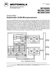
- Page 13 and 14: 1.1 MC68000 The MC68000 is the firs
- Page 15 and 16: SECTION 2 INTRODUCTION The section
- Page 17 and 18: tables. The SFC and DFC registers a
- Page 19 and 20: Register Direct Addressing Data Reg
- Page 21 and 22: BIT DATA 1 BYTE = 8 BITS 7 6 5 4 3
- Page 23 and 24: Notation for operands: PC — Progr
- Page 25 and 26: Table 2-2. Instruction Set Summary
- Page 27 and 28: Table 2-2. Instruction Set Summary
- Page 29: SECTION 3 SIGNAL DESCRIPTION This s
- Page 33 and 34: Table 3-1. Data Strobe Control of D
- Page 35 and 36: 3.6 SYSTEM CONTROL The system contr
- Page 37 and 38: Table 3-3. Function Code Outputs Fu
- Page 39 and 40: SECTION 4 8-BIT BUS OPERATION The f
- Page 41 and 42: A bus cycle consists of eight state
- Page 43 and 44: The descriptions of the eight state
- Page 45 and 46: CLK S0 S1 S2 S3 S4 S5 S6 S7 S8 S9 S
- Page 47 and 48: SECTION 5 16-BIT BUS OPERATION The
- Page 49 and 50: CLK S0 S1 S2 S3 S4 S5 S6 S7 S0 S1 S
- Page 51 and 52: The word and byte write-cycle timin
- Page 53 and 54: STATE 7 On the falling edge of the
- Page 55 and 56: STATE 12 STATE 13 STATE 14 STATE 15
- Page 57 and 58: The breakpoint acknowledge cycle is
- Page 59 and 60: PROCESSOR REQUESTING DEVICE REQUEST
- Page 61 and 62: us request signal. When no acknowle
- Page 63 and 64: RA 1 RA GT 1 XA RA GT RA GT RA XX R
- Page 65 and 66: BUS RELEASED FROM THREE STATE AND P
- Page 67 and 68: BUS THREE-STATED BG ASSERTED BR VAL
- Page 69 and 70: BUS THREE-STATED BG ASSERTED BR VAL
- Page 71 and 72: CLK S0 S2 S4 S6 FC2-FC0 A23-A1 AS U
- Page 73 and 74: CLK S0 S2 S4 S6 S0 S2 S4 S6 FC2-FC0
- Page 75 and 76: A double bus fault occurs during a
- Page 77 and 78: Case No. Control Signal 1 DTACK BER
- Page 79 and 80: ADDR AS R/W UDS/LDS DATA DTACK Figu
- Page 81 and 82:
ADDR 11 AS 20A R/W 22 UDS/LDS 55 26
- Page 83 and 84:
On the rising edge of the clock, at
- Page 85 and 86:
Parameter #47 of Section 10 Electri
- Page 87 and 88:
The privilege mode is a mechanism f
- Page 89 and 90:
6.2 EXCEPTION PROCESSING The proces
- Page 91 and 92:
equests from peripheral devices for
- Page 93 and 94:
6.2.3 Multiple Exceptions These par
- Page 95 and 96:
SSP EVEN BYTE ODD BYTE 7 0 7 0 15 0
- Page 97 and 98:
interrupt priority mask is set at l
- Page 99 and 100:
A signed divide (DIVS) or unsigned
- Page 101 and 102:
After the execution of the instruct
- Page 103 and 104:
. 15 14 13 12 11 10 9 8 7 6 5 4 3 2
- Page 105 and 106:
6.4 RETURN FROM EXCEPTION (MC68010)
- Page 107 and 108:
Table 7-1. Effective Address Calcul
- Page 109 and 110:
In Table 7-5, the following notatio
- Page 111 and 112:
CLR Table 7-7. Single Operand Instr
- Page 113 and 114:
7.9 JMP, JSR, LEA, PEA, AND MOVEM I
- Page 115 and 116:
Table 7-13. Miscellaneous Instructi
- Page 117 and 118:
SECTION 8 16-BIT INSTRUCTION EXECUT
- Page 119 and 120:
Table 8-3. Move Long Instruction Ex
- Page 121 and 122:
Table 8-5. Immediate Instruction Ex
- Page 123 and 124:
8.7 BIT MANIPULATION INSTRUCTION EX
- Page 125 and 126:
Table 8-11. Multiprecision Instruct
- Page 127 and 128:
the handler routine. The total numb
- Page 129 and 130:
9.1 OPERAND EFFECTIVE ADDRESS CALCU
- Page 131 and 132:
Table 9-4. Move Long Instruction Ex
- Page 133 and 134:
9.4 IMMEDIATE INSTRUCTION EXECUTION
- Page 135 and 136:
Table 9-11. Single Operand Instruct
- Page 137 and 138:
Table 9-15. Conditional Instruction
- Page 139 and 140:
Table 9-18. Miscellaneous Instructi
- Page 141 and 142:
SECTION 10 ELECTRICAL AND THERMAL C
- Page 143 and 144:
Table 10-1 summarizes maximum power
- Page 145 and 146:
is lost through the active P-channe
- Page 147 and 148:
10.6 MC68000/68008/68010 DC ELECTRI
- Page 149 and 150:
. 10.9 MC68008 AC ELECTRICAL SPECIF
- Page 151 and 152:
Num Characteristic 8 MHz* 10 MHz* 1
- Page 153 and 154:
S0 S1 S2 S3 S4 S5 S6 S7 CLK 6A FC2-
- Page 155 and 156:
10.11 AC ELECTRICAL SPECIFICATIONS
- Page 157 and 158:
10.12 AC ELECTRICAL SPECIFICATIONS
- Page 159 and 160:
CLK 47 33 BR BG 1 BGACK 35 47 34 37
- Page 161 and 162:
CLK 47 33 BR BG 1 BGACK 35 47 34 37
- Page 163 and 164:
10.13 MC68EC000 DC ELECTRICAL SPECI
- Page 165 and 166:
Num Characteristic 8 MHz 10 MHz 12.
- Page 167 and 168:
S0 S1 S2 S3 S4 S5 S6 S7 CLK 6A FC2-
- Page 169 and 170:
CLK 47 33 BR 34 35 36 BG 39 38 58 A
- Page 171 and 172:
11-2 M68000 8-/16-/32-BIT MICROPROC
- Page 173 and 174:
R/W LDS UDS AS D0 D1 D2 D3 D4 D5 D6
- Page 175 and 176:
A3 1 48 A2 A4 2 47 A1 A5 3 46 A0 A6
- Page 177 and 178:
64 33 L SUFFIX 746-03 B 1 32 A F C
- Page 179 and 180:
64 33 L SUFFIX 746-01 B 1 32 A F C
- Page 181 and 182:
Figure 11-11. Case 765A-05—RC Suf
- Page 183 and 184:
1. Fetch the MOVE instruction. 2. F