X-Band PLL Synthesizer - Radioengineering
X-Band PLL Synthesizer - Radioengineering
X-Band PLL Synthesizer - Radioengineering

Create successful ePaper yourself
Turn your PDF publications into a flip-book with our unique Google optimized e-Paper software.
RADIOENGINEERING, VOL. 15, NO. 1, APRIL 2006 13<br />
X-<strong>Band</strong> <strong>PLL</strong> <strong>Synthesizer</strong><br />
Petr VÁGNER, Petr KUTÍN<br />
Dept. of Radio Electronics, Brno University of Technology, Purkyňova 118, 612 00 Brno, Czech Republic<br />
xvagne02@stud.feec.vutbr.cz, kutin@feec.vutbr.cz<br />
Abstract. This paper deals with design and realization of a<br />
<strong>PLL</strong> synthesizer for the microwave X−band. The synthesizer<br />
is intended for use as a local oscillator in a K−band<br />
downconverter. The design goal was to achieve very low<br />
phase noise and spurious free signal with a sufficient<br />
power level. For that purpose a low phase noise MMIC<br />
VCO was used in phase locked loop. The <strong>PLL</strong> works at half<br />
the output frequency, therefore there is a frequency doubler<br />
at the output of the <strong>PLL</strong>. The output signal from the<br />
frequency doubler is filtered by a band-pass filter and<br />
finally amplified by a single stage amplifier.<br />
Keywords<br />
Microwave <strong>PLL</strong> synthesizer, phase locked loop, low<br />
phase noise, local oscillator, X-band.<br />
1. Introduction<br />
The <strong>PLL</strong> synthesizer is intended for use as a local oscillator<br />
in the K−band downconverter for a satellite receiver.<br />
The local oscillator (LO) signal directly affects the<br />
properties of an intermediate frequency (IF) signal and<br />
consequently the quality of the received information. If the<br />
LO signal had some spurious spectral components, it may<br />
cause conversion of unwanted signals to IF. A phase noise<br />
of the LO causes a distortion of the converted signal, especially<br />
in the case of phase modulation. Therefore, it is<br />
important to achieve a low phase noise, and a spurious free<br />
signal of the local oscillator.<br />
The best results can be obtained with a dielectric<br />
resonator oscillator [1], especially if it is phase-locked [2].<br />
However, components for dielectric resonator oscillator<br />
design are not commonly available. Therefore, we decided<br />
to design a low cost solution using commercially available<br />
integrated circuits.<br />
at 5.976 GHz and its frequency is multiplied by two to<br />
achieve 11.952 GHz. Unfortunately this compromise<br />
brings in phase noise degradation of the output signal by<br />
6 dB compared to the <strong>PLL</strong> signal.<br />
The phase locked loop is designed using monolithic<br />
microwave integrated circuits produced by Hittite Microwave<br />
Corporation. The HMC431 voltage controlled oscillator<br />
running on the frequency of 5.976 GHz is phase<br />
locked to a reference signal at 119.52 MHz. The reference<br />
signal is generated by the 5th overtone quartz oscillator.<br />
This promises a low phase noise close to the carrier. Signals<br />
from the reference oscillator and the feedback loop<br />
come to inputs of the digital phase-frequency detector<br />
(PFD) HMC439. The PFD is intended for use in low noise<br />
<strong>PLL</strong> applications because of its ultra low phase noise floor.<br />
The output signal of the PFD is filtered by the active loop<br />
filter utilizing the fast and low noise operational amplifier<br />
THS4031. The VCO delivers about 2 dBm of output power<br />
to a microstrip directional coupler. The coupled signal is<br />
used as feedback and it is divided by a divider chain with<br />
the total division ratio of 50. This results in the frequency<br />
of 119.52 MHz according to the reference signal. Two<br />
divide-by-5 HMC438 and one divide-by-2 HMC364 low<br />
noise dividers are used.<br />
f REF = 119,52 MHz<br />
quartz oscillator<br />
119,52 MHz<br />
phase frequency<br />
detector<br />
active loop<br />
filter<br />
BW = 1MHz<br />
VCO<br />
5,5 – 6,1 GHz<br />
divide-by-5<br />
freq. divider<br />
divide-by-5<br />
freq. divider<br />
divide-by-2<br />
freq. divider<br />
f 3 = 119,52 MHz<br />
f 2 = 597,6 MHz<br />
f 1 = 2988 MHz<br />
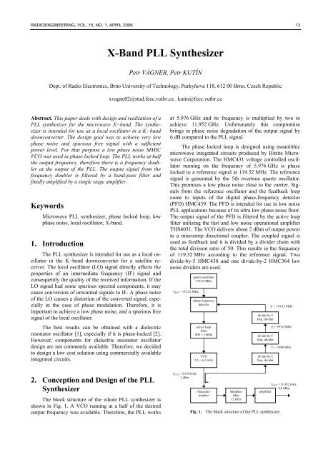
2. Conception and Design of the <strong>PLL</strong><br />
<strong>Synthesizer</strong><br />
The block structure of the whole <strong>PLL</strong> synthesizer is<br />
shown in Fig. 1. A VCO running at a half of the desired<br />
output frequency was available. Therefore, the <strong>PLL</strong> works<br />
f VCO = 5,976 GHz<br />
2 dBm<br />
frequency<br />
doubler<br />
bandpass<br />
filter<br />
12 GHz<br />
f OUT = 11,952 GHz<br />
8,6 dBm<br />
amplifier<br />
Fig. 1. The block structure of the <strong>PLL</strong> synthesizer.
14 P. VÁGNER, P. KUTÍN, X-BAND <strong>PLL</strong> SYNTHESIZER<br />
2.1 The Loop Filter Design<br />
Outside the loop bandwidth, the noise of the free-running<br />
VCO is the dominant noise contributor. The VCO<br />
phase noise is suppressed inside the loop bandwidth. According<br />
to [3] the loop filter bandwidth was designed to be<br />
1 MHz (see Fig. 2). This should ensure a minimal phase<br />
noise of the <strong>PLL</strong>.<br />
Fig. 2. The choice of the loop bandwidth.<br />
Fig. 3 shows an active loop filter with an op-amp. PD D<br />
OUT and PD U OUT are differential outputs of the phase<br />
detector.<br />
K V = 558·10 6 rad/s/V,<br />
K Φ = 0.318 V/rad .<br />
The damping factor ξ is a measure of stability of the<br />
<strong>PLL</strong> and it influences the settling time of the loop. In the<br />
case of our local oscillator, there is no need of a short settling<br />
time. Therefore the damping factor was chosen to be<br />
ξ=1, to avoid stability problems.<br />
Now, if we know the values of ξ and B 3dB , we can<br />
(from equation (6)) calculate the natural frequency ω n .<br />
Then for known K Φ , K V and N, we calculate K from (3) and<br />
the time constants τ 1 and τ 2 from (1) and (2). If R 1 is chosen<br />
to be 400 Ω, then C and R 2 are left to be calculated from<br />
(4), (5). The resulting values are C =1.5 nF and R 2 =580 Ω.<br />
The steady-state phase error, caused by op-amp input<br />
offsets or other imbalances, results (on the phase detector<br />
output) in error pulses of a large amplitude and a short<br />
duration. This signal can cause nonlinear saturation in the<br />
amplifier, reducing its gain bandwidth. This effect is undesirable<br />
to wide bandwidth <strong>PLL</strong>s. One solution is to prefilter<br />
the error pulses before they reach the active filter by<br />
inserting a RC low-pass filter by splitting R 1 and adding C C<br />
(see Fig.4). The capacitor value C C =390 pF was calculated<br />
from:<br />
4<br />
CC<br />
=<br />
(7)<br />
10 ⋅ω<br />
⋅ R<br />
n<br />
1<br />
Fig. 3. The active loop filter.<br />
Our system is a second order type II <strong>PLL</strong>. The natural<br />
frequency ω n and damping factor ξ are given by:<br />
K<br />
ωn = ,<br />
τ<br />
2<br />
K<br />
ξ = (1), (2)<br />
2 τ<br />
τ 1<br />
1<br />
K ⋅ KV<br />
with K = φ . (3)<br />
N<br />
K Φ is the phase detector gain and K V is the VCO tuning<br />
sensitivity. Time constants<br />
τ R 1<br />
C and τ C<br />
(4), (5)<br />
1<br />
=<br />
2<br />
= R 2<br />
are based on the active loop filter components. N is the<br />
divide ratio between the VCO and the phase detector. The<br />
loop bandwidth B 3dB is given by:<br />
ω n<br />
2 2<br />
( 2 + 1) 1<br />
2<br />
B<br />
3<br />
= 2ξ<br />
+ 1+<br />
ξ + . (6)<br />
dB<br />
2π<br />
For our application the following values were given:<br />
Fig. 4. The active loop filter with the pre-integrator.<br />
2.2 Directional Coupler, Frequency Doubler,<br />
<strong>Band</strong>-Pass Filter and Amplifier Design<br />
The directional coupler consists of quarter wavelength<br />
microstrip coupled lines. The coupling loss is approximately<br />
12 dB which, ensures an excitation power of<br />
about -10 dBm at the input of the frequency divider. The<br />
unused gate is terminated using a characteristic impedance<br />
and RF ground (Fig. 5).<br />
An active frequency doubler utilizing one MGF1302<br />
GaAs FET was designed to multiply the <strong>PLL</strong> frequency by<br />
2. The frequency doubler simulated conversion gain is<br />
about 0.3 dB. To obtain a clear output spectrum, the<br />
resulting signal is filtered by a band-pass filter. The filter<br />
consists of two coupled half−wave resonators and its<br />
insertion loss is only 0.6 dB at the center frequency of
RADIOENGINEERING, VOL. 15, NO. 1, APRIL 2006 15<br />
11.952 GHz. The filtered signal is amplified by a single<br />
stage amplifier. The amplifier is designed using MGF1303<br />
with a simulated gain of 8.4 dB. The total conversion gain<br />
of the frequency doubler, band-pass filter and amplifier is<br />
7.9 dB. The simulated output power of the <strong>PLL</strong> synthesizer<br />
is almost 10 dBm. More detailed information about the<br />
design can be found in [4].<br />
Fig. 5. Microstrip directional coupler.<br />
Fig. 7 shows a photograph of the <strong>PLL</strong> synthesizer without<br />
the reference quartz oscillator. The reference oscillator is<br />
attached to the synthesizer via the SMA connector. The<br />
<strong>PLL</strong> synthesizer PCB material is the microwave substrate<br />
DiClad 870 with gold metallization.<br />
Fig. 8. The estimated phase noise of the <strong>PLL</strong> synthesizer.<br />
f offset (kHz)<br />
phase noise<br />
(dBc/Hz)<br />
1 -95<br />
10 -105<br />
100 -109<br />
1000 -111<br />
10000 -138<br />
Tab. 1. The estimated phase noise.<br />
Fig. 9 shows the spectrum of the output signal close to the<br />
carrier measured using HP E7404A spectrum analyzer. We<br />
can see that the spectrum is without any spurious<br />
components. Power level of the carrier is 8.6 dBm, which<br />
is only 1.4 dB less than the simulated value.<br />
Fig. 7. The X-band <strong>PLL</strong> synthesizer.<br />
3. Measured Results<br />
Overall phase noise of the <strong>PLL</strong> synthesizer was predicted<br />
in terms of the loop filter bandwidth, phase noise<br />
floor of the frequency dividers and free running VCO<br />
phase noise. The dashed line in Fig. 8 shows the estimated<br />
phase noise of the <strong>PLL</strong> synthesizer. Numerical values are<br />
given in Tab. 1.<br />
The direct spectrum analyzer phase noise measurement<br />
method was available. RF spectrum analyzers measure<br />
spectral density directly, provided that the phase noise of<br />
the source under test is significantly its AM noise. Limitations<br />
of this direct method are phase noise of the spectrum<br />
analyzer LO, dynamic range and resolution [1].<br />
Fig. 9. The measured spectrum of the output signal – SPAN<br />
500 kHz, RBW 100 Hz, 10 dB/div.<br />
Fig. 10 shows the spectrum of the output signal from<br />
1 GHz to 13 GHz. It is obvious that there is only one undesirable<br />
signal at the frequency of 5.976 GHz. It is the fundamental<br />
frequency of the VCO, suppressed by 28 dB<br />
compared to the <strong>PLL</strong> synthesizer’s first harmonic. There<br />
are no more spurious spectral components in wide bandwidth<br />
so we can say that the spectral purity is much better<br />
than in the case of a signal source realized by means of<br />
multiplying a quartz oscillator (see Fig. 11).
16 P. VÁGNER, P. KUTÍN, X-BAND <strong>PLL</strong> SYNTHESIZER<br />
Output frequency 11.952 GHz<br />
Output power 8.6 dBm<br />
Estimated phase noise f offset = 1 kHz -95<br />
dBc/Hz<br />
f offset = 10 kHz -105<br />
Reference signal frequency 119.52 MHz<br />
Supply voltage +12 V<br />
Supply current 510 mA<br />
Tab. 2. X-band <strong>PLL</strong> synthesizer - main characteristics.<br />
Fig. 10. Spectrum of the <strong>PLL</strong> synthesizer from 1 GHz to 13 GHz.<br />
4. Conclusion<br />
In this paper the design and realization of the local<br />
oscillator for the K−band downconverter is presented. The<br />
LO consists of the <strong>PLL</strong> synthesizer and the reference<br />
quartz oscillator. The output frequency of the <strong>PLL</strong><br />
synthesizer is 11.952 GHz with a power level of approx.<br />
8.6 dBm. Phase noise measurement has shown the phase<br />
noise to be lower than -71 dBc/Hz at the offset frequency<br />
of 1 kHz. We estimate that the true value is -95 dBc/Hz at<br />
this offset. The output signal spectrum is clean and there<br />
are no spurious signals close to the first harmonic. The<br />
realized <strong>PLL</strong> synthesizer meets the design requirements<br />
and can be used as a low-phase-noise local oscillator.<br />
Fig. 11. The spectrum of a multiplied quartz oscillator.<br />
Acknowledgements<br />
The project described in the paper was financially<br />
supported by the FRVŠ project No. 2245/2005.<br />
Fig. 12. The typical phase noise of the HP E7404A and the<br />
measured phase noise of the <strong>PLL</strong> synthesizer at 12 GHz.<br />
As we can see in Fig. 12, the measurement is distorted<br />
because of the spectrum analyzer LO phase noise. The<br />
dashed line shows a typical phase noise of the HP E7404A<br />
at a center frequency of 12 GHz [5]. The solid line shows<br />
our phase noise measurement results. At offset frequencies<br />
lower than 40 kHz, we have measured even lower phase<br />
noise than the typical spectrum analyzer LO phase noise.<br />
Therefore we can say that we have measured the most<br />
likely phase noise of the spectrum analyzer LO. Hence we<br />
can assume that the phase noise of the <strong>PLL</strong> synthesizer is<br />
lower than -71 dBc/Hz at an offset frequency of 1 kHz and<br />
lower than -85 dBc/Hz at 10 kHz.<br />
References<br />
[1] ROHDE, U. L. Microwave and Wireless <strong>Synthesizer</strong>s: Theory and<br />
Design. New York: John Wiley & Sons, 1997. 638 p.<br />
[2] GRAVEL, J-F., WIGHT, J. S. On the conception and analysis of a<br />
12-GHz push-push phase-locked DRO. IEEE Transactions on<br />
Microwave Theory and Techniques, vol. 54, no. 1, January 2006.<br />
[3] ROHDE, U. L. <strong>Synthesizer</strong> Design for Microwave Applications.<br />
. Synergy Microwave Corporation<br />
– Technical Articles, 1999. 51 p.<br />
[4] VÁGNER, P. Kmitočtový syntezátor v pásmu X (X-<strong>Band</strong> <strong>PLL</strong><br />
<strong>Synthesizer</strong>). Diploma thesis. Brno: VUT. 2005 (in Czech).<br />
[5] HEWLETT-PACKARD COMPANY HP E7404A Specifications and<br />
Characteristics. Reference Guide. 1999.<br />
About Authors...<br />
Petr VÁGNER (*1981, 2005 M.Sc. in electrical engg.,<br />
Brno Univ. of Technology) is a Ph.D. student at the Dept.<br />
of Radio Electronics, Brno Univ. of Technology. His main<br />
interests include frequency synthesis.<br />
Petr KUTÍN (*1978, 2002 M.Sc. in electrical engineering,<br />
Brno Univ. of Technology) is a Ph.D. student at the Dept.<br />
of Radio Electronics, Brno Univ. of Technology. His<br />
research interests include microwave circuits.